Custom Teflon PCB Manufacturer & PTFE Prototype Services | Shenzhen Hongda Circuit Technology
Custom Teflon PCB Manufacturer: Low‑MOQ, Fast‑Turn Teflon/PTFE PCBs for RF, Microwave & Aerospace Applications — From First Article to Volume Production on the Same Equipment Platform
Procurement managers and hardware engineering leads at ODM/OEM enterprises face a recurring dilemma when sourcing custom Teflon PCB solutions: prototype shops can turn a 2-layer PTFE board in five days but lack the process discipline for IPC Class 3 volume runs, while mass-production houses demand 500-piece minimums before they will even quote Rogers RT/duroid stackups. That gap between PTFE PCB prototype validation and Teflon PCB production scaling is where most programs lose six to eight weeks — and where Shenzhen Hongda Circuit Technology Co., Ltd. (www.pcbkr.com) has built its operational model.
With 360,000 m² annual capacity, a 30,000 m² ISO-certified facility, and a technology portfolio that spans 224 Gbps ultra-high-speed RF circuits down to single-piece PTFE first articles, Hongda runs prototype and volume jobs on identical lamination, imaging, and metrology platforms. The result is a zero-transfer-risk supply chain: the stackup, impedance model, and surface finish qualified on day five are the same ones shipping at 5,000 pieces per month.
Why PTFE (Teflon) PCBs Demand a Specialist Fabricator — Not a Generalist Shop

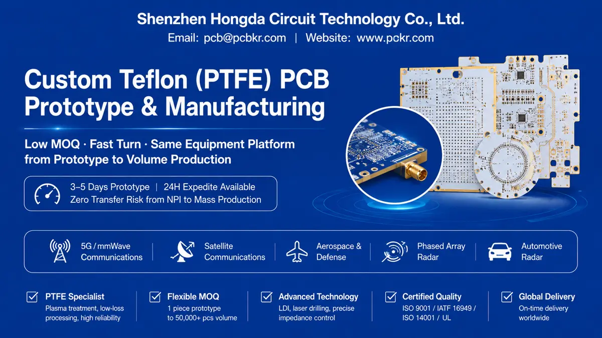
High-Frequency Rogers PTFE PCB with Gold-Plated ENIG Finish Traces
The Material Science Reality Behind Every RF PCB Quote
Polytetrafluoroethylene (PTFE) laminates — marketed under Rogers RT/duroid®, Taconic TLY®, and generic Teflon® brands — behave nothing like standard FR-4. Their dielectric constant (Dk) sits between 2.1 and 2.65, and dissipation factor (Df) can drop below 0.001 at 10 GHz, which is why 5G mmWave, satellite communications, and phased-array radar designs specify them. But those same properties create fabrication challenges that general-purpose PCB houses are not equipped to handle:
- Surface energy mismatch: PTFE is hydrophobic and chemically inert. Without plasma etching or sodium-naphthalene activation prior to lamination, copper peel strength falls below 0.7 N/mm — unacceptable for aerospace thermal cycling.
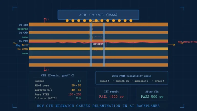
- Coefficient of thermal expansion (CTE): Pure PTFE expands roughly ten times more than copper in the Z-axis. During reflow or thermal vacuum cycling, vias can fracture if the fabricator does not use low-flow bond ply or hybrid ceramic-PTFE stackups.
- Drilling smear: The soft, waxy nature of PTFE produces resin smear in through-holes that standard desmear chemistry cannot remove. Plasma desmear or specialized alkaline permanganate processes are mandatory for reliable through-hole metallization.
At Hongda, these are not afterthought processes. Our vacuum lamination presses are calibrated for PTFE-specific pressure ramps, and every Teflon job receives plasma surface treatment before copper cladding. That is why procurement teams at Intel, NXP, and Continental have qualified our PTFE lines for programs where signal integrity failure is not an option.
Flexible MOQ Structure That Matches Your Procurement Stage

Flexible Teflon PCB Manufacturing: Prototype Validation to Volume Delivery
No-MOQ Prototype Validation for New RF Designs
The most expensive mistake a procurement manager can make is committing to 500 pieces of a PTFE board before the impedance model has been validated with a VNA. Hongda eliminates that risk with a true no-MOQ prototype tier:
| Procurement Stage | Quantity | Typical Use Case | Engineering Deliverables |
|---|---|---|---|
| First Article / NPI | 1 – 5 pcs | Stackup validation, Dk/Df verification, fit-check | DFM report, TDR impedance plot, COC material cert |
| Engineering Pilot | 10 – 50 pcs | Environmental testing, customer qualification | Full electrical test data, S-parameter report (optional) |
| Pre-Production | 100 – 500 pcs | Beta builds, early adopter shipments | Process capability study (Cp/Cpk), FAIR documentation |
| Volume Production | 1,000 – 50,000+ pcs | Mass deployment, long-term supply agreement | PPAP Level 3 (on request), quarterly reliability audits |
This low-MOQ PTFE PCB fabrication model means your R&D team can iterate Rogers 4350B versus RT5880 stackups without burning the procurement budget. One European telecom OEM reduced its NPI spend by 34% in 2025 after switching from a volume-only supplier to Hongda’s flexible tier system.
PTFE Prototype Capability: Speed Without Sacrificing Process Control
Rapid Teflon PCB Prototyping — 3 to 5 Days Standard, 24-Hour Expedite Available
Speed in PTFE prototyping is meaningless if the first article does not electrically match the simulation. Hongda’s prototype line is not a stripped-down quick-turn shop; it is a full-capability pilot line that mirrors our volume floor:
Laser Direct Imaging (LDI) for PTFE Registration Unlike conventional photo-tool exposure, LDI writes each layer directly from Gerber data without film stretching or tooling errors. On PTFE materials — which deform more than FR-4 under lamination pressure — LDI maintains ±25 µm layer-to-layer alignment, critical for multilayer RF boards where via stub length directly impacts return loss at 28 GHz and above.
mSAP (Modified Semi-Additive Process) for Fine-Line RF Structures Millimeter-wave designs often require 30/30 µm trace/space geometries to minimize radiation loss and support compact filter layouts. Hongda’s mSAP line deposits thin copper seed layers followed by resist-defined plating, achieving 30 µm lines with ±3 µm uniformity — impossible with standard subtractive etching on thick copper.
Controlled Impedance Verification via TDR and VNA Every Teflon prototype ships with impedance data. For single-ended RF traces, we guarantee ±5% tolerance (typical ±3%) against your Polar or HyperLynx stackup model. For differential pairs at 112 Gbps PAM4, we provide optional S-parameter extraction to 40 GHz using our in-house vector network analyzer.
Hybrid Stackup Expertise: PTFE + FR-4 + Ceramic Not every design needs a pure PTFE board. Hybrid constructions — e.g., Rogers 4350B core with FR-4 prepreg for non-critical digital layers, or alumina ceramic inserts for thermal management — reduce BOM cost by 20–40% while preserving RF performance. Hongda’s engineering team models these hybrids in Polar Si9000e before cutting a single sheet.
Engineering Support That De-Risks the Procurement Decision
Free DFM Review for Teflon PCB Designs — Response Within 1 Hour
Procurement managers are not RF physicists. They need confidence that the supplier has caught design errors before copper is committed. Hongda’s pre-order engineering review covers:
- Material Selection Guidance: Matching Rogers RT/duroid 5880 (Dk 2.20, lowest loss) versus Taconic TLY-5 (Dk 2.20, cost-optimized) versus Panasonic Megtron 8 (Dk 3.37, high-speed digital hybrid) to your frequency band and budget.
- Stackup Optimization: Recommending copper weight, prepreg thickness, and ground-plane spacing to hit target impedance without over-specifying layer count.
- Manufacturability Flags: Identifying trace-to-pad ratios that will suffer from PTFE etch undercut, or via densities that create lamination void risk.
- Documentation Package: Gerber review notes, stackup drawing, impedance table, and material certificates of conformance (COC) prepared before fabrication starts.
This RF PCB engineering support extends post-delivery. If your test lab reports an impedance deviation, our applications engineers cross-check against the Polar model and lamination records — usually resolving the discrepancy within one business day.
Transparent Lead Time Matrix: Plan Your Build, Not Your Excuses
Teflon PCB Lead Times by Volume and Complexity
| Board Type | Quantity | Standard Lead Time | Expedite Option |
|---|---|---|---|
| 2-layer PTFE prototype | 1–10 pcs | 3–5 days | 24–48 hours |
| 4-layer Rogers prototype | 5–50 pcs | 5–7 days | 48–72 hours |
| 6–8 layer hybrid RF/digital | 50–200 pcs | 7–10 days | 5–7 days |
| 10+ layer high-frequency | 200–1,000 pcs | 10–15 days | 7–10 days |
| Volume production (any layer count) | 1,000+ pcs | 15–25 days | 10–15 days |
What drives the delta? PTFE lamination requires slower heat ramps (1.5–2.0°C/minute versus 3–4°C/minute for FR-4) to prevent resin degradation. Drill feeds must be reduced by 30–40% to avoid PTFE smear. These are physics constraints, not scheduling failures. Hongda’s AI-driven ERP system sequences PTFE jobs on dedicated lamination presses so they do not queue behind standard FR-4 builds — a common delay at mixed-technology factories.
For aerospace and defense procurement teams running MIL-PRF-55110 programs, we offer fixed-slot production planning: your monthly volume is reserved on the lamination calendar, eliminating the “surprise 3-week push-out” that disrupts master production schedules.
Quality Certificates & Compliance That Pass Third-Party Audits
ISO 9001:2015, IATF 16949, and IPC Class 3 as Baseline — Not Aspirational
When a procurement manager onboards a new custom PTFE PCB supplier, the first gate is always the quality packet. Hongda maintains the following active certifications and testing protocols:
- ISO 9001:2015 — Quality management system covering the full fabrication and assembly lifecycle.
- IATF 16949:2016 — Automotive-grade process discipline; relevant when PTFE boards migrate into EV radar and V2X modules.
- ISO 13485:2016 — Medical device quality; applicable for implantable RF telemetry and MRI coil applications.
- IPC-A-600 / IPC-6012 Class 3 — Acceptability and performance standards for high-reliability electronic products.
- RoHS & REACH — Full material declaration compliance for EU and North American environmental regulations.
- MIL-STD-105e / ANSI/ASQ Z1.4 — AQL sampling for incoming material inspection and in-process audits.
Electrical Verification Beyond Go/No-Go Every Teflon board receives 100% flying probe electrical test (ET) for opens and shorts. For RF-specific validation, we offer:
- TDR impedance profiling on coupon structures
- VNA S-parameter measurement to 40 GHz (optional, quoted separately)
- Thermal shock testing per IPC-TM-650 2.6.7 (-55°C to +125°C, 1,000 cycles) for aerospace qualification builds
All test data is archived with lot traceability. If your end customer demands an AS9102 First Article Inspection Report (FAIR), Hongda’s quality team prepares the full dimensional and electrical documentation package within 72 hours of shipment.
Same Equipment, Same Processes: Seamless Scale-Up from Prototype to Production
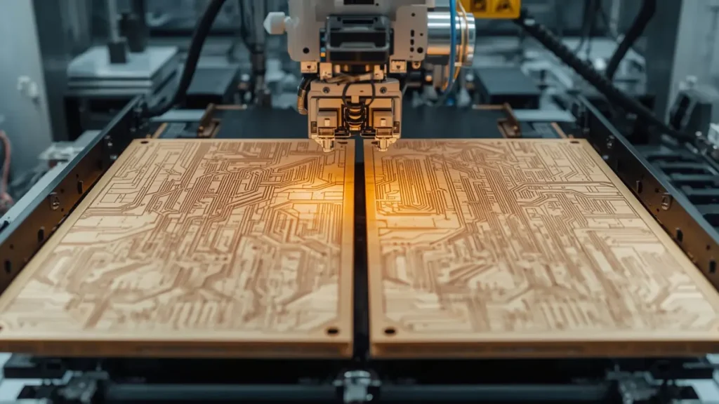
Custom Teflon (PTFE) PCB LDI Exposure & High-Precision Fabrication
The “Prototype-to-Production” Gap Is a Procurement Risk You Can Eliminate
The single biggest source of RF board failure in volume is not design error — it is process drift between the prototype house and the volume supplier. A board that worked at Shop A fails at Shop B because the lamination press curve, plating chemistry, or etch rate differed by 5%.
Hongda solves this structurally. Our prototype line uses the same LDI imagers, vacuum lamination presses, plasma etch systems, and AOI platforms as our volume production floor. When your design moves from 10 pieces to 10,000 pieces, the only variable that changes is the panel count in the loader. That continuity is why our on-time delivery rate exceeds 95% and our customer retention across PTFE programs is above 90% year-over-year.
Ready to Validate Your PTFE Stackup? Get a Quote in 24 Hours
Send PCB Files for Quote — Response Within 24 Hours
Email your Gerbers, stackup requirements, and material preference to Sales@pcbkr.com. Our engineering team will return a firm quote with:
- Material recommendation and Dk/Df validation
- Stackup drawing with impedance table
- Lead time and expedite options
- Quality certificate summary for your audit file
Same Equipment for Prototype & Mass Production — Seamless Scale-Up, Zero Re-Qualification Risk.
Frequently Asked Questions: What Procurement Managers Ask Before Sourcing a Custom Teflon PCB Manufacturer
What is the minimum order quantity (MOQ) for PTFE PCB prototypes, and can I order just one piece for impedance validation?
Hongda supports no-MOQ Teflon PCB prototyping. You can order a single 2-layer Rogers RT5880 board or a 5-piece hybrid stackup for VNA validation. We do not impose volume minimums on first-article builds because we understand that RF designs require electrical proof before procurement can release a production PO. Our prototype pricing is structured to cover true manufacturing cost plus engineering review — there is no artificial markup to compensate for low volume.
How do I verify that a PTFE PCB supplier can actually control impedance within ±5% on Rogers materials, not just quote it?
Ask for three things before placing the order: (a) TDR coupon data from a previous Rogers job with the same Dk, (b) the lamination press temperature profile used for PTFE (should show a ramp rate under 2°C/minute), and (c) whether the supplier uses LDI or film-based imaging (LDI eliminates photo-tool dimensional drift). At Hongda, we provide all three during the quotation phase, and every Teflon prototype ships with measured impedance traces referenced to your Polar model.
What lead time should I realistically expect for a 4-layer Rogers 4350B prototype with ENIG finish?
Standard lead time is 5 to 7 calendar days from Gerber approval to ship. If the design requires mSAP fine-line processing (≤50 µm traces) or hybrid ceramic layers, add 1–2 days for process engineering setup. Expedite service compresses this to 48–72 hours by running the job on a dedicated quick-turn lamination cycle. Note that PTFE cannot be rushed through the same thermal profile as FR-4; “24-hour Teflon” quotes from generalist shops usually indicate they are skipping plasma surface treatment — a failure mode waiting to happen.
Can a China-based PTFE PCB manufacturer support AS9100D or automotive IATF 16949 requirements for aerospace and EV radar programs?
Yes — provided the facility holds the certifications and understands the documentation burden. Hongda is IATF 16949:2016 certified and operates under IPC Class 3 standards with full lot traceability. For aerospace programs requiring AS9100D, we support third-party audits and can prepare AS9102 FAIR packages. Our raw material supply chain includes authorized Rogers and Taconic distributors, ensuring material certificates meet OEM traceability requirements. We have shipped PTFE boards into Tier-1 automotive radar and satellite payload programs since 2022.
Why does my current supplier’s PTFE prototype work, but the volume production batch shows higher insertion loss at 28 GHz?
This is almost always a process-transfer issue. The prototype shop used one lamination press, one lot of prepreg, and one plating line; the volume supplier used different equipment with different thermal mass and chemistry age. PTFE is unforgiving to these variables. Hongda eliminates the transfer entirely by running prototype and volume on the same vacuum lamination presses, LDI imagers, and plasma etch systems. If your design qualified on our prototype line, the volume boards are built with identical process recipes — the only change is panel quantity.
About Author
David Chen https://www.linkedin.com/in/pcbcoming
David Chen boasts an extensive professional background in PCBA manufacturing, PCBA testing, and PCBA optimization, with specialized expertise in high-precision PCBA fault analysis and rigorous PCBA reliability testing. The author has worked with high-layer-count server PCB fabrication, ultra-low-loss backplane stackups, and thermo-mechanical reliability optimization for AI infrastructure projects involving 112G and 224G PAM4 architectures. Skilled in complex circuit design and cutting-edge advanced PCB manufacturing processes, he delivers solutions that elevate product durability and performance across industrial applications. His technical articles focusing on PCBA manufacturing workflows and testing methodologies are widely cited by industry peers, research institutions, and technical platforms, solidifying his reputation as a recognized technical authority in the global circuit board manufacturing sector.