High-Tg FR4 PCB Manufacturing & Prototype Services (Tg ≥ 170°C)
High-Performance, High-Temperature FR4 Printed Circuit Board Manufacturing Services
What Is High-Tg FR4 PCB and Why Is It Critical for High-Reliability Designs?
Understanding Glass Transition Temperature in PCB Substrates
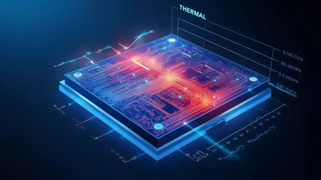
3D thermal endurance model of a High-Tg FR4 PCB (Tg ≥ 170°C) demonstrating heat dissipation stability and dimensional integrity during high-temperature operation.
The glass transition temperature (Tg) marks the point where a polymer substrate shifts from rigid to rubbery state. Standard FR-4 laminates typically exhibit Tg values between 130°C and 140°C. High-Tg FR4 PCB variants are engineered with modified epoxy resins and thermal fillers to achieve Tg ratings of 170°C, 175°C, or even 180°C and above. This elevated threshold fundamentally changes how a board behaves under thermal stress.
In practical terms, when operating temperatures approach or exceed the Tg value, standard laminates undergo rapid Z-axis expansion, increased moisture absorption, and measurable degradation of mechanical strength. High-Tg FR4 materials maintain structural integrity and dimensional stability well beyond the limits of conventional substrates. For procurement teams evaluating high reliability PCB substrate options, this distinction is not merely technical—it directly impacts field failure rates and warranty exposure.
The Lead-Free Soldering Imperative
Global RoHS and REACH mandates have pushed assembly houses toward lead-free reflow profiles with peak temperatures ranging from 250°C to 260°C. Standard FR-4 laminates were never designed to survive repeated excursions into this thermal regime. Delamination, measling, and via barrel fatigue become statistically probable after just a few thermal cycles.
High-Tg FR4 materials, classified under IPC-4101 slash sheets such as /126 and /99, exhibit significantly lower coefficients of thermal expansion (CTE) in the Z-axis—typically below 3.5% between 50°C and 260°C per IPC-TM-650 2.4.24. This reduced expansion minimizes stress on plated through-holes and buried vias during assembly and rework. For buyers sourcing lead-free compatible High Tg PCB solutions, material certification to IPC-4101 is a non-negotiable qualification checkpoint.
When Standard FR-4 Fails: Real-World Failure Modes
Engineers working on multilayer stack-ups with 8 to 20+ copper layers have observed a consistent pattern: boards built on standard Tg material show higher rates of corner cracking, pad lifting, and inner-layer separation after thermal cycling. In automotive under-hood applications where ambient temperatures routinely exceed 125°C, these failures translate to recalls and liability.
The shift to high temperature PCB board substrates is not a luxury specification—it is a risk mitigation strategy. Industries moving toward 800V EV architectures, AI server clusters with sustained thermal loads, and industrial motor drives simply cannot tolerate substrate-level failures.
Key Technical Specifications & Manufacturing Capabilities
Structured Capability Overview
When vetting a High Tg FR4 supplier, procurement professionals should demand transparency across the full manufacturing envelope. The following parameters represent current industry benchmarks for premium fabrication facilities:
| Specification | Capability Range | Relevance to High-Tg Performance |
|---|---|---|
| Board Thickness | 0.2 mm to 6.0 mm | Thicker boards require tighter Z-axis CTE control during lamination |
| Layer Count | 2 to 32+ layers | High layer counts amplify thermal stress; High-Tg resin flow stability is critical |
| Minimum Trace/Space | 3 mil / 3 mil (75 μm) | Fine-line etching demands dimensional stability at elevated press temperatures |
| Copper Weight | 1/3 oz to 6 oz (outer); 1/2 oz to 2 oz (inner) | Heavy copper generates localized heat; High-Tg substrates resist resin softening |
| Surface Finishes | ENIG, ENEPIG, Immersion Silver, Immersion Tin, HASL Lead-Free | Lead-free finishes require compatibility with High-Tg thermal profiles |
| Advanced Features | Blind/Buried Vias, HDI (1+N+1 to Any-Layer), Impedance Control (±5%) | HDI microvias on High-Tg materials demand precise laser drilling and plating chemistry |
HDI and Any-Layer Interconnect on High-Tg Substrates
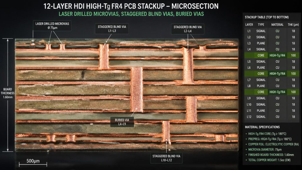
Microscopic Cross-Section Analysis of 12-Layer HDI High-Tg FR4 PCB
The convergence of miniaturization and thermal robustness has driven adoption of High Tg multilayer PCB designs incorporating Any-Layer HDI. At Shenzhen Hongda Circuit Technology, manufacturing lines support laser-drilled microvias down to 75 μm diameter on Tg 170°C and Tg 180°C laminates. The mSAP (modified semi-additive process) enables line width and spacing below 30 μm, critical for 224 Gbps ultra-high-speed signal routing in AI server backplanes.
This capability matters because High-Tg resins historically presented challenges in laser ablation due to altered resin chemistry. Modern formulations from Isola, Shengyi, and ITEQ have resolved these issues, allowing fabricators to combine high thermal endurance with extreme density. For buyers evaluating High-Tg PCB with impedance control and blind vias, the key qualification question is whether the supplier has demonstrated yield stability on HDI stack-ups using certified High-Tg prepregs.
Thermal Stress Testing and Reliability Verification
A reputable ISO certified High Tg PCB factory does not rely on material certificates alone. Thermal stress testing per IPC-TM-650 2.4.25 (DSC method) verifies actual Tg values from production lots, not just raw material datasheets. Supplementary testing includes:
- TMA Z-axis CTE measurement (IPC-TM-650 2.4.24)
- Thermal cycling (-55°C to +125°C, 1000+ cycles per IPC-6012 Class 3)
- Pressure cooker testing (121°C, 100% RH, 96 hours) for moisture resistance
- Solder float test at 288°C for 10 seconds to simulate rework stress
These tests separate suppliers who stock High-Tg materials from those who master High-Tg processing.
Premium High-Tg Materials We Stock
Verified Laminate Grades for Mission-Critical Applications
Material traceability has become a pressing concern in 2026. Lead times for advanced laminates have extended to 140 days in some regions, with high-Tg laminates and low-dielectric-constant materials among the most constrained categories. Shenzhen Hongda Circuit Technology maintains strategic inventory of certified base materials to buffer customers against supply volatility.
| Material Grade | Tg (°C) | Td (°C) | Key Characteristics | Typical Applications |
|---|---|---|---|---|
| Isola 370HR | 180 | 340 | Low CTE, CAF-resistant, lead-free compatible | Telecom base stations, server motherboards |
| Shengyi S1000-2 | 170 | 330 | Cost-optimized High-Tg, high-volume proven | Automotive ECUs, industrial controls |
| ITEQ IT-180A | 180 | 360 | Superior thermal cycling, halogen-free option | EV power inverters, BMS boards |
| Ventec VT-47 | 170 | 325 | Excellent dimensional stability, tight Dk control | 5G mmWave antenna arrays |
| Panasonic Megtron 6 | 185 | 410 | Ultra-low loss, high Tg for high-speed digital | AI accelerator cards, 224Gbps signaling |
Halogen-Free and Sustainability Considerations
Environmental compliance is no longer a regional concern. The EU Ecodesign for Sustainable Products Regulation and similar frameworks in North America and Asia are pushing OEMs to specify halogen-free High Tg FR4 PCB substrates. Halogen-free High-Tg grades achieve flame retardancy through phosphorus and nitrogen chemistry rather than brominated compounds, without sacrificing thermal performance. For procurement teams serving automotive or medical OEMs, halogen-free material certification is increasingly appearing on supplier scorecards.
Why Choose Shenzhen Hongda Circuit Technology for High-Tg PCB Manufacturing?
From Prototype to Mass Production Without Process Translation Errors
Many buyers have experienced the frustration of prototype boards that perform flawlessly, only to encounter yield collapse at volume. This typically stems from prototype shops using different equipment, chemistry, or process parameters than their volume facilities. At pcbkr.com, High-Tg FR4 PCB prototype quote requests are processed on the same lamination presses, drilling platforms, and plating lines used for production volumes.
Our manufacturing ecosystem supports:
- Quick-turn prototypes: 24–72 hour turnaround for 2- to 8-layer High-Tg boards
- Pilot builds: Low-volume validation with full process documentation
- Mass production: Scalable to 10,000+ panels monthly with statistical process control
This continuity eliminates the “second qualification” trap that delays product launches by weeks or months.
Advanced Equipment for High-Tg Precision Fabrication
The mechanical and thermal properties of High-Tg laminates place unique demands on fabrication equipment. Shenzhen Hongda Circuit Technology has invested in platforms specifically optimized for these materials:
- Laser Direct Imaging (LDI): Achieves ±8 μm registration accuracy on High-Tg multilayers, compensating for material shrinkage during hot press cycles
- Vacuum lamination presses with programmable pressure and temperature profiling: Critical for controlling resin flow in High-Tg prepregs, which exhibit different viscosity curves than standard FR-4
- CO₂ / UV laser drilling systems: Optimized pulse parameters for clean microvia formation on Tg 180°C substrates without resin charring
- mSAP plating lines: Enable 30 μm line/space on High-Tg cores for next-generation AI and 5G-Advanced designs
- AI-enhanced AOI and X-ray inspection: Defect detection rates exceeding 99.9%, with particular attention to inner-layer alignment and via barrel integrity on thick High-Tg multilayers
Quality Assurance and Certifications
Procurement decisions in regulated industries require documented evidence of quality system maturity. Our facilities operate under:
- ISO 9001:2015 – Quality management systems
- IATF 16949 – Automotive sector quality requirements
- ISO 14001 – Environmental management
- UL recognition – Flammability and electrical safety
- IPC-A-600 Class 3 and IPC-6012 Class 3 – Performance specifications for high-reliability rigid boards
Every custom High Tg PCB prototype shipment includes a Certificate of Conformance (CoC), material lot traceability, and upon request, cross-sectional micrographs verifying copper thickness, dielectric spacing, and via fill quality.
Applications of High-Tg FR4 PCBs Across Strategic Industries
Automotive Electronics and EV Power Systems
The automotive sector represents the fastest-growing demand vector for automotive grade High Tg FR4. Modern battery electric vehicles incorporate 50 to 150 ECU boards, with BMS (battery management system) and inverter boards operating in ambient temperatures exceeding 130°C. The transition to 800V architectures intensifies thermal management requirements, making Tg 170°C to 180°C laminates standard specification for Tier 1 suppliers.
At Shenzhen Hongda Circuit Technology, automotive High-Tg programs undergo dedicated process flows including ionic contamination testing, thermal shock validation, and full AOI + X-ray coverage. For buyers sourcing High Tg PCB for EV battery management system applications, our IATF 16949 certification and PPAP Level 3 documentation support streamline OEM qualification.
5G-Advanced and Telecommunications Infrastructure
5G-Advanced (Release 18/19) deployment in 2026 is driving demand for High-Tg substrates in massive MIMO antenna arrays, RF front-end modules, and baseband processing cards. Each macro base station requires 8 to 24 PCBs on High-Tg substrates for the active antenna unit alone. These boards must simultaneously manage thermal loads from power amplifiers and maintain signal integrity at mmWave frequencies.
Hybrid laminate systems combining High Tg FR4 with low-loss fillers are increasingly specified for telecom hardware. Our engineering team provides stack-up design support, including mixed-material constructions that position High-Tg cores for thermal management while routing critical RF layers on low-Dk materials.
AI Servers and Data Center Compute
The AI infrastructure buildout has created unprecedented thermal densities in server motherboards and PCIe accelerator cards. A single AI server contains nearly ten times the PCB content value of a conventional server, with backplanes and multilayer compute boards requiring Tg ratings of 170°C to 185°C, controlled-impedance routing at ±5% tolerance, and surface finishes compatible with high-cycle connector mating.
Shenzhen Hongda Circuit Technology manufactures 120+ layer high-density backplanes and 224 Gbps ultra-high-speed RF PCBs for this market, with High-Tg laminates forming the structural backbone of these complex stack-ups.
Industrial Automation and Power Electronics
Variable frequency drives (VFDs), programmable logic controllers (PLCs), and power inverters in industrial settings subject PCBs to continuous thermal cycling, vibration, and exposure to harsh chemicals. High Tg multilayer PCB designs with heavy copper (3 oz to 6 oz) provide the current-carrying capacity and thermal endurance required for Industry 4.0 deployments.
Wide-bandgap semiconductors based on silicon carbide (SiC) and gallium nitride (GaN) operate at junction temperatures exceeding 175°C. Gate driver and power stage boards for these devices must be manufactured on High-Tg substrates to avoid substrate failure under high-temperature switching cycles.
Frequently Asked Questions: A Procurement Buyer’s Guide
What Certifications Should I Verify Before Qualifying a High-Tg PCB Supplier?
Beyond ISO 9001, demand evidence of IATF 16949 (automotive), ISO 13485 (medical), or AS9100 (aerospace) depending on your end market. Critically, verify that the certification scope covers the actual production facility, not just corporate headquarters. Request material certificates verifying Tg compliance via DSC per IPC-TM-650 2.4.25, and ask for thermal cycling test data specific to High-Tg laminates. A supplier unwilling to share defect-rate data in PPM or cross-sectional analysis should be disqualified.
How Do I Evaluate Lead Time and Supply Chain Resilience for High-Tg Materials?
In 2026, lead times for advanced High-Tg laminates have reached up to 140 days. Ask prospective suppliers whether they maintain strategic inventory of certified base materials versus ordering on-demand. At Shenzhen Hongda Circuit Technology, we stock Isola 370HR, Shengyi S1000-2, and ITEQ IT-180A to buffer against supply volatility. For critical programs, negotiate material consignment agreements or dual-source qualification to mitigate single-source risk.
What Is the Real Difference Between Tg 150, Tg 170, and Tg 180 PCB Materials?
Tg 150 materials (often called “Mid-Tg”) offer marginal improvement over standard FR-4 and may survive single-pass lead-free reflow, but they exhibit higher Z-axis expansion and are prone to failure under multiple thermal cycles or rework. Tg 170 and Tg 180 materials provide substantially lower CTE, better chemical resistance, and the mechanical strength required for Class 3 reliability. For automotive, aerospace, or any application with operational temperatures above 130°C, Tg ≥ 170°C is the prudent specification. Tg 180+ becomes necessary for boards with heavy copper, high layer counts, or extended thermal cycling requirements.
Should I Source High-Tg PCBs from a Domestic or China-Based Manufacturer?
This depends on volume, regulatory constraints, and total cost of ownership. China-based manufacturers—particularly in Shenzhen—offer unmatched supply chain integration, faster prototype turnaround, and competitive pricing for mid-to-high volumes. For buyers evaluating High-Tg FR4 PCB manufacturer China options, prioritize facilities with Western-facing quality systems, English-speaking project management, and documented export compliance. The key risk is not geography but supplier maturity: verify audit trails, demand IPC Class 3 workmanship on written POs, and conduct virtual or on-site audits before committing to volume.
What DFM Issues Are Unique to High-Tg PCB Designs?
High-Tg laminates require adjusted process windows during fabrication and assembly. Key DFM considerations include:
1. Pre-bake requirements: High-Tg materials absorb moisture differently; pre-baking per JEDEC J-STD-020E before reflow prevents popcorning
2. Lamination profile: Slower ramp rates and modified pressure curves ensure full cure without voids in thick multilayers
3. Drill parameters: High-Tg resin hardness increases tool wear; optimized feed/speed ratios prevent smearing and resin recession
4. Warpage control: Shadow moiré inspection per IPC-TM-650 2.4.1 should target under 0.75% for Class 3 assemblies
5. Impedance modeling: Stable Dk across temperature on High-Tg substrates enables tighter impedance control, but stack-up design must account for resin content variations
Engage your fabricator early in the design phase—Shenzhen Hongda Circuit Technology provides complimentary DFM reviews for all High-Tg FR4 PCB prototype quote requests to identify these issues before tooling.
Ready to Start Your High-Tg PCB Project?
Whether you are validating a new EV powertrain design, scaling an AI server platform, or qualifying an automotive ECU supplier, substrate selection is a decision with multi-year implications. Shenzhen Hongda Circuit Technology combines certified High-Tg material expertise, advanced HDI and mSAP manufacturing, and rigorous quality systems to de-risk your supply chain.
Upload your Gerber files and stack-up requirements for a free DFM review and competitive quotation. Our engineering team responds to all RFQs within 24 hours.
📧 Email: sales@pcbkr.com
📞 Phone: +86 755 23720053
🌐 Website: www.pcbkr.com
Shenzhen Hongda Circuit Technology Co., Ltd. — Your Strategic Partner for High-Reliability PCB Manufacturing.
About Author
David Chen https://www.linkedin.com/in/pcbcoming
David Chen boasts an extensive professional background in PCBA manufacturing, PCBA testing, and PCBA optimization, with specialized expertise in high-precision PCBA fault analysis and rigorous PCBA reliability testing. The author has worked with high-layer-count server PCB fabrication, ultra-low-loss backplane stackups, and thermo-mechanical reliability optimization for AI infrastructure projects involving 112G and 224G PAM4 architectures. Skilled in complex circuit design and cutting-edge advanced PCB manufacturing processes, he delivers solutions that elevate product durability and performance across industrial applications. His technical articles focusing on PCBA manufacturing workflows and testing methodologies are widely cited by industry peers, research institutions, and technical platforms, solidifying his reputation as a recognized technical authority in the global circuit board manufacturing sector.