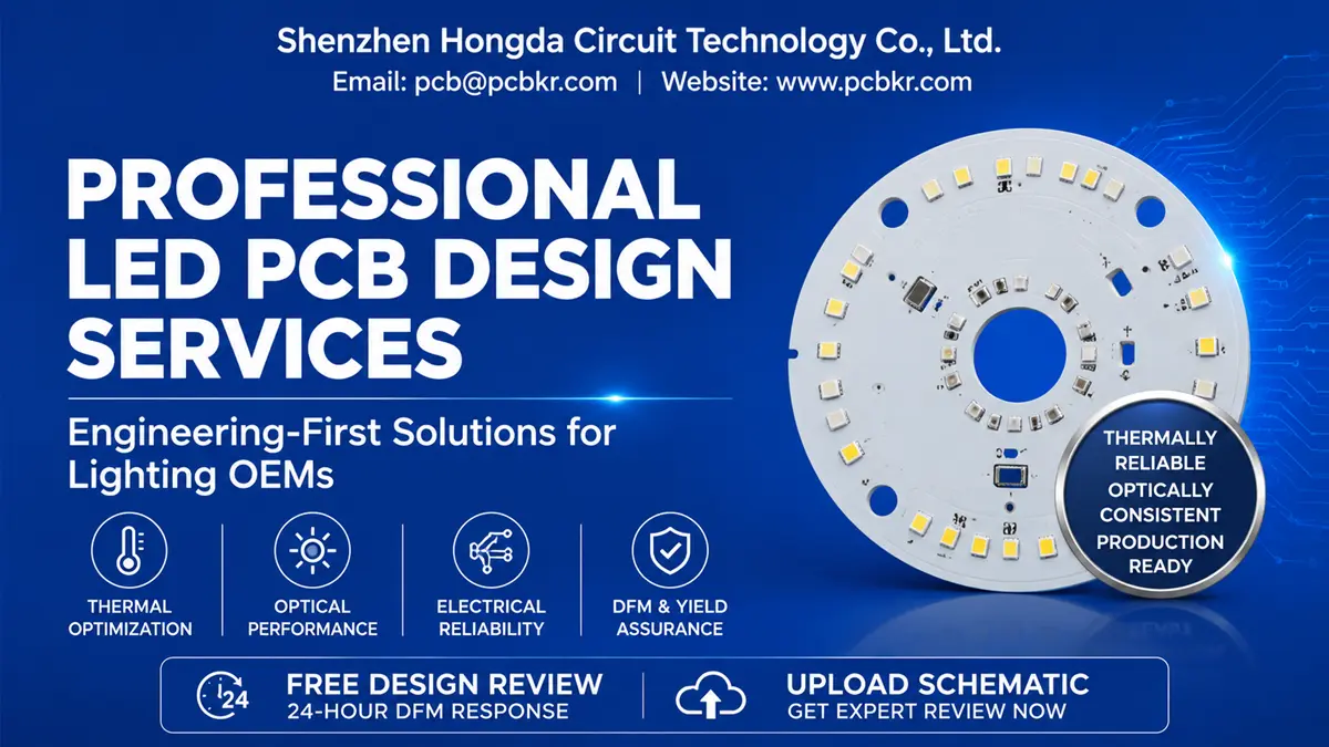
Professional LED PCB Design Services — From Schematic to Production‑Ready Layout
Professional LED PCB Design Services — Engineering‑First Solutions for Lighting OEMs
Every lighting project that fails in the field traces back to one of three root causes: thermal runaway, optical inconsistency, or a manufacturability gap between the designer’s intent and the factory’s capability. At Shenzhen Hongda Circuit Technology Co., Ltd., we have spent eighteen years closing that gap. Our LED PCB design services are not drafting exercises — they are thermal, optical, and electrical engineering workflows that end with a board your SMT line can build at yield, your QC lab can validate, and your customers can install without callbacks.
We support LED PCB board design for commercial lighting, automotive forward‑lighting, horticulture grow systems, high‑density display backplanes, and medical phototherapy equipment. Whether you arrive with a hand‑drawn block diagram or a complete Altium project, our engineering team runs the same gate: can this design survive 10,000 hours of junction‑temperature cycling at target lumen maintenance? If the answer is no, we tell you before you pay for tooling.
Why LED PCB Design Is Different from Standard PCB Layout
A generic PCB layout service treats copper as a connectivity medium. LED PCB design treats copper as a thermal radiator, a current‑distribution network, and an optical substrate simultaneously. The failure modes are different, the materials are different, and the procurement risk is different.
Here is what procurement teams and hardware engineers miss when they treat LED circuit board design as a commodity:
‑ Thermal density. A 100 W COB LED array can concentrate 35 W/cm² at the die attach pad. Standard FR‑4 with 1 oz copper cannot sink that load. The board delaminates, the solder mask browns, and the phosphor degrades. We see this in roughly 40 % of the LED PCB prototyping files that arrive from first‑time customers.
‑ Current‑crowding in parallel strings. When twelve LED strings share a single copper pour, a 5 mV imbalance at the head of the string can shift 30 % of the total current into one branch. That branch dies early. The fixture dims unevenly. The OEM gets a warranty claim twelve months later.
‑ Optical reflectivity. A white solder mask with 78 % reflectance at 550 nm versus 88 % reflectance costs you 11 % of your system lumens. On a 10,000‑lm high‑bay fixture, that is 1,100 lm you are paying for in LED dies but never delivering to the target plane.
‑ Phosphor‑placement tolerance. In chip‑on‑board (COB) LED PCB design, the dam wall around the emitting area must control phosphor overflow to ±0.1 mm. A standard solder‑mask process without optical‑grade registration cannot hold that.
These are not academic concerns. They are the reasons procurement managers at lighting OEMs write supplier corrective‑action requests (SCARs) six months after a product launch. Our LED PCB design services exist to prevent those SCARs at the schematic stage.
The Procurement Engineer’s Guide to Evaluating LED PCB Design Partners
If you are sourcing LED PCB design services for the first time — or replacing a supplier who failed qualification — use this framework. It maps directly to the RFQ questions that separate qualified partners from layout shops.
Thermal Simulation and MCPCB Selection for High Power LED PCB Design
The first question any procurement engineer should ask: does the supplier simulate junction temperature (Tj) before committing to stackup?
At Hongda, we run finite‑element thermal analysis on every high power LED PCB design before layout freeze. We model:
– LED die thermal resistance (Rth j‑s) from the vendor datasheet
– Solder‑layer interface resistance (typical 0.5–2.0 K·cm²/W for SAC305)
– Copper spreading on 1 oz, 2 oz, and 3 oz planes
– Dielectric thermal conductivity (FR‑4 = 0.3 W/m·K; thermally conductive prepreg = 1.5–3.0)
– MCPCB aluminum‑core thickness (1.0 mm, 1.5 mm, 2.0 mm) and interface gap pad
Our 2026 production floor supports metal‑core PCB (MCPCB) fabrication with direct‑bonded copper (DBC) up to 6 oz on 1.5 mm aluminum, as well as ceramic substrates (Al₂O₃ and AlN) for UV‑C and laser‑diode applications where Tj must stay below 85 °C under 15 W/mm² load.
We do not guess at thermal performance. We deliver a thermal report with the Gerber release package, showing ΔTj at nominal drive current, at 110 % overdrive, and at 85 °C ambient. If the numbers exceed the LED vendor’s L70 rating curve, we redesign before you buy a single MCPCB blank.
Optical Design Support and Reflective Solder Mask Specifications
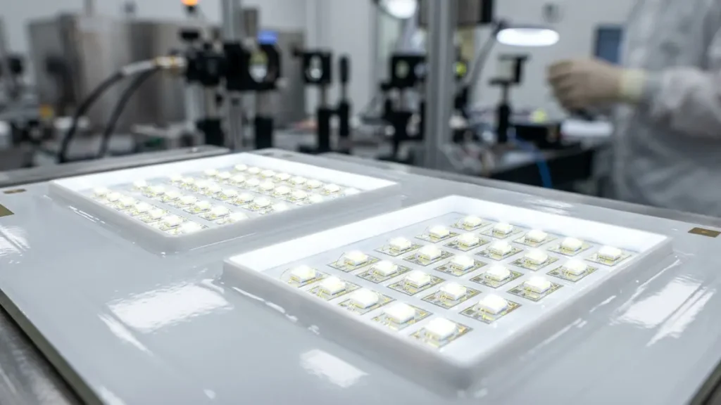
COB LED PCB with High-Reflectivity White Solder Mask & Dam Wall
Lumen uniformity is a procurement issue, not just an engineering issue. A fixture that measures 8,500 lm at center and 6,200 lm at the perimeter fails retail‑channel acceptance criteria in most commercial lighting programs.
Our optical design support team works with your mechanical engineer to:
- Optimize LED pitch‑to‑pitch spacing for the target beam angle and mixing distance.
- Specify solder‑mask reflectivity. We stock Taiyo PSR‑4000 LEW white solder mask rated at ≥88 % reflectance at 550 nm, with a 10‑year UV‑yellowing warranty. For horticulture applications, we can spec high‑reflectivity coatings tuned to the 450 nm / 660 nm pump wavelengths.
- Design COB dam walls with 50 µm positional accuracy, using our LDI (Laser Direct Imaging) exposure system. This prevents phosphor overflow that causes color‑temperature shift (CCT drift) across the emitting surface.
We have shipped LED PCB board design projects with optical uniformity within ±5 % across 600 × 400 mm panels — a specification that requires both layout discipline and manufacturing process control that conventional PCB shops cannot sustain.
LED PCB DFM Analysis That Eliminates Costly Re‑Spins
DFM for LED circuits is not the same as DFM for a router board. The rules are tighter, and the cost of violation is higher.
When you upload your schematic or Gerber package for our free design review, our engineers check against IPC‑2152 current‑carrying tables, but we also apply LED‑specific criteria:
‑ Trace width vs. current density: We flag any 1 oz trace carrying >20 A/cm width, because resistive heating at the copper‑solder‑mask interface accelerates LED degradation.
‑ Thermal via placement: We verify that thermal vias under the LED pad do not break solder‑mask web rules (<0.15 mm remaining web) that cause mask cracking during reflow.
‑ SMT pad geometry: We confirm pad aspect ratios compatible with your pick‑and‑place nozzle library. A 0603 LED pad with 0.3 mm toe extension looks fine on screen but causes tombstoning at 0.15 mm placement tolerance.
‑ Panelization for optical testing: We recommend V‑score or tab‑routing patterns that leave test coupons for luminous‑flux verification without scratching the reflective solder mask.
In 2025, our DFM review process caught thermal‑via starvation in 23 % of inbound LED PCB prototyping files — errors that would have produced boards with 15–25 °C Tj elevation and premature lumen depreciation. We caught them at zero cost to the customer, before phototools were cut.
LED PCB Design with Altium and Proteus Support — No File Format Friction
Your engineering team has already chosen an EDA environment. We do not force migration.
Hongda’s CAM engineering group imports native files from:
– Altium Designer (.PcbDoc, .PrjPcb, .SchDoc)
– Proteus Design Suite (.dsn, .lyt, .brd)
– Cadence OrCAD / Allegro (.brd, .dra)
– Mentor PADS / Xpedition (.pcb, .asc)
– KiCad (.kicad_pcb) — for startup and maker projects
We return a complete manufacturing data package: Gerber RS‑274X, ODB++, IPC‑2581, component centroid (XY) files, and a validated BOM with manufacturer part‑number cross‑references. If you design your own LED PCB in Proteus and need to hand off to a contract manufacturer in Vietnam or Mexico, the data package we generate travels without translation errors.
For customers running embedded firmware alongside hardware, we also support rigid‑flex LED PCB design — a format increasingly common in wearable phototherapy devices and automotive interior lighting modules where the board must fold around mechanical constraints.
Shenzhen Hongda’s 2026 Manufacturing Technology Stack — What Lives on Our Factory Floor
Procurement decisions fail when the RFQ evaluates a supplier’s brochure instead of their production equipment. Here is what actually runs at our 10,000 m² facility in Shenzhen, certified to ISO 9001:2015, IATF 16949:2016, and IPC Class 3.
mSAP and LDI for Ultra‑Fine LED PCB Board Design

Orbotech LDI Exposure System for Fine-Line LED PCB Board Design
In 2026, miniaturized LED modules — especially for micro‑LED display backplanes and AR‑glass light engines — require trace widths below 75 µm. Standard subtractive etching cannot hold the tolerance.
Hongda operates a modified semi‑additive process (mSAP) line that builds copper traces from a 3 µm seed layer, electroplating to final thickness, then flash‑etching the seed. Result: 50 µm line / 50 µm space on production volumes, with impedance tolerance of ±5 % (±3 % on premium tiers). Our Orbotech LDI system images directly onto photoresist without film registration error, eliminating the 5–8 µm misalignment common in contact‑print workflows.
For LED applications, this means:
‑ Finer current‑balancing resistors in multi‑string layouts
‑ Higher routing density under 0.4 mm pitch BGA LED drivers
‑ Reduced board size (and therefore MCPCB aluminum cost) for the same lumen output
AI‑Driven AOI, X‑Ray, and Vacuum Lamination for Zero‑Defect LED PCB Production
A single open microvia under a 100 W LED array becomes a hot spot. A 2 °C local Tj elevation cuts L70 life by 8,000 hours. We do not tolerate that risk.
Our inspection stack:
‑ Koh Young 3D SPI (solder‑paste inspection) + AOI for SMT assembly
‑ Nordson DAGE XD7600NT X‑ray for BGA and microvia void detection
‑ AI‑enhanced AVI (automatic visual inspection) with >99.9 % defect‑capture rate on reflective solder‑mask surfaces
For multilayer LED driver boards (8–16 layers with embedded power planes), we use vacuum lamination presses that hold interlayer registration within ±50 µm across 600 mm panels. Plasma desmear removes resin smear from laser‑drilled microvias down to 75 µm diameter, ensuring barrel plating continuity that survives 20× thermal shock cycling per IPC‑TM‑650 2.6.7.
Back‑Drilling, ENEPIG, and Embedded Component Technology
High‑speed LED driver interfaces — MIPI CSI‑4, USB4, and 10G Ethernet on smart‑lighting gateways — require clean signal paths. Our back‑drilling process trims via stubs to <150 µm with ±50 µm positional accuracy, eliminating the resonant nulls that cause eye‑diagram closure at 56 Gbps.
Surface finish selection matters for LED wire‑bonding and flip‑chip attach:
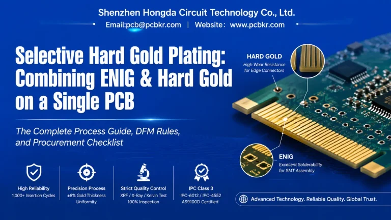
‑ ENEPIG (electroless nickel / electroless palladium / immersion gold): supports gold wire bonding and aluminum wedge bonding without black‑pad risk
‑ OSP for cost‑driven commercial lighting with SMT‑only assembly
‑ Immersion silver for high‑reflectivity pads in chip‑on‑board designs
For 2026, we introduced embedded passive component technology — burying 0201 resistors and capacitors inside Layer 3 of an 8‑layer stackup. On a recent AI‑camera LED ring‑light project, this eliminated 340 surface‑mount passives, reduced PCB real estate by 22 %, and cut parasitic inductance on driver power rails from 800 pH to <200 pH. The result: sub‑1 ns transient response, which means no flicker during PWM dimming.
Our LED PCB Design Services Workflow — Built for Procurement Velocity
We structure the engagement so that procurement managers can gate each phase with clear deliverables and no hidden engineering fees.
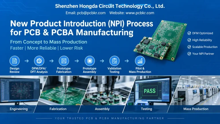
Phase 1: Free Design Review — Upload Schematic for Estimate
Submit your schematic, preliminary layout, or block diagram through our secure portal. Within 24 hours, you receive:
- A DFM checklist (typically 12–25 items) flagged by severity: Critical / Warning / Info
- A stackup recommendation with material Dk/Df values and thermal conductivity
- A preliminary quotation for LED PCB prototyping (8‑day expedite available) and volume production
- A thermal simulation preview if your design exceeds 0.5 W/cm² power density
There is no NDA delay. We sign mutual NDAs within four hours of request.
Phase 2: Co‑Engineering — Thermal, Optical, and Electrical Validation
If you proceed, our engineers lock the stackup and run:
– Full FEA thermal simulation (Ansys Icepak or SolidWorks Flow Simulation)
– Optical ray‑trace validation for COB and lens‑coupled designs
– Signal‑integrity analysis on driver interfaces (if >5 Gbps)
– IPC‑2152 current‑density verification and copper‑weight optimization
You receive a formal engineering review report with redlined layout suggestions, a frozen stackup document, and a manufacturing process flow chart (MPF) for your quality team.
Phase 3: LED PCB Prototyping to Turnkey LED PCB Assembly
Prototype builds run on our standard 15‑day flow, or 8‑day expedite for NPI deadlines. Every proto lot includes:
– First‑article inspection (FAI) report with Cpk data on critical dimensions
– Thermal imaging under operational load
– Lumen‑output and CCT measurement (if optical test fixtures are provided)
– Full ICT or flying‑probe electrical test
For customers who need turnkey LED PCB assembly, our SMT lines handle 01005 passives, 0.23 mm BGA pitch, and mixed‑technology (SMT + through‑hole + wire bond) builds under the same IATF 16949 quality system.
Industry Applications and Compliance Standards We Support
Our LED PCB design services and manufacturing capabilities map to the compliance regimes that procurement teams must verify before supplier onboarding:
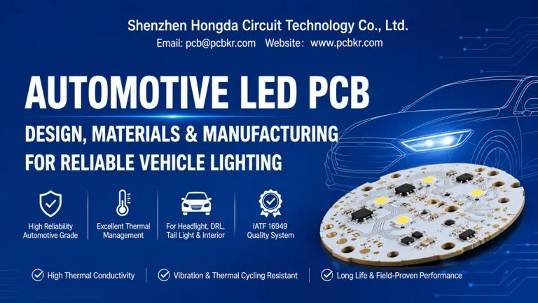
‑ Automotive lighting: AEC‑Q100 / AEC‑Q101 component qualification, PPAP Level 3 submission, IATF 16949:2016 system certification, and ‑40 °C to +125 °C thermal cycling validation.
‑ Commercial / architectural lighting: UL 8750 safety evaluation, LM‑80 / TM‑21 lumen maintenance data integration, and DLC premium qualification support.
‑ Horticulture grow systems: IP65 / IP67 sealing compatibility, 450 nm + 660 nm spectral optimization, and 85 °C / 85 % RH bias testing for greenhouse environments.
‑ Medical phototherapy: IEC 60601‑1 3rd Edition isolation requirements, biocompatibility review for encapsulants, and ISO 13485:2016 medical‑device quality system (available through our partner facility).
‑ Display backplanes: Mini‑LED and micro‑LED pitch requirements (0.4 mm to 1.2 mm), active‑matrix driver integration, and high‑Tg halogen‑free substrates (Tg > 170 °C).
Ready to Design Your Own LED PCB? Start with Engineering Validation, Not Guesswork
The most expensive decision in LED product development is not the LED die cost, the MCPCB blank cost, or the assembly labor. It is the decision to skip thermal and optical validation before committing to tooling.
At Shenzhen Hongda Circuit Technology Co., Ltd., we have built our LED PCB design services around one principle: catch the failure mode at the schematic, not at the 1,000‑hour reliability test. Our 2026 manufacturing technology — mSAP, LDI, AI‑driven AOI, vacuum lamination, and embedded component capability — exists to make that principle scalable from prototype to 2.8 million boards per year.
If you are evaluating LED PCB design manufacturers in Shenzhen, ask the hard questions:
‑ Can you show me a thermal simulation report from a project similar to mine?
‑ What is your actual microvia diameter on production, not on the brochure?
‑ How do you prevent phosphor overflow in COB dam walls at volume?
‑ What is your defect‑escape rate on reflective solder‑mask inspection?
We answer those questions with data, not sales language. Upload your schematic today. We will return a free design review within 24 hours — no purchase order required.
→ Contact: pcb@pcbkr.com
FAQ
How do I verify a LED PCB manufacturer’s thermal design capability before placing an order?
Ask for three documents: (1) a thermal simulation report from a past project with comparable power density, showing FEA mesh and boundary conditions; (2) the stackup drawing with material thermal conductivity values (not just Dk/Df); and (3) a third-party reliability test report (TM-21 or IEC 60749 thermal cycling) for boards built on that stackup. If the supplier cannot produce these, they are guessing. At Hongda, we deliver all three before prototype kickoff.
What is the difference between LED PCB design services and standard PCB layout services?
Standard PCB layout optimizes for signal integrity and routing density. LED PCB design services must simultaneously optimize for thermal spreading, current uniformity across parallel strings, optical reflectivity of the solder mask, and phosphor-dam geometry in COB applications. A standard layout shop will route your LEDs correctly but may place them on 1 oz FR-4 with no thermal vias — a choice that destroys lumen maintenance. Always confirm that the provider runs thermal and optical validation, not just DRC checks.
Which surface finish is best for high-power LED PCB assembly — ENIG, ENEPIG, or OSP?
It depends on your assembly method. For SMT-only commercial lighting with no wire bonding, OSP is cost-optimal and solderable. For COB LED modules with gold wire bonding to the PCB pad, ENEPIG is mandatory — ENIG carries a black-pad risk that causes bond lifts under thermal cycling. For immersion-silver finishes, specify anti-tarnish packaging if storage exceeds 30 days. Hongda offers all three, with ENEPIG at 3 µm Pd / 0.1 µm Au, compatible with 25 µm gold wire bonding.
Can a LED PCB design manufacturer in Shenzhen support automotive lighting PPAP requirements?
Only a subset can. Automotive LED PCB design requires IATF 16949:2016 system certification, AEC-Q100 component qualification support, and PPAP Level 3 documentation (design FMEA, process FMEA, control plan, MSA, and capability studies). Many Shenzhen PCB shops hold ISO 9001 but lack IATF 16949 or automotive program experience. Hongda is dual-certified to ISO 9001:2015 and IATF 16949:2016, with active PPAP submissions for forward-lighting and interior-ambient programs shipping to Tier-1 automotive suppliers.
What file formats should my LED PCB design partner accept — and what should they return?
Accept: native Altium (.PcbDoc), Proteus (.dsn / .lyt), Cadence (.brd), Mentor (.pcb), and Gerber RS-274X. Return: Gerber RS-274X, ODB++, IPC-2581, XY centroid data, and a validated BOM with MPN cross-references. If your partner asks you to “just send PDFs” or “redraw in their format,” that is a capability gap that will introduce errors. Hongda imports native EDA files directly into our CAM system (Ucamco Integr8tor), preserving layer names, net classes, and impedance constraints without manual re-entry.
About Author
David Chen https://www.linkedin.com/in/pcbcoming
David Chen boasts an extensive professional background in PCBA manufacturing, PCBA testing, and PCBA optimization, with specialized expertise in high-precision PCBA fault analysis and rigorous PCBA reliability testing. The author has worked with high-layer-count server PCB fabrication, ultra-low-loss backplane stackups, and thermo-mechanical reliability optimization for AI infrastructure projects involving 112G and 224G PAM4 architectures. Skilled in complex circuit design and cutting-edge advanced PCB manufacturing processes, he delivers solutions that elevate product durability and performance across industrial applications. His technical articles focusing on PCBA manufacturing workflows and testing methodologies are widely cited by industry peers, research institutions, and technical platforms, solidifying his reputation as a recognized technical authority in the global circuit board manufacturing sector.