Ultra-Thin PCB Materials: Thin Substrates & Laminates for High-Frequency and Compact Designs
When procurement teams search for ultra thin PCB material, they are rarely looking for a catalog entry. They are looking for a way to stop field failures, reduce stack-up height, and hit impedance targets on the first spin. At Shenzhen Hongda Circuit Technology Co., Ltd., we have shipped millions of panels using ultra thin PCB materials ranging from standard high-Tg FR-4 cores down to 0.076 mm, through PTFE-based thin PCB substrates for 77 GHz radar, to ceramic-filled thin PCB laminates for AI server backplanes. This guide is written from the shop floor, not a marketing deck. It covers what actually matters when you buy thin PCB substrate and thin PCB laminate in 2026.
What Defines an Ultra-Thin PCB Material? (And Why Standard Spec Sheets Mislead Buyers)
The industry loosely defines ultra thin PCB material as any dielectric system that enables finished board thickness below 0.40 mm. But that definition is incomplete. A 0.20 mm core made from commodity FR-4 with ±10% Dk variation is technically “ultra-thin,” yet it will destroy signal integrity in a 28 GHz 5G antenna module. The real definition must include three attributes:
- Controlled dielectric thickness with tolerances tight enough for impedance modeling (±5% or better at the core level).
- Stable Dk/Df across frequency and temperature, verified by clamped stripline resonator testing per IPC-TM-650 2.5.5.5.
- Compatible copper foil profile — typically HVLP2 or VLP — because conductor loss dominates over dielectric loss once you go below 0.10 mm dielectric thickness at frequencies above 10 GHz.
At PCBKR, we qualify every roll of ultra thin PCB material against these three criteria before it enters our LAUFFER lamination system. We reject approximately 8% of incoming thin-core FR-4 lots due to Dk drift outside our ±0.05 tolerance window. That is the difference between a supplier who stocks material and one who controls it.
Ultra Thin PCB Materials by Dielectric Family — A Procurement-Focused Breakdown
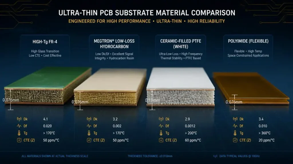
Ultra-Thin PCB Material Comparison: High-Tg FR-4 vs. Megtron, PTFE & Polyimide Substrates
Standard and High-Tg FR-4 Thin Cores (The Workhorse for <10 GHz Designs)
For digital designs operating below 5–10 GHz — IoT gateways, compact industrial controllers, and mid-tier consumer electronics — thin PCB laminate based on high-Tg FR-4 remains the cost-optimized choice. We stock thin cores from 0.076 mm to 0.20 mm with Tg ratings of 150°C, 170°C, and 180°C. The 170°C Tg variant is the sweet spot for lead-free reflow compatibility without the 30–40% cost premium of low-loss hydrocarbon systems.
What to verify on the data sheet:
- Z-axis CTE above Tg (should be <3.5% for 50–260°C to prevent microvia cracking in thin stacks)
- Moisture absorption <0.15% (critical for thin boards that lack the moisture buffer of thicker laminates)
- Copper peel strength >1.05 N/mm after thermal stress
Low-Loss Hydrocarbon and PPE Thin PCB Substrates (The 10–25 GHz Compromise)
When your design crosses into 5G sub-6 GHz, 25G NRZ, or 56G PAM4 territory, standard FR-4 Df (0.015–0.020) becomes a budget killer. Low loss ultra thin PCB material based on hydrocarbon or polyphenylene ether (PPE) resin systems — such as Panasonic Megtron 6 or Isola I-Tera MT40 — delivers Df values of 0.002–0.004 at 10 GHz while maintaining processability close to FR-4.
At PCBKR, we run Megtron 6 thin PCB substrate cores down to 0.10 mm paired with HVLP2 copper foil. The insertion loss improvement versus standard FR-4 with ED copper reaches 1.2–2.8 dB per meter at 28 GHz, depending on trace geometry. For procurement teams, the critical point is this: these materials require lamination pressure profiles 15–20% lower than FR-4 to prevent resin starvation in thin prepreg layers. Our LAUFFER press system maintains ±2 psi accuracy across the panel, which is why we achieve >96% first-pass yield on Megtron 6 builds versus the industry average of 88–91%.
PTFE and Ceramic-Filled PTFE Thin PCB Laminates (The RF/Microwave Standard)
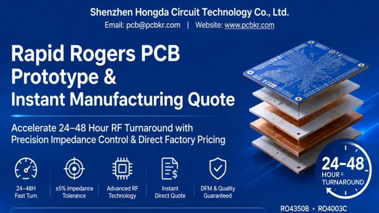
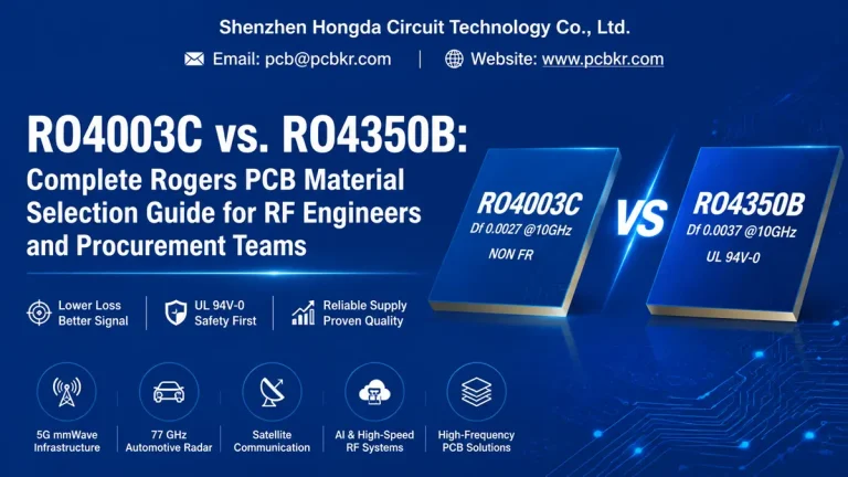
For mmWave radar, satellite payloads, and 6G test fixtures, PTFE thin PCB material remains the reference standard. Pure PTFE (Rogers RT/duroid 5880) offers Dk ≈ 2.20 and Df ≈ 0.0009 at 10 GHz. Ceramic-filled variants (Rogers RO4350B, RO4003C) trade a slight increase in Dk and Df for mechanical stability and a CTE closer to copper, which matters enormously when you are bonding a 0.10 mm thin PCB laminate to an aluminum housing.
Procurement pain point: PTFE does not drill like FR-4. Mechanical drilling below 0.30 mm in PTFE causes fiber tear and smear that desmear chemistry cannot fully clean. Our solution at PCBKR is UV/CO₂ hybrid laser drilling (Mitsubishi systems) with beam profiling optimized for PTFE ablation. We achieve 75 µm microvias in 0.10 mm PTFE cores with <3% void rate, verified by Nordson DAGE 3D X-ray on every qualification lot.
Ceramic Thin PCB Substrates (Al₂O₃, AlN, Si₃N₄) for Power-Dense Hybrid Circuits
When thermal conductivity becomes the dominant constraint — think GaN power amplifiers, EV onboard chargers, or LED driver modules — ceramic filled thin PCB laminate and direct-bond-ceramic (DBC) / direct-plated-ceramic (DPC) substrates enter the conversation. Alumina (Al₂O₃) offers 24–30 W/m·K thermal conductivity with Dk ≈ 9.8. Aluminum nitride (AlN) jumps to 170–230 W/m·K but at 3× the material cost.
At our Shenzhen facility, we operate inline PVD sputtering for DPC ceramic substrates with 20 µm trace precision, plus high-vacuum brazing furnaces for AMB silicon nitride production. For buyers evaluating thin PCB substrate options for power electronics, the decision tree is straightforward: if you need Dk < 4.0 and >100 W/m·K, go AlN or Si₃N₄. If you can tolerate Dk ≈ 9–10 and need cost control, Al₂O₃ DPC is the pragmatic choice.
Flexible and Rigid-Flex Ultra Thin PCB Materials (PI and LCP)
In wearables, medical endoscopes, and foldable consumer devices, flexible ultra thin PCB substrate based on polyimide (PI) or liquid crystal polymer (LCP) provides bend radii down to 3 mm with dielectric thickness starting at 25 µm. LCP offers superior moisture barrier properties (water absorption <0.04%) compared to PI (1.5–3.0%), making it the preferred ultra thin PCB material for implantable medical devices and high-humility automotive sensors.
Thin PCB Substrate vs. Thin PCB Laminate — What Procurement Teams Actually Need to Know
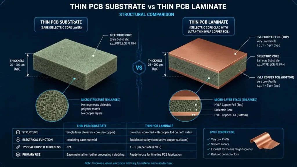
Thin PCB Substrate vs. Thin PCB Laminate: Structural and HVLP Copper Foil Comparison
Buyers frequently conflate these terms. The distinction matters for RFQ accuracy.
| Attribute | Thin PCB Substrate (Core) | Thin PCB Laminate (CCL) |
|---|---|---|
| Definition | Uncopper-clad dielectric sheet | Copper-clad composite (core or prepreg) |
| Typical Thickness Range | 0.025–0.40 mm | 0.076–1.039 mm (copper inclusive) |
| Role in Stackup | Defines interlayer dielectric (ILD) | Provides routing layer + dielectric |
| Critical Spec | Dk uniformity, CTE | Copper peel strength, Dk/Df, Tg |
| Common Pain Point | Batch-to-batch Dk drift | Copper foil profile mismatch with design frequency |
When you issue an RFQ for thin PCB laminate, specify whether you need core material, prepreg, or both. At PCBKR, we see approximately 15% of incoming RFQs from new customers specify “thin laminate” when they actually need thin core + thin prepreg + HVLP copper foil as a bonded set. That ambiguity adds 3–5 days to quotation turnaround and often results in stack-up mismatches. Send your impedance table with the RFQ. We will back-calculate the exact thin PCB substrate and laminate combination.
Key Technical Specifications for Ultra Thin PCB Materials — The Buyer’s Checklist
Electrical Performance: Dk, Df, and Frequency Stability
For high frequency thin PCB substrate selection, Dk and Df are table stakes. The parameter that separates qualified suppliers from catalog merchants is frequency stability. A material rated at Dk 3.40 @ 1 GHz may read 3.28 @ 10 GHz and 3.15 @ 40 GHz. If your SI simulation assumes the 1 GHz number, your 77 GHz radar board will miss impedance by 8–12%.
At PCBKR, we provide measured Dk/Df curves from 1 GHz to 67 GHz using our in-house vector network analyzer (VNA) for every material lot we qualify. We publish these curves in our DFM reports so your modeling team can use frequency-corrected values, not datasheet nominal points.
Thermal Performance: Tg, Td, and Thermal Conductivity
In thin PCB laminate stacks, thermal management is counterintuitive. Thinner dielectrics actually run hotter per unit volume because the heat spreading path is reduced. A 0.10 mm core with 0.3 W/m·K thermal conductivity will show a 15–25°C higher hotspot temperature than a 0.80 mm core under the same current load, all else equal.
Our recommendation: for power-dense ultra thin PCB material applications, specify:
- Tg ≥ 170°C (for lead-free compatibility)
- Td (decomposition temperature) ≥ 340°C
- Thermal conductivity ≥ 0.5 W/m·K if you are running >3 A through traces on thin cores
Mechanical and Dimensional Control
Ultra thin PCB materials warp. It is physics. The CTE mismatch between copper (17 ppm/°C) and FR-4 resin (50–70 ppm/°C above Tg) creates internal stress that manifests as bow and twist after routing. For 0.20 mm finished boards, we target ≤0.5% bow/twist per IPC-6012, but we achieve ≤0.3% on 94% of production lots by using balanced copper fill patterns and controlled cooling profiles in our LAUFFER press.
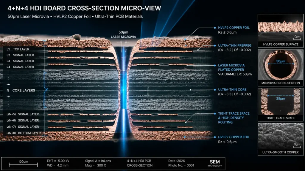
For IC packaging thin PCB material (SLP-class substrates), dimensional stability is even more critical. We maintain ±25 µm layer-to-layer registration on 4+N+4 Any-Layer HDI builds using automated optical registration and dynamic induction riveting — a process spec that aligns with substrate-like PCB (SLP) requirements for mobile SoC packaging.
How to Select Ultra Thin PCB Materials — A Four-Stage Procurement Decision Tree
Stage 1: Frequency and Loss Budget Mapping
- < 5 GHz, loss-tolerant: High-Tg FR-4 thin PCB substrate, 0.10–0.20 mm core, standard ED copper.
- 5–20 GHz, moderate loss budget: Low-loss hydrocarbon thin PCB laminate (Megtron 6, I-Tera MT40) with VLP copper.
- > 20 GHz / mmWave: PTFE or ceramic-filled PTFE ultra thin PCB material with HVLP2 copper and laser-formed microvias.
Stage 2: Thermal and Power Density Screening
- < 2 W dissipation per cm²: Standard thermal design rules apply.
- 2–5 W/cm²: Specify high-Tg thin PCB laminate with thermal vias or transition to metal-core hybrid.
- > 5 W/cm²: Move to AlN ceramic thin PCB substrate or DPC ceramic with active cooling interface.
Stage 3: Dimensional and Assembly Constraints
- BGA pitch ≥ 0.50 mm: Standard thin core + prepreg stackup.
- BGA pitch 0.30–0.40 mm: Any-Layer HDI with ultra thin PCB materials and mSAP process (PCBKR qualifies down to 30/30 µm L/S, with 20/20 µm on the 2026 roadmap).
- Flex-to-install or dynamic flex: PI or LCP flexible ultra thin PCB substrate with rolled-annealed copper.
Stage 4: Supplier Capability and Certification Validation
Do not assume every fabricator can handle ultra thin PCB materials just because they stock thin cores. Verify:
- Material AVL (Approved Vendor List): Do they qualify Megtron, Rogers, Isola, and Taconic, or only generic FR-4?
- Process equipment: LDI exposure (SCREEN Ledia or equivalent) for fine-line imaging; laser drilling for microvias; controlled-pressure lamination for thin stacks.
- Metrology: TDR for impedance, VNA for Dk/Df verification, X-ray for void detection, SEM for copper foil profile characterization.
- Certifications: ISO 9001 is baseline. For automotive, demand IATF 16949. For aerospace, AS9100D. For medical, ISO 13485.
At Shenzhen Hongda Circuit Technology Co., Ltd., we maintain all four certifications under one roof. Our quality system is audited, not self-declared.
Ultra Thin PCB Material vs. Standard Thickness — What Changes at the Manufacturing Level
Ultra-Thin PCB Material Comparison: High-Tg FR-4 vs. Megtron, PTFE & Polyimide Substrates
When you drop from 1.60 mm standard multilayer to 0.40 mm ultra thin PCB laminate, three manufacturing realities shift:
- Registration becomes the primary yield killer. On a 12-layer board with 0.10 mm cores, cumulative layer shift of ±50 µm is catastrophic. We use automated optical registration with sub-micron alignment accuracy and dynamic riveting to hold ±25 µm on 16-layer thin builds.
- Copper roughness dominates insertion loss. On thick boards, dielectric loss is the enemy. On thin boards at high frequency, the copper-to-resin interface becomes the bottleneck. Our switch to HVLP2 foil on Megtron 7 builds improved insertion loss by 1.3 dB/m at 56 GHz versus standard ED copper — a gain equivalent to upgrading the material itself.
- Lamination pressure windows narrow. Too much pressure squeezes resin out of thin prepreg, creating dry spots. Too little pressure leaves voids. Our LAUFFER system uses zone-controlled heating and cooling with 12 independent pressure zones, maintaining ±2 psi across a 24″ × 18″ panel. That is not standard equipment; it is why we can reliably produce 4+N+4 thin PCB substrate stacks that other shops reject as “too exotic.”
B2B Procurement Guide — Evaluating an Ultra Thin PCB Material Supplier
Data Sheet Integrity and Multi-Frequency Characterization
A supplier who quotes thin PCB laminate using only 1 GHz Dk values is selling you a risk. Demand:
- Dk/Df at your operating frequency (or the closest standard test point)
- Temperature coefficient of Dk (TCDk) across your ambient range
- Moisture absorption and its impact on Dk after 85°C/85% RH conditioning
Thin Core and Prepreg Portfolio Depth
Can the supplier source 0.076 mm core? 0.10 mm prepreg with low flow? Ultra-low-profile copper on both sides? At PCBKR, we stock thin cores and prepregs across FR-4, Megtron 6/7/8, Rogers RO4003C/4350B, and RT5880, with thickness increments of 0.025 mm in the critical 0.05–0.20 mm range.
Batch Consistency and Traceability
For ultra thin PCB materials, lot-to-lot Dk variation of ±0.10 can shift impedance by ±3–4 Ω on a 50 Ω line. We enforce incoming material IQC with clamped stripline testing on every lot. Non-conforming material is rejected before it touches a press. Full lot traceability from raw laminate to finished board is standard, not optional.
Supply Chain Resilience for Specialty Materials
Rogers and Panasonic high-frequency thin PCB substrate materials carry lead times of 8–12 weeks in volatile markets. We maintain a 90-day strategic buffer stock of Megtron 6, RO4350B, and RT5880 thin cores to protect customer programs from material allocation shocks. When you issue a 12-month forecast, we align our material hedging to your build plan.
Common Myths About Ultra Thin PCB Materials — What Procurement Teams Get Wrong
Myth 1: “Thinner always means lighter loss.”
Reality: Thinner dielectrics reduce dielectric loss (good), but they also force narrower traces for the same impedance, which increases conductor loss (bad). Below 0.10 mm at 10 GHz, the trade-off often favors slightly thicker material with wider traces and lower-Df resin.
Myth 2: “FR-4 is obsolete for anything above 1 GHz.”
Reality: High-Tg, low-loss FR-4 variants (Dk ≈ 3.7, Df ≈ 0.008) remain viable for 5–8 GHz designs where cost and manufacturability outweigh the last decibel of insertion loss. We have shipped millions of 0.20 mm FR-4 boards for sub-6 GHz 5G small cells that perform flawlessly.
Myth 3: “Dk is the only number that matters.”
Reality: Df, TCDk, moisture absorption, and copper peel strength collectively determine field reliability. A thin PCB laminate with perfect Dk and poor peel strength will delaminate under thermal cycling, turning your “perfect” design into a warranty claim.
FAQ — Ultra Thin PCB Material Procurement from a Buyer’s Perspective
What certifications should I demand when sourcing ultra thin PCB materials from a Chinese manufacturer?
At minimum, verify ISO 9001:2015, IPC-6012 Class 3, and UL 94V-0. For regulated industries, add IATF 16949 (automotive), AS9100D (aerospace), and ISO 13485 (medical). At Shenzhen Hongda Circuit Technology Co., Ltd., we hold all six certifications with full lot traceability and welcome third-party audits. Request our certificate numbers and cross-check them with the issuing bodies — any supplier who hesitates is a red flag.
How do I validate that a supplier’s thin PCB laminate Dk/Df data matches what I will receive in production?
Do not trust datasheet nominal values for thin PCB substrate procurement. Demand a clamped stripline resonator test report (IPC-TM-650 2.5.5.5) on the specific material lot reserved for your build. At PCBKR, we provide measured Dk/Df curves from 1 GHz to 67 GHz for every qualification lot. We also supply impedance coupons with TDR verification on every production panel, so you validate performance on hardware, not paper.
What is the realistic lead time for prototype vs. volume orders using PTFE or Megtron ultra thin PCB materials?
Prototype lead times for PTFE thin PCB material builds are 10–15 business days at PCBKR, assuming material is in stock. Megtron 6/7 thin PCB laminate prototypes run 7–12 days. For volume production, PTFE requires slower drilling feeds and specialized plasma desmear, extending typical volume lead times to 4–5 weeks versus 3–4 weeks for FR-4. We maintain 90-day buffer stock of Rogers and Panasonic materials to buffer allocation risks. Send a 12-month forecast, and we will lock material reservations against your schedule.
Can ultra thin PCB materials support BGA and high-speed signaling (112G/224G PAM4) reliably?
Yes, provided the ultra thin PCB material is paired with the right process technology. At PCBKR, we manufacture 4+N+4 Any-Layer HDI boards using 0.10 mm Megtron 7 cores with 50 µm laser-drilled microvias, achieving insertion loss budgets compatible with 224G PAM4 signaling. The key is not the material alone; it is the combination of low-Df thin PCB substrate, HVLP2 copper, controlled lamination pressure, and sub-micron layer registration. We have shipped 224G-qualified backplanes to AI server OEMs with zero field failures over 18 months in production.
What is the total cost of ownership difference between standard FR-4 thin laminate and low-loss hydrocarbon materials for volume production?
Material cost is only one variable. Low-loss thin PCB laminate (Megtron 6 class) carries a 25–40% material premium over high-Tg FR-4. However, if that material choice allows you to eliminate one relay retimer in a 112G channel, you save $8–15 in BOM cost per board. If it reduces your prototype spin count from three to one, you save 4–6 weeks of NPI time. At PCBKR, we provide total cost of ownership modeling that factors material cost, yield impact, layer count optimization, and signal integrity margin. In approximately 60% of the 112G+ programs we review, the “expensive” material is actually the cheaper program once fully loaded costs are calculated.
Why Shenzhen Hongda Circuit Technology Co., Ltd. for Your Ultra-Thin PCB Material Program
We do not resell material. We engineer with it. Our Baoan, Shenzhen facility integrates:
- SCREEN Ledia LDI Exposure for soldermask and etch resist direct imaging, eliminating phototool degradation that causes pad-size variation in thin-core processing.
- Mitsubishi UV/CO₂ Hybrid Laser Drilling for 50–100 µm microvias in thin PCB substrate stacks up to 4+N+4 configuration.
- LAUFFER Zone-Controlled Lamination with 12 independent pressure zones, critical for preventing resin starvation in 0.076 mm prepreg layers.
- Nordson DAGE 3D X-Ray and In-House VNA to 67 GHz for void detection and Dk/Df lot qualification.
- mSAP Production Line achieving 30/30 µm L/S with a roadmap to 20/20 µm for substrate-like PCB (SLP) applications.
- Full Certification Stack: ISO 9001:2026, IATF 16949, AS9100D, IPC-6012 Class 3/3A, ISO 13485, UL 94V-0.
Whether you are qualifying a thin PCB laminate for a 77 GHz radar module, sourcing ultra thin PCB material for a foldable wearable, or building a 224G PAM4 AI server backplane, our engineering team provides pre-production DFM review, stack-up optimization, and material characterization data before a single panel is cut.
Ready to evaluate your ultra-thin PCB material requirements?
- Email:sales@pcbkr.com
- Engineering:pcb@pcbkr.com
- Address: Room 1608-1610, Research Development Comprehensive Building, Baoyunda Logistics Center, Baoan, Shenzhen, China
About Author
David Chen https://www.linkedin.com/in/pcbcoming
David Chen boasts an extensive professional background in PCBA manufacturing, PCBA testing, and PCBA optimization, with specialized expertise in high-precision PCBA fault analysis and rigorous PCBA reliability testing. The author has worked with high-layer-count server PCB fabrication, ultra-low-loss backplane stackups, and thermo-mechanical reliability optimization for AI infrastructure projects involving 112G and 224G PAM4 architectures. Skilled in complex circuit design and cutting-edge advanced PCB manufacturing processes, he delivers solutions that elevate product durability and performance across industrial applications. His technical articles focusing on PCBA manufacturing workflows and testing methodologies are widely cited by industry peers, research institutions, and technical platforms, solidifying his reputation as a recognized technical authority in the global circuit board manufacturing sector.