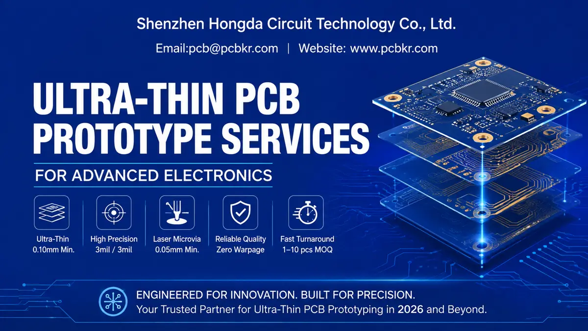
Ultra-Thin PCB Prototype Services for Advanced Electronics
When product teams push the boundaries of miniaturization, the ultra thin PCB prototype becomes the critical gate between concept and commercialization. At Shenzhen Hongda Circuit Technology Co., Ltd., we have observed a clear inflection point in 2026: engineers are no longer asking whether a 0.2 mm board is possible—they are asking whether their thin PCB prototype supplier can deliver it with controlled impedance, zero warpage, and repeatable precision across iterative builds.
This page is not a generic product catalog. It is a technical resource built around the procurement decision chain for buyers sourcing ultra thin PCB prototyping services. We address the specific pain points that delay NPI schedules—material availability, lamination yield, microvia registration, and the gap between prototype capability and mass-production readiness—and explain how Hongda Circuit’s 2026-upgraded equipment stack resolves them.
What Is an Ultra-Thin PCB Prototype?
Technical Definition and Thresholds
An ultra thin PCB prototype is defined as a printed circuit board fabricated for engineering validation with a finished thickness of 0.4 mm or less, commonly ranging from 0.1 mm to 0.3 mm. This category sits distinctly below the industry-standard 1.6 mm FR-4 board and even below the 0.6–0.8 mm “thin PCB” tier. The distinction matters because every 0.1 mm reduction in Z-axis thickness exponentially increases manufacturing risk: dielectric rigidity drops, copper-clad handling becomes critical, and thermal profiles during reflow must be recalibrated.
For procurement teams evaluating prototype thin PCB vendors, the threshold question is not “can you make it thin?” but “can you make it thin and electrically stable?” At Hongda Circuit, our ultra thin PCB prototyping line is configured specifically for this constraint. We support single-sided and double-sided builds down to 0.10 mm finished thickness, with multilayer options up to 4 layers at 0.25–0.40 mm, using ultra-thin FR-4 cores (0.05 mm) and polyimide (PI) substrates (0.025 mm) where flexibility or extreme weight reduction is required.
Why Standard Prototype Shops Struggle With Ultra-Thin Builds
Most commodity PCB prototype houses optimize for speed on 1.0–1.6 mm stackups. When forced into thin PCB prototype territory, they encounter predictable failure modes: core fracture during mechanical drilling, resin starvation in lamination, and plating thickness variation that destroys fine-line impedance. These failures do not surface until the board reaches your lab—wasting days and eroding trust in the supply chain. Hongda Circuit eliminates this risk by isolating ultra-thin work on dedicated production cells with vacuum-assisted material handling and laser-based microvia formation rather than mechanical drill penetration through fragile cores.
Ultra-Thin PCB Prototype Capabilities and Specifications at Hongda Circuit
Thickness Range and Material Stackup
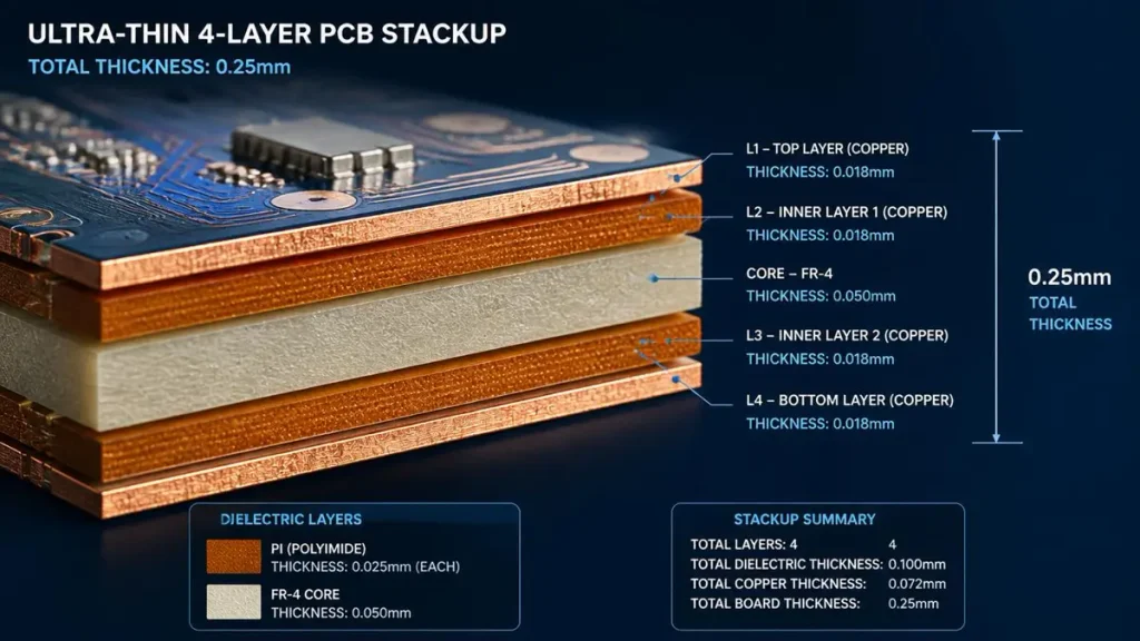
Ultra-Thin 4-Layer PCB Stackup Architecture (0.25mm Total Thickness)
Our ultra thin PCB prototype service covers the following specification envelope:
| Parameter | Capability | Notes for Procurement |
|---|---|---|
| Minimum finished thickness | 0.10 mm (single/double-sided) | Requires PI or ultra-thin FR-4 core |
| Multilayer finished thickness | 0.25–0.40 mm (up to 4 layers) | Sequential lamination with low-pressure cycle |
| Core material options | Ultra-thin FR-4 (0.05 mm core), Polyimide PI (0.025 mm), PET | PI selected for flex-to-install applications |
| Copper weight | 0.5 oz – 2 oz (18–70 µm) | 0.5 oz recommended for ≤0.2 mm builds to reduce etch undercut |
| Minimum trace/space | 3 mil / 3 mil (75 µm / 75 µm) | Achieved via LDI (Laser Direct Imaging) |
| Minimum microvia diameter | 0.05 mm (2 mil) | Laser-drilled; aspect ratio ≤0.75:1 |
| Surface finishes | ENIG, OSP, Immersion Silver | ENIG preferred for ultra-thin boards due to flatness; Immersion Silver for cost-sensitive RF prototypes |
| Maximum panel size | 500 × 500 mm | Thickness-to-area ratio monitored to prevent shipping warpage |
| Prototype MOQ | 1–10 pieces | Optimized for NPI iteration cycles |
Surface Finish Selection for Thin PCB Prototype Reliability
A recurring procurement pain point in ultra thin PCB prototyping is solder joint failure during SMT assembly. Because ultra-thin substrates absorb heat differently than standard boards, HASL (Hot Air Solder Leveling) is generally excluded from our recommendations—the thermal shock and uneven surface topography create coplanarity issues for 01005 and WLCSP components. Instead, we guide buyers toward ENIG (Electroless Nickel Immersion Gold) for its planar surface and oxidation resistance, or Immersion Silver when RF performance demands lower contact resistance. Both finishes are applied in horizontal conveyor lines with reduced thermal exposure to protect the delicate core.
Advanced Manufacturing Technology Powering Our Ultra-Thin PCB Prototyping
The gap between a “capable” prototype and a “production-validated” prototype is determined by the equipment behind it. In 2026, Hongda Circuit completed a targeted upgrade of our ultra-thin production cell. The following technologies directly impact the quality, repeatability, and speed of your thin PCB prototype order.
Laser Direct Imaging (LDI) for Ultra-Fine Line Patterning

Laser Direct Imaging (LDI) Process for Fine-Line Ultra-Thin PCB Fabrication
Traditional film-based photolithography introduces alignment errors and edge roughness that become unacceptable when traces drop below 4 mil. Our LDI systems write the copper pattern directly onto photoresist using a UV laser, eliminating phototools and enabling 3 mil / 3 mil trace-and-space resolution on ultra-thin substrates. For procurement teams, this translates to two tangible benefits: first, the ability to route high-density interconnects on a 0.2 mm board without adding layers; second, faster iteration cycles because design changes require no film remanufacturing—Gerber updates are loaded directly into the LDI workflow.
Dual-Beam Composite Laser Drilling for Microvia Integrity
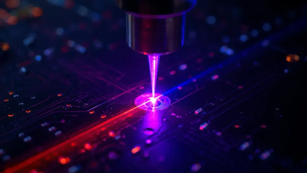
Dual-Beam Laser Microvia Drilling Process (0.05mm Minimum Diameter)
Mechanical drilling through a 0.05 mm FR-4 core is effectively impossible without material tear-out. Our dual-beam laser systems—combining CO₂ lasers for dielectric ablation and UV solid-state lasers for copper breakthrough—produce microvias as small as 0.05 mm (2 mil) with clean sidewalls and minimal heat-affected zone. This matters for prototype thin PCB buyers because microvia quality determines plating uniformity: a laser-drilled hole with a smooth, tapered wall accepts electroless copper more consistently than a mechanically fractured hole, reducing the risk of latent opens during thermal cycling tests.
3D AI X-Ray Inspection for Hidden Defect Detection
Ultra-thin multilayer boards are particularly vulnerable to internal delamination and microvoids in plated through-holes—defects invisible to AOI or electrical test. Our 2026-installed 3D AI X-Ray inspection platform reconstructs the internal layer structure of every ultra thin PCB prototype lot, automatically flagging voids, misregistration, and insufficient copper fill. This step is non-negotiable for medical and aerospace procurement teams who cannot afford field failures on implantable or flight-critical prototypes.
Semi-Additive Process (SAP) for Extreme Density
When your ultra thin PCB prototype design pushes beyond 3 mil traces into substrate-like territory, we deploy Semi-Additive Process (SAP) manufacturing. Unlike subtractive etching—which removes copper and inherently introduces trapezoidal trace profiles—SAP builds copper traces by electroplating through a patterned resist mask, then flash-etching the thin seed layer. The result is near-vertical trace sidewalls with uniform cross-sections, critical for controlled impedance in high-speed wearable and IoT RF modules.
AI-Driven Process Control and Smart Factory Integration
Warpage is the single largest yield killer in thin PCB prototype production. Our lamination presses are integrated with real-time pressure, temperature, and resin-flow sensors governed by AI process-control algorithms. The system adjusts press cycles dynamically based on copper distribution patterns in your Gerber data, preventing the asymmetric stress that causes boards to curl after reflow. For buyers, this means the first article you receive is dimensionally stable enough for direct SMT assembly without carrier fixtures—saving time and tooling cost.
Ultra-Thin PCB Prototyping Process Flow: From Gerber to First Article
Understanding the manufacturing sequence helps procurement teams ask the right questions during supplier audits. Here is how Hongda Circuit processes a typical ultra thin PCB prototyping order:
Step 1: DFM Review and Stackup Engineering
Upon receiving your Gerber files, our engineering team validates copper balance, trace-to-edge clearances, and microvia aspect ratios. For ultra-thin builds, we specifically check whether your copper pour patterns are symmetrically distributed—an imbalance >15% across the board centerline is flagged for redesign to prevent lamination warpage.
Step 2: Ultra-Thin Substrate Preparation and Cleanroom Handling
Cores below 0.1 mm attract particulate contamination that standard shop floors cannot control. Our ultra-thin cell operates under positive-pressure HEPA filtration. Substrates are degaussed and vacuum-laminated with copper foil in a Class 1000 environment.
Step 3: Electroless Copper Deposition (Non-Pressure Bonding)
Rather than conventional press-lamination that can crush delicate cores, we use an electroless copper seed layer followed by electrolytic plating. This builds uniform copper thickness without mechanical stress on the substrate.
Step 4: LDI Patterning and Precision Etching
The LDI system exposes the resist, and the panel enters a horizontal spray-etch line with pH-controlled chemistry. For 0.5 oz copper on ultra-thin cores, etch time is shortened to prevent over-etching that would undermine 3 mil traces.
Step 5: Laser Microvia Drilling and Desmear
Microvias are drilled using the dual-beam laser sequence described above, followed by plasma desmear to remove resin smear from hole walls without aggressive chemical swelling that could delaminate the core.
Step 6: Low-Pressure Sequential Lamination (Multilayer)
For 4-layer prototype thin PCB builds, inner layers are laminated with prepregs selected for low flow to prevent resin squeeze-out that would alter the finished thickness target. Pressure is ramped in three stages rather than applied instantly, and cooling is controlled at ≤2°C/minute to prevent thermal shock warpage.
Step 7: Ultra-Thin Solder Mask Application
Standard solder mask (30–40 µm) would represent 15–30% of the total board thickness on a 0.15 mm build. We apply liquid photoimageable (LPI) solder mask via spray coating at 10–15 µm thickness, cured in a nitrogen atmosphere to prevent oxidation of exposed copper features.
Step 8: Electrical Test, AOI, and 3D X-Ray Validation
Every panel undergoes 100% flying probe electrical test, followed by AOI for surface defect detection. Multilayer prototypes receive 3D X-Ray sampling to validate internal layer registration and via fill quality.
Step 9: Routing, Dimensioning, and Vacuum Packaging
Because ultra-thin boards warp during conventional router tab removal, we use laser routing for profile definition where possible. Finished boards are interleaved with anti-static paper and vacuum-sealed in moisture-barrier bags to prevent humidity absorption during international transit.
Target Applications: Where Prototype Thin PCBs Deliver Competitive Advantage
Wearable Electronics and Health Monitoring Patches
Smartwatches, continuous glucose monitors, and biometric skin patches demand ultra thin PCB prototypes that conform to curved surfaces without cracking traces. Our PI-based 0.1–0.15 mm prototypes enable designers to validate flex-to-install geometries before committing to flexible printed circuit (FPC) tooling.
Medical Implants and Miniaturized Diagnostic Devices
Implantable neurostimulators and capsule endoscopes require biocompatible substrates with minimal foreign-body profile. Hongda Circuit’s thin PCB prototype service supports medical-grade PI and specialized low-outgassing dielectrics, with full traceability documentation for FDA submission packages.
IoT Sensors and Ultra-Compact Industrial Nodes
Space-constrained IoT devices often integrate antenna structures directly onto the PCB. A 0.2 mm prototype thin PCB with Immersion Silver finish provides both the mechanical platform and the RF ground plane in a single layer-reduced stackup, cutting BOM cost and assembly complexity.
Aerospace and Micro-UAV Systems
Weight is a direct proxy for flight time in drone applications. Our 0.15 mm FR-4 prototypes with ENIG finish have been used to validate power distribution networks in sub-250 gram UAV platforms where every gram of PCB substrate mass matters.
Design Considerations for Thin PCB Prototype Success
Copper Balancing to Prevent Warpage
The most common design flaw we correct during DFM review is asymmetric copper distribution. On a 0.2 mm board, a dense copper ground plane on Layer 1 with sparse traces on Layer 2 will guarantee a banana-shaped panel after reflow. We recommend mirroring copper densities across the board centerline or adding thieving patterns in sparse areas.
Component Selection and SMT Assembly Strategy
Ultra-thin boards cannot support heavy through-hole connectors or large QFP packages without mechanical reinforcement. We advise restricting component selection to low-profile SMDs (≤1.0 mm height) and recommend the use of a carrier fixture during SMT reflow to prevent board sag. Hongda Circuit provides carrier design guidelines as part of our pre-production DFM package.
Impedance Control on Reduced Dielectric Thickness
Thinning the dielectric from 1.6 mm to 0.2 mm collapses the separation between signal traces and reference planes, which lowers characteristic impedance for a given trace width. Our engineering team recalculates stackup impedances using Polar SI9000 field solver data and recommends trace width adjustments before fabrication begins—preventing costly respins.
Thermal Management Without Heatsink Real Estate
Ultra-thin boards have minimal Z-axis thermal mass. We recommend embedding thermal vias (0.2 mm pitch) beneath high-dissipation components and, where possible, using 2 oz copper on outer layers to improve lateral heat spreading without adding board thickness.
Why Procurement Teams Choose Hongda Circuit for Ultra-Thin PCB Prototype Services
3–5 Day Quick-Turn Delivery With Logistics Transparency
NPI schedules do not tolerate 15-day prototype lead times. Our ultra thin PCB prototyping cell operates on a dedicated quick-turn queue with 3–5 day standard delivery (including DFM review and electrical test) and 48-hour expedite options for DFM-ready designs. Real-time order tracking is available through our customer portal at pcb@pcbkr.com.
Engineering-First DFM Support, Not Just Order-Taking
We reject the “upload Gerber, receive board” model for complex ultra-thin builds. Every order is assigned a manufacturing engineer who reviews stackup, copper balance, and microvia feasibility before CAM processing begins. This front-loaded consultation prevents the hidden cost of respins.
Prototype-to-Production Continuity
A prototype that cannot scale is a strategic liability. Hongda Circuit maintains identical process parameters between our prototype cell and high-volume production lines. When your thin PCB prototype validates successfully, we can transfer the approved stackup and tooling directly to mass production without re-qualification—protecting your timeline and your IP.
1–10 Piece MOQ With Cost-Transparent Quoting
We do not impose punitive minimums on ultra-thin prototypes. Our online quote engine at pcb@pcbkr.com provides instant pricing for 1–10 piece quantities, with line-item breakdowns of material, LDI, laser drilling, and testing costs. No hidden NRE fees, no surprises.
Quality Certifications and Audit Readiness
Our facility is ISO 9001:2015 certified, with processes aligned to IPC-6012 Class 2 and Class 3 standards. For medical and automotive procurement teams, we provide material certificates of conformance, ionic contamination test reports, and full process traceability documentation.
Frequently Asked Questions by Procurement Teams Sourcing Ultra-Thin PCB Prototype Suppliers
What is the thinnest PCB prototype a manufacturer can reliably produce?
The practical minimum for a reliable ultra thin PCB prototype is 0.10 mm finished thickness for single or double-sided builds, achievable with polyimide (PI) or ultra-thin FR-4 cores. At Hongda Circuit, we validate 0.10 mm prototypes through 100% electrical test and dimensional inspection; below this threshold, handling yield drops significantly and SMT assembly becomes impractical without specialized carrier fixtures.
How much does an ultra-thin PCB prototype cost compared to a standard 1.6 mm board?
In 2026, a thin PCB prototype (0.1–0.4 mm) typically carries a 30–60% premium over a standard 1.6 mm prototype of equivalent layer count. For example, a 2-layer ultra-thin prototype (5–10 pieces) ranges from $40–$150, while a 4-layer build ranges from $80–$300. The premium reflects material handling complexity, laser drilling requirements, and lower panel utilization—not simply the core material cost. Hongda Circuit provides instant quotes at pcb@pcbkr.com with no minimum order penalties.
Can ultra-thin PCB prototypes support controlled impedance and HDI microvias?
Yes. With Laser Direct Imaging (LDI) and dual-beam laser drilling, ultra thin PCB prototyping can achieve controlled impedance (±10% tolerance) and microvias down to 0.05 mm (2 mil). The key constraint is aspect ratio: microvia depth-to-diameter must remain ≤0.75:1 to ensure reliable copper plating. Hongda Circuit’s engineering team validates impedance stackups and microvia feasibility during pre-production DFM review.
What surface finish works best for ultra-thin PCB prototypes during SMT assembly?
ENIG (Electroless Nickel Immersion Gold) is the recommended finish for prototype thin PCB assemblies because it provides a planar, oxidation-resistant surface compatible with fine-pitch components (01005, WLCSP). Immersion Silver is an alternative for RF applications requiring low contact resistance. HASL is generally avoided on ultra-thin boards due to thermal shock risk and surface unevenness.
How do I verify that an ultra-thin PCB prototype supplier can actually manufacture what they quote?
Request three specific proof points: (1) equipment list—verify they operate LDI imaging and laser drilling systems, not just mechanical drills; (2) quality data—ask for Cpk values on trace width and plating thickness from recent ultra-thin production lots; (3) physical samples—order a 1-piece test coupon before committing to a full prototype panel. At Hongda Circuit, we welcome virtual facility tours and provide sample reports from our 3D AI X-Ray inspection systems upon request.
Get Your Ultra-Thin PCB Prototype Quote Today
Shenzhen Hongda Circuit Technology Co., Ltd. has invested specifically in the equipment, cleanroom infrastructure, and engineering expertise required to manufacture ultra thin PCB prototypes that transition seamlessly to volume production. Whether you are validating a wearable sensor, a medical implant, or a next-generation IoT node, our 3–5 day quick-turn service delivers production-representative prototypes without the production-level MOQ.
Submit your Gerber files and stackup requirements at pcb@pcbkr.com for an instant quote and complimentary DFM review.
Shenzhen Hongda Circuit Technology Co., Ltd. — Precision PCB Manufacturing Since 2006. ISO 9001:2015 Certified. IPC-6012 Class 2 / Class 3 Capable.
About Author
David Chen https://www.linkedin.com/in/pcbcoming
David Chen boasts an extensive professional background in PCBA manufacturing, PCBA testing, and PCBA optimization, with specialized expertise in high-precision PCBA fault analysis and rigorous PCBA reliability testing. The author has worked with high-layer-count server PCB fabrication, ultra-low-loss backplane stackups, and thermo-mechanical reliability optimization for AI infrastructure projects involving 112G and 224G PAM4 architectures. Skilled in complex circuit design and cutting-edge advanced PCB manufacturing processes, he delivers solutions that elevate product durability and performance across industrial applications. His technical articles focusing on PCBA manufacturing workflows and testing methodologies are widely cited by industry peers, research institutions, and technical platforms, solidifying his reputation as a recognized technical authority in the global circuit board manufacturing sector.