Embedded Component PCB Testing: Inspection, Reliability and Validation Guide
Embedded component PCB testing requires a layered inspection strategy combining AOI, 2D/3D X‑ray, microsection analysis, dimensional measurement, electrical testing and reliability validation. Because embedded components, microvias, buried connections and internal solder structures are inaccessible after lamination, no single inspection method can adequately validate the finished PCB.
For manufacturers and buyers of embedded component PCBs, the critical issue is not simply whether a supplier has AOI or X‑ray equipment. The real question is whether the supplier’s inspection plan can detect the specific internal defects created by the board’s component‑embedding architecture.
IPC‑6012F explicitly covers rigid multilayer boards containing blind/buried vias, microvias, active/passive embedded circuitry and cavities, while its 2023 revision expanded requirements related to cavities, internal plated layers, microvia reliability, dielectric spacing and microsection evaluation.
Why Is Embedded Component PCB Testing
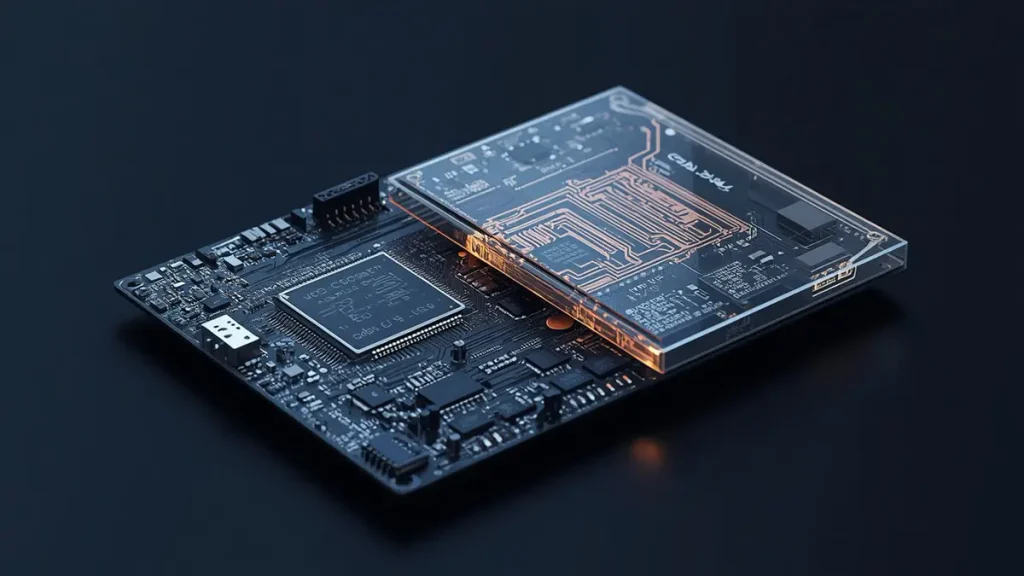
3D Cross-Section of Embedded Component PCB Inspection StructureMore Difficult Than Conventional PCB Inspection?
Direct answer: Embedded component PCB testing is harder because critical components and interconnections are physically buried inside the multilayer structure, making conventional surface inspection incapable of verifying their position, interfaces, solder conditions and internal connectivity.
A conventional PCB can expose most important manufacturing features to AOI, electrical test probes or visual inspection. An embedded‑component PCB changes that relationship.
The finished structure may contain:
‑ Embedded resistors ‑ Embedded capacitors ‑ Embedded ICs or semiconductor devices ‑ Internal solder interfaces ‑ Buried copper connections ‑ Laser microvias ‑ Stacked or staggered microvias ‑ Internal cavities ‑ Copper‑filled vias ‑ Internal dielectric interfaces
The original source correctly identifies visibility as the fundamental challenge and lists embedded components, internal connections, microvias, buried connections, cavities and internal copper structures as typical hidden features.
The manufacturing pain point
The most expensive defects are not necessarily the defects that are easiest to see.
For example, a PCB may pass:
‑ surface AOI, ‑ dimensional inspection, ‑ continuity testing,
yet still contain a latent microvia or internal‑interface defect that becomes electrically unstable after thermal cycling or assembly reflow.
IPC has specifically warned that certain microvia failures can remain latent at room temperature and appear later during reflow, environmental stress screening or field operation.
That changes the inspection philosophy from:
“Does the PCB look good?”
to:
“Can we prove that the internal structure will remain electrically and mechanically reliable throughout its intended thermal and operating environment?”
What Should an Embedded Component PCB Inspection Plan Include?
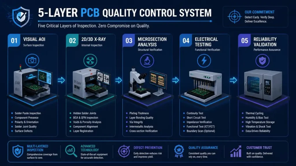
5-Layer Embedded Component PCB Inspection and Quality Control System
Direct answer: A robust inspection plan should normally combine five control layers: visual/AOI inspection, internal X‑ray inspection, structural microsection analysis, electrical verification and application‑specific reliability testing.
A practical manufacturing‑control matrix is:
| Inspection level | Primary purpose | Typical defect detected |
|---|---|---|
| Visual inspection | Surface condition | scratches, contamination, visible defects |
| AOI | Circuit geometry | open/short patterns, pad defects, fine‑line errors |
| 2D/3D X‑ray | Internal visibility | component position, voids, hidden joints |
| Microsection | Physical structure | copper thickness, via interfaces, voids, lamination |
| Electrical test | Connectivity | opens, shorts, isolation failures |
| Reliability testing | Long‑term robustness | latent microvia/interface failures |
| Functional testing | Product behavior | application‑specific electrical failure |
This layered model follows the logic of the original article, which separates testing into visual, internal, structural and electrical validation.
The important engineering principle is defect‑method matching.
An inspection method should be selected according to:
Defect type → physical location → failure mechanism → inspection sensitivity → acceptance criterion
That is much more useful to a procurement engineer than simply listing factory equipment.
What Can AOI Actually Detect on an Embedded Component PCB?
Direct answer: AOI is highly effective for exposed copper patterns, pads, fine‑line structures, solder‑mask features and externally mounted components, but it cannot directly validate most components and connections buried inside the PCB.
AOI can inspect:
‑ Copper trace geometry ‑ Pads ‑ Fine‑line patterns ‑ Solder‑mask registration ‑ Surface contamination ‑ External component placement ‑ Pattern opens ‑ Pattern shorts ‑ Etching‑related defects
The original document identifies AOI as primarily useful for visible PCB features and specifically lists copper patterns, pads, fine lines, surface defects and accessible component placement.
Why AOI becomes insufficient
Imagine a 10‑layer embedded PCB with a passive component positioned between internal dielectric layers.
The component may be:
‑ completely invisible from the top, ‑ inaccessible from the bottom, ‑ surrounded by copper planes, ‑ connected through microvias.
AOI may report the outer copper pattern as acceptable while providing no direct evidence that the internal component is correctly positioned.
Therefore, AOI should be treated as the first inspection layer—not the complete validation system.
How Does X‑Ray Inspection Validate Hidden PCB Structures?
Direct answer: X‑ray inspection provides non‑destructive visibility into buried components, hidden interconnections, internal voids and selected cavity structures that cannot be evaluated directly by optical inspection.
For embedded PCB production, X‑ray can be used to investigate:
‑ Embedded component position ‑ Internal solder structures ‑ Hidden connections ‑ Voids ‑ Cavities ‑ Internal assembly defects ‑ Component orientation ‑ Selected dimensional relationships
The source article specifically identifies these applications for X‑ray inspection.
2D X‑ray versus 3D CT
For procurement decisions, it is useful to distinguish between conventional 2D X‑ray and 3D computed tomography.
2D X‑ray
Useful for:
‑ rapid screening, ‑ solder void evaluation, ‑ component presence, ‑ gross internal positioning, ‑ production‑line inspection.
3D CT
More useful when the engineering question involves:
‑ three‑dimensional component position, ‑ overlapping structures, ‑ complex cavities, ‑ hidden interconnect geometry, ‑ internal spatial relationships.
However, 3D CT is not automatically the correct choice for every production lot. It can introduce higher inspection time, data‑processing requirements and equipment costs.
The correct question is therefore not:
“Does the PCB supplier have CT?”
It is:
“Can the selected X‑ray technology resolve the specific internal structure that represents the product’s dominant failure risk?”
When Should PCB Microsection Analysis Be Used?
Direct answer: Microsection analysis should be used during prototype qualification, process development, failure analysis, reliability investigation and production troubleshooting when physical confirmation of internal PCB construction is required.
A microsection can directly expose:
‑ Copper thickness ‑ Dielectric thickness ‑ Microvia geometry ‑ Plated‑hole structure ‑ Via‑to‑target interfaces ‑ Embedded component placement ‑ Internal voids ‑ Lamination interfaces ‑ Resin distribution ‑ Registration relationships
The original article identifies microsectioning as particularly valuable for prototype qualification, process development, failure analysis, reliability investigation and production troubleshooting.
Engineering pain point: non‑destructive inspection has limits
X‑ray can tell you where something is.
A microsection can often tell you how it was manufactured.
That distinction is critical.
For example, a microvia may appear electrically continuous but still require physical investigation if reliability testing indicates abnormal resistance growth.
IPC’s work on microvia reliability has highlighted weak interfaces between microvia plating and target copper as a potential latent failure mechanism.
Therefore, for high‑reliability embedded PCBs, microsection analysis should not be regarded merely as a cosmetic inspection.
It is a process‑diagnostic tool.
How Should Microvia Reliability Be Validated in an Embedded PCB?
Direct answer: Microvia validation should combine dimensional inspection, cross‑section analysis, electrical continuity and thermal/reliability testing, especially when stacked or complex microvia structures are used.
A modern microvia validation plan can include:
- Via diameter measurement
- Target‑land evaluation
- Copper thickness measurement
- Cross‑section inspection
- Via‑fill evaluation
- Electrical continuity
- Resistance monitoring
- Thermal stress testing
- Reliability coupons
- Failure analysis when abnormal behavior occurs
The source document already identifies cross‑section analysis, electrical continuity, dimensional inspection and reliability testing as relevant microvia evaluation methods.
Why This Matters in Modern PCB Manufacturing
Microvia technology is increasingly integrated with:
‑ HDI build‑up, ‑ fine‑pitch BGA, ‑ stacked microvias, ‑ high‑density routing, ‑ embedded components, ‑ high‑speed signal structures.
IPC‑6012F specifically expanded attention to microvia reliability and introduced test‑coupon approaches better suited to complex interconnected via structures.
IPC technical work has also shown that traditional microsection inspection alone may not identify every latent microvia reliability problem.
This is one reason a mature embedded‑PCB quality system should use both structural inspection and performance‑based testing.
What Electrical Tests Should Be Specified for Embedded Component PCBs?
Direct answer: Electrical verification should normally include continuity and isolation testing, with flying‑probe, fixture‑based or functional testing selected according to production volume, net count, complexity and product requirements.
Typical methods include:
| Test | Main purpose | Best‑fit situation |
|---|---|---|
| Continuity | Detect open circuits | All production levels |
| Isolation | Detect unintended shorts | All production levels |
| Flying probe | Flexible electrical verification | Prototype/low volume |
| Fixture test | Fast repetitive testing | Medium/high volume |
| Functional test | Verify actual product behavior | Finished assembly/product |
| Resistance monitoring | Reliability evaluation | Microvia/interconnect studies |
The original article confirms continuity, isolation, flying‑probe, fixture‑based and functional testing as potential electrical validation methods.
Procurement implication
A supplier should not simply quote:
“100% electrical testing.”
The buyer should ask:
‑ What test coverage is included? ‑ Are embedded component nets included? ‑ What minimum detectable isolation condition is specified? ‑ Is the test based on the Gerber/netlist? ‑ Are special embedded structures excluded? ‑ Is functional testing required? ‑ Are test coupons included for reliability verification?
These questions separate a genuine manufacturing‑control plan from a generic PCB quotation.
How Can PCB Manufacturers Control Embedded Component Position?
Direct answer: Embedded component positioning should be controlled through manufacturing datum strategy, registration measurement, cavity/component dimensional inspection and internal imaging rather than relying solely on surface‑layer registration.
Positioning errors can create several secondary problems.
For example:
Component shift → via misalignment → reduced land overlap → weak interconnection → intermittent electrical behavior
The risk increases when the design combines:
‑ small embedded components, ‑ narrow cavities, ‑ fine‑pitch connections, ‑ laser microvias, ‑ sequential lamination, ‑ thin dielectric layers.
IPC‑7092 specifically addresses design and assembly implementation for embedded components and emphasizes inspection, testing and reliability validation as part of the implementation process.
Practical engineering control
For a new embedded PCB, I would define positional tolerances at three levels:
Component placement → X/Y position and rotation
Cavity → cavity dimensions and registration
Interconnect → pad‑to‑via and via‑to‑target registration
The critical measurement is not necessarily the absolute position of every feature.
It is the remaining process margin between the actual position and the minimum acceptable electrical/mechanical interface.
That is a much more meaningful engineering metric.
What Are the Biggest Manufacturing Pain Points in Embedded Component PCB Production?
Direct answer: The major manufacturing pain points are internal registration, component movement during lamination, thermal stress, microvia reliability, void control, dielectric thickness variation and the difficulty of inspecting structures after they become inaccessible.
Pain Point 1 — Component movement during lamination
Lamination introduces:
‑ heat, ‑ pressure, ‑ resin flow, ‑ dimensional change.
An embedded component that is correctly positioned before lamination may experience positional movement during the subsequent manufacturing sequence.
Pain Point 2 — Internal registration
The supplier must maintain registration across multiple manufacturing stages.
A simplified chain is:
Inner layer → cavity/component → lamination → laser drilling → plating → outer‑layer imaging
An error introduced at one stage can propagate into later interconnections.
Pain Point 3 — Microvia interface reliability
The microvia can pass room‑temperature electrical testing but still possess a latent reliability weakness.
IPC’s published investigations specifically identify microvia interface failures as a significant concern for high‑performance products.
Pain Point 4 — Voids
Voids can occur in:
‑ solder interfaces, ‑ conductive structures, ‑ resin‑rich regions, ‑ embedded attachment areas.
The acceptable level cannot be universally defined without considering the actual structure and application.
Pain Point 5 — Thermal mismatch
During assembly and operation, different materials experience different coefficients of thermal expansion.
The resulting mechanical stress can concentrate around:
‑ vias, ‑ component interfaces, ‑ copper/dielectric boundaries, ‑ solder interfaces.
Pain Point 6 — Inspection after encapsulation
This is the fundamental problem:
The better the component is embedded, the less accessible it becomes for conventional inspection.
That is why inspection must be designed before manufacturing, not added after the board has already been fabricated.
How Should Embedded PCB Testing Be Structured From Prototype to Mass Production?
Direct answer: Testing should become progressively more structured from prototype characterization to process qualification and then production monitoring, with destructive analysis used strategically and non‑destructive inspection used for production control.
Stage 1 — Prototype
Recommended focus:
‑ visual inspection, ‑ AOI, ‑ X‑ray, ‑ microsection, ‑ dimensional measurement, ‑ electrical test.
The objective is process learning.
Stage 2 — Engineering validation
Add:
‑ reliability coupons, ‑ thermal stress evaluation, ‑ microvia evaluation, ‑ component‑position verification, ‑ process capability studies.
The objective is process qualification.
Stage 3 — Pilot production
Establish:
‑ inspection sampling, ‑ control plans, ‑ AOI programs, ‑ X‑ray criteria, ‑ electrical test programs, ‑ microsection frequency, ‑ traceability.
The objective is repeatability.
Stage 4 — Mass production
The emphasis shifts toward:
‑ automated inspection, ‑ statistical process control, ‑ electrical test coverage, ‑ process alarms, ‑ lot traceability, ‑ periodic destructive validation.
The objective is defect escape prevention.
This approach is consistent with IPC’s broader philosophy that inspection criteria should be connected to the intended performance requirements rather than treated as isolated visual checks. IPC‑A‑600 distinguishes externally observable and internally observable conditions, with certain internal conditions requiring microsectioning or other methods for evaluation.
What Today’s PCB Manufacturing Technologies Improve Embedded PCB Validation?
Direct answer: The most relevant modern technologies are high‑resolution AOI, 2D/3D X‑ray, advanced microsectioning, automated dimensional measurement, performance‑based microvia testing, digital manufacturing data and increasingly integrated DFM/DFX workflows.
Several developments are particularly relevant.
1. Advanced HDI manufacturing
Embedded components increasingly coexist with:
‑ blind vias, ‑ buried vias, ‑ microvias, ‑ sequential build‑up, ‑ fine‑line routing, ‑ high‑density BGA structures.
IPC’s current standards framework includes specific design guidance for HDI and embedded circuitry.
2. Performance‑based microvia validation
This is particularly important.
Rather than asking only:
“Does the microsection look acceptable?”
engineers increasingly ask:
“Does the interconnect demonstrate adequate performance under the intended thermal/mechanical stress?”
IPC has published work around reliability testing, via‑chain coupons and thermal‑stress methodologies for detecting latent microvia defects.
3. Digital manufacturing data
IPC‑2581 was developed to improve design‑to‑manufacturing data exchange and includes support for embedded components, cavities, rigid‑flex structures and other advanced PCB technologies.
This creates an important opportunity for modern PCB procurement:
CAD data → DFM → manufacturing → inspection → traceability
The less manual interpretation required between engineering and manufacturing, the lower the risk of undocumented assumptions.
4. More sophisticated X‑ray inspection
For complicated embedded structures, 3D imaging can provide significantly more information than a conventional optical inspection process.
The key is to use advanced inspection technology where the defect physics justify it, rather than adding technology simply for marketing value.
How Should a Procurement Engineer Evaluate an Embedded PCB Supplier?
Direct answer: A procurement engineer should evaluate the supplier by inspection capability, manufacturing process control, reliability evidence, test coverage, traceability and demonstrated experience with the exact embedded structure—not simply by PCB price or equipment list.
A practical supplier audit should include these questions:
| Procurement question | Why it matters |
|---|---|
| Can you inspect embedded components by X‑ray? | Confirms internal visibility |
| Can you provide microsection evidence? | Confirms physical construction |
| How are microvias qualified? | Addresses latent reliability |
| What electrical test coverage is provided? | Controls opens/shorts |
| How is component position verified? | Controls internal registration |
| How are cavities inspected? | Controls dimensional accuracy |
| What reliability coupons are available? | Validates process robustness |
| Can you provide inspection records? | Establishes traceability |
| Which IPC specifications are used? | Defines acceptance framework |
| Can inspection criteria be customized? | Matches product‑specific risk |
For rigid embedded PCBs, IPC‑6012F is particularly relevant because its scope explicitly includes active/passive embedded circuitry and microvia structures.
IPC’s revision table currently lists IPC‑6012 Rev F (September 2023) and IPC‑6017 Rev A (August 2021) for embedded passive devices; it also lists IPC‑7092 Rev A (November 2022) for embedded circuitry implementation. Complete RFQ checklists and the full seven‑stage procurement decision chain are covered in Embedded Component PCB guide.
What Is the Recommended Embedded Component PCB Test Flow?
Direct answer: The recommended flow is AOI → X‑ray → dimensional/structural validation → electrical test → reliability validation, with microsection analysis inserted at prototype, qualification and failure‑analysis stages.
A practical production flow is:
PCB fabrication
↓
Inner‑layer AOI
↓
Component/cavity inspection
↓
Embedded component placement verification
↓
Lamination
↓
X‑ray inspection
↓
Laser drilling
↓
Desmear and metallization
↓
Microvia inspection
↓
Outer‑layer AOI
↓
Electrical continuity/isolation test
↓
Microsection sampling
↓
Reliability validation
↓
Final inspection
↓
FAI / production release
This layered approach directly extends the four‑level inspection structure in the original article while adding process‑specific controls for modern embedded‑component manufacturing.
What Manufacturing Data Should Be Included in an Embedded PCB Quality Report?
Direct answer: A useful quality package should connect the customer’s PCB design requirements to measurable manufacturing and inspection results rather than providing only a generic certificate of conformity.
For a high‑density embedded PCB, a quality package may include:
Dimensional data
‑ Finished board thickness ‑ Layer‑to‑layer registration ‑ Cavity dimensions ‑ Component position ‑ Microvia diameter ‑ Copper thickness ‑ Dielectric thickness
Structural evidence
‑ X‑ray images ‑ Microsection photographs ‑ Via cross‑sections ‑ Lamination interfaces ‑ Embedded‑component interfaces
Electrical evidence
‑ Continuity result ‑ Isolation result ‑ Test coverage ‑ Resistance data where applicable
Process evidence
‑ Material identification ‑ Lot number ‑ Lamination record ‑ Surface‑finish information ‑ Manufacturing date ‑ Inspection records
Reliability evidence
Where specified:
‑ Thermal cycling ‑ Thermal stress ‑ IST or equivalent interconnect evaluation ‑ Reflow simulation ‑ Application‑specific environmental testing
This documentation is especially important when the PCB will be used in automotive, medical, aerospace, industrial control, AI infrastructure or other high‑consequence applications.
What Is the Most Reliable Strategy for Embedded Component PCB Testing?
Direct answer: The most reliable strategy is to match every major physical failure mechanism with at least one appropriate inspection or test method, combining non‑destructive production inspection with selective destructive analysis and reliability testing.
The central engineering principle can be expressed as:
Visibility + Structure + Connectivity + Reliability = Embedded PCB Validation
No single technology provides all four.
AOI provides visibility of external geometry.
X‑ray provides access to hidden structures.
Microsection provides physical evidence of internal construction.
Electrical testing confirms connectivity.
Reliability testing evaluates whether the interconnect survives its intended stress environment.
That is why a modern embedded PCB quality program should not be built around an equipment list.
It should be built around a failure‑mode map.
Embedded Component PCB Testing: Practical Engineering Checklist
Before releasing an embedded‑component PCB to production, confirm:
‑ Embedded component type defined ‑ Component position tolerance defined ‑ Cavity dimensions specified ‑ Internal registration tolerance specified ‑ Microvia structure defined ‑ Via‑fill requirement defined where applicable ‑ AOI coverage established ‑ X‑ray inspection criteria established ‑ Electrical test coverage established ‑ Microsection plan established ‑ Reliability coupon defined ‑ Thermal/reflow requirements identified ‑ IPC performance class identified ‑ Acceptance criteria agreed between customer and supplier ‑ FAI documentation defined ‑ Lot traceability established
FAQs
What should I look for when choosing an embedded component PCB manufacturer?
Choose a manufacturer that can demonstrate embedded-component fabrication, internal X-ray inspection, microsection capability, microvia reliability control, electrical testing and documented process qualification—not simply a low PCB quotation.
Can an embedded component PCB supplier provide X-ray and microsection inspection reports?
A qualified supplier should be able to define when X-ray and microsection inspection are used and provide representative inspection evidence or FAI documentation according to the agreed quality plan.
How does a PCB manufacturer test hidden embedded components?
Hidden components are typically evaluated through X-ray or other internal imaging, while their electrical connections are verified through continuity/isolation testing and, where required, structural analysis and reliability testing.
How can I verify microvia reliability before placing a production order?
Ask the supplier for the applicable microvia design, cross-section evidence, electrical test method and reliability-test/coupon plan. For complex stacked structures, performance-based validation is more informative than relying on visual inspection alone. IPC has specifically documented latent microvia reliability concerns.
Which IPC standards should I specify when purchasing embedded component PCBs?
The applicable standards depend on the PCB construction and end application, but IPC-6012F is a key rigid-board performance specification because its scope includes multilayer boards with microvias and active/passive embedded circuitry; IPC-7092 provides implementation guidance for embedded components.
Conclusion
Embedded component PCB testing is no longer adequately described as a conventional AOI-and-electrical-test operation.
The manufacturing challenge is fundamentally different because the most important structures can disappear inside the PCB during lamination.
A reliable 2026 strategy therefore needs to connect:
Design → DFM → component embedding → lamination → microvia formation → internal inspection → electrical test → reliability validation.
For Shenzhen Hongda Circuit Technology Co., Ltd., this is also the more valuable way to communicate PCB manufacturing capability to international buyers: not by saying that a factory has more machines, but by demonstrating how each inspection technology controls a specific manufacturing risk.
For buyers evaluating an embedded component PCB manufacturer, the strongest supplier is the one that can answer five questions with evidence:
Where can the defect occur?
How will you detect it?
What parameter will you measure?
What is the acceptance criterion?
What evidence will you provide before mass production?
That is the difference between a PCB supplier that simply manufactures boards and an engineering partner that can control embedded-PCB reliability.
Shenzhen Hongda Circuit Technology Co., Ltd.
Email: pcb@pcbkr.com
Website: www.pcbkr.com
About Author
David Chen https://www.linkedin.com/in/pcbcoming
David Chen boasts an extensive professional background in PCBA manufacturing, PCBA testing, and PCBA optimization, with specialized expertise in high-precision PCBA fault analysis and rigorous PCBA reliability testing. The author has worked with high-layer-count server PCB fabrication, ultra-low-loss backplane stackups, and thermo-mechanical reliability optimization for AI infrastructure projects involving 112G and 224G PAM4 architectures. Skilled in complex circuit design and cutting-edge advanced PCB manufacturing processes, he delivers solutions that elevate product durability and performance across industrial applications. His technical articles focusing on PCBA manufacturing workflows and testing methodologies are widely cited by industry peers, research institutions, and technical platforms, solidifying his reputation as a recognized technical authority in the global circuit board manufacturing sector.