High-Density Embedded Component PCB: Engineering and Procurement Guide
A focused cluster page for engineers, OEM buyers, and sourcing teams evaluating embedded component PCB manufacturing—not a general PCB technology overview.
What is the manufacturing definition of a high-density embedded component PCB?
It is a multilayer PCB in which selected passive devices, packaged active devices, or bare dies are formed or placed inside the board and interconnected through controlled dielectric, copper, cavity, microvia, and lamination structures. The manufacturing challenge is not component burial alone; it is maintaining registration, void control, thermal paths, impedance, and inspectability after the internal structure is closed.
IPC-7092A describes embedded-circuitry design, materials, assembly, testing, and reliability considerations; IPC-2316 provides guidance for embedded passive-device boards. These standards are useful process references, but the released drawing and customer qualification plan must define the acceptance criteria.electronics+1
Which embedded components can be manufactured in a high-density PCB?
The practical choices are embedded resistors, capacitors, inductors, passive networks, packaged ICs, and selected bare dies. The right choice depends on component height, termination geometry, thermal dissipation, dielectric compatibility, rework policy, and required electrical access.
| Structure | Typical integration route | Main engineering risk | Best-fit applications |
|---|---|---|---|
| Formed embedded resistor | Resistive foil or printed resistive material in an inner layer | Resistance drift, laser trim access, material uniformity | Termination reduction, precision bias networks |
| Embedded capacitor | High-capacitance laminate or discrete capacitor placed in a cavity | Capacitance tolerance, dielectric loss, lamination voids | Power integrity, RF decoupling, compact modules |
| Embedded inductor | Patterned spiral/meander or discrete component | Q-factor variation, magnetic coupling, heat | RF filtering and power conversion |
| Embedded packaged active | Placed part inside a controlled cavity | Z-height, stress, heat escape, hidden solder joints | Compact controllers and sensor modules |
| Embedded die | Bare die with microvia/RDL or fine interconnect | Die protection, warpage, thermal cycling, yield | Advanced modules, SiP, HPC and sensor integration |
How does the high-density embedded PCB process work?
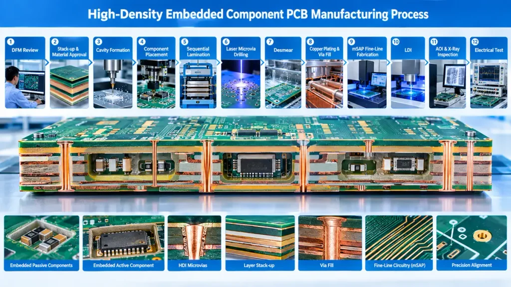
High-Density Embedded Component PCB Manufacturing Process
A controlled process normally runs from DFM and material qualification through inner-layer fabrication, cavity formation or component placement, sequential lamination, laser microvia formation, copper filling/plating, fine-line imaging, inspection, electrical test, and reliability validation.
A production-ready route should be frozen only after the supplier confirms component geometry, cavity datum, adhesive/resin flow, copper balance, laser window, inspection access, and test coupons. A representative flow is:
RFQ package → DFM review → stack-up and material approval → inner-layer imaging/etch or mSAP → cavity machining or formed passive creation → component placement and alignment → lamination → X-ray/ultrasonic or cross-section verification → UV/CO₂ laser drilling → desmear → copper deposition and via fill → outer-layer LDI → AOI → surface finish → electrical test → dimensional inspection → qualification report.
Which numeric design parameters should be locked before quotation?
The RFQ should define component body size and tolerance, Z-height, cavity length/width/depth, cavity-to-copper clearance, layer-to-layer registration, trace/space, via diameter and aspect ratio, copper thickness, dielectric Dk/Df, impedance tolerance, warpage limit, void criterion, and reliability cycles.
| Parameter | Engineering starting point | Release rule |
|---|---|---|
| Fine line/space | 50/50 µm (2/2 mil) is a commercially documented mSAP capability; 8/8 µm should be treated as an advanced, application-specific qualification, not a default PCB rule. | Approve only against a Hongda capability coupon and cross-section. |
| Microvia finished diameter | Typically 60–100 µm for dense HDI concepts | Set laser and pad geometry from the stack-up, not from nominal marketing limits. |
| Microvia aspect ratio | Common design target ≤1:1 for robust laser microvias | Escalate stacked structures and require reliability evidence. |
| Copper thickness | Signal mSAP commonly uses thin seed/base copper; power layers may require 18–70 µm or more | Specify finished copper by layer and allow plating tolerance. |
| Impedance | Define single-ended/differential target, e.g., 50 Ω or 90/100 Ω where applicable | Require coupon measurement and stated tolerance, such as ±10% or customer-defined. |
| Cavity clearance | Use component tolerance + placement tolerance + resin-flow allowance | Do not release a fixed clearance without a lamination DOE. |
| Thermal cycling | Application-specific; -40 to +125 °C and 500–1,000 cycles are common qualification ranges in industry test programs. | Customer specification and applicable IPC method control acceptance. |
Important distinction: a supplier’s smallest laboratory geometry is not the same as a stable, inspectable, high-yield production geometry. Ask for line/space at the specified copper thickness, panel size, layer count, surface finish, and yield—not a standalone minimum.
What are the detailed manufacturing pain points in embedded component PCB production?
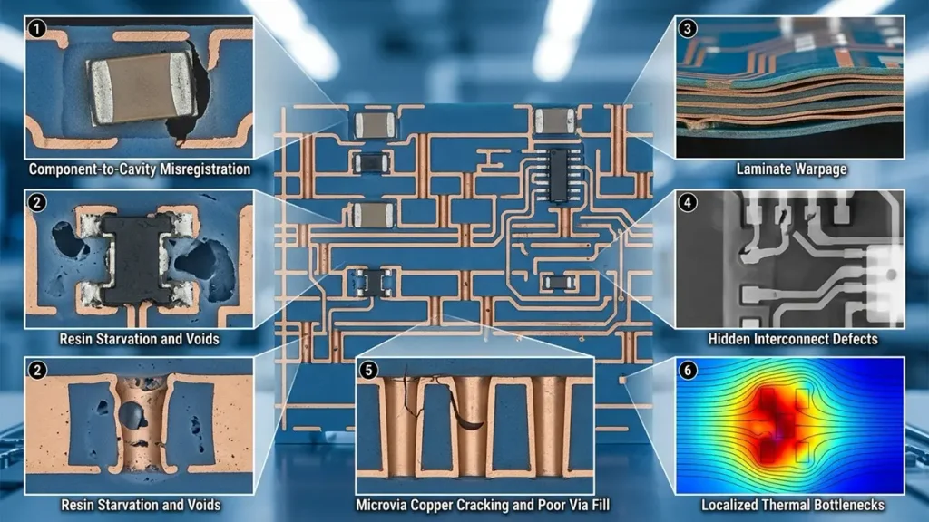
Embedded Component PCB Manufacturing Failure Risks and Defect Analysis
The highest-risk failures occur where a hidden component, a moving dielectric, and a later drilling or routing operation share the same datum. These risks must be managed as a connected process rather than as isolated PCB operations.
| Manufacturing pain point | Failure mechanism | Control expected from supplier |
|---|---|---|
| Component-to-cavity misregistration | Placement error or datum shift leaves insufficient dielectric margin or blocks a via | Vision alignment, fiducials tied to internal targets, X-ray verification, recorded capability |
| Resin starvation or excess flow | Cavity geometry and copper imbalance produce voids, resin squeeze-out, or local thickness error | Press recipe DOE, resin-flow model, copper balancing, cross-section coupons |
| Laminate warpage | Asymmetric copper, CTE mismatch, and embedded mass create bow/twist | Symmetric stack-up, controlled press profile, post-lamination measurement |
| Hidden solder/interconnect defects | AOI cannot see internal joints after lamination | X-ray/CT where suitable, electrical daisy chains, microsections, sample destructive analysis |
| Microvia cracks or poor fill | Laser residue, poor desmear, trapped gas, or inadequate plating causes opens after cycling | Laser energy window, desmear verification, metallographic cross-section, IST or thermal cycling |
| Fine-line over-etch and plating growth | Trace geometry changes with copper thickness, etch compensation, and plating current density | LDI compensation, mSAP process control, SPC on line/space and copper thickness |
| Thermal bottleneck | Embedded active device has no direct heat path to a plane or heat spreader | Thermal simulation, thermal vias/metal features, die attach and material review |
| Prototype-to-volume yield loss | Prototype uses manual selection or relaxed inspection that cannot scale | Pilot lot with production tooling, first-pass yield, defect Pareto, process capability report |
How should engineers design cavities and stack-ups for embedded components?
Design the cavity from the actual component tolerance envelope and lamination behavior, then reserve electrical, mechanical, and thermal clearances independently. A cavity is not simply a rectangular hole equal to the component outline.
For each embedded part, document: body X/Y/Z dimensions; terminal locations; coplanarity; maximum tilt; keep-out to copper and vias; adhesive or dielectric thickness; resin-flow direction; pressure exposure; thermal path; inspection datum; and whether the part is allowed to move during lamination.
Engineering practice: keep high-current or heat-generating embedded parts adjacent to a defined copper heat-spreading path, avoid placing a cavity across a mechanically weak via field, and balance copper around large openings. When a component is close to a controlled-impedance pair, model the local dielectric discontinuity; do not assume the nominal stack-up remains valid through the cavity region.
How do HDI, laser drilling, and mSAP improve embedded PCB density?
HDI microvias recover routing area around embedded components, while LDI and mSAP control fine geometries that conventional subtractive etching may not hold at comparable density. Their benefit is realized only when registration, plating, and inspection remain stable at the selected panel scale.
LDI removes phototool scaling from the exposure step and supports layer-specific compensation. UV and CO₂ lasers can be selected according to dielectric and copper structure; UV is useful for smaller, more localized features, while CO₂ systems are widely used for dielectric ablation. mSAP is valuable for thin base copper and fine traces, but the design must account for seed-layer removal, sidewall profile, plating overgrowth, and copper-thickness variation.
Current public capability data illustrate why the number must be qualified: one manufacturer reports 50/50 µm mSAP production geometry with 8–12 µm copper, while another reports 8/8 µm for advanced IC-substrate-class production. These are not interchangeable claims for an embedded PCB; request the process stack and evidence for your exact design.
How can hidden embedded structures be inspected and electrically tested?
Use a layered inspection plan: AOI for exposed circuitry, X-ray or CT where the feature is imageable, dimensional and registration measurement, cross-section coupons, continuity/isolation testing, and application-specific reliability testing.
| Inspection stage | What it verifies | Evidence to request |
|---|---|---|
| Incoming component inspection | Part identity, dimensions, tolerance, coplanarity, electrical value | Lot traceability and sampling plan |
| Pre-lamination placement | X/Y position, orientation, cavity clearance | Vision alignment record and placement map |
| Post-lamination X-ray/CT | Internal position, gross voids, solder/part condition where contrast permits | Image criteria and reject limits |
| Microsection | Copper thickness, via fill, cracks, resin fill, registration | Annotated cross-section from representative coupons |
| AOI/LDI verification | Outer-layer defects and fine-line registration | SPC trend and defect classification |
| Electrical test | Opens, shorts, resistance, embedded network function | Netlist-controlled test report |
| Reliability validation | Interconnect and material endurance under use conditions | Cycle profile, sample size, failures, and disposition |
No single inspection method sees every embedded defect. X-ray can expose hidden voids or alignment conditions in suitable geometries, but microsectioning remains direct evidence for metallization and resin interfaces. IPC-7092 emphasizes establishing inspection, testing, and reliability validation for embedded circuitry.
Which reliability tests are appropriate for high-density embedded component PCBs?
The test matrix should combine electrical continuity, microsection evidence, thermal cycling, humidity or temperature-humidity exposure, solderability where surface assembly remains, and interconnect stress testing selected for the actual material and application.
| Risk | Suggested validation | Typical engineering output |
|---|---|---|
| Via fatigue and CTE mismatch | Thermal cycling or IST on representative coupons | Resistance change, cycles to failure, failure cross-sections |
| Embedded joint fatigue | Thermal cycling with in-situ resistance where possible | Open-event log, X-ray before/after, metallographic evidence |
| Moisture degradation | Temperature-humidity exposure, insulation resistance | Insulation resistance trend and delamination inspection |
| Thermal performance | Thermal simulation plus powered thermal test | Junction/board temperature, thermal resistance, hotspot map |
| Mechanical integrity | Bend, shock, vibration, or board-level test as required | Warpage, cracks, electrical continuity after stress |
| High-speed performance | TDR/VNA coupon measurement and insertion-loss characterization | Impedance, insertion loss, return loss, and limit comparison |
Published industry test guidance commonly uses -40 °C to +125 °C thermal cycling, with 500–1,000 cycles selected according to application severity; the exact requirement must come from the customer qualification plan and applicable standard, not from a universal promise.
Which real-world applications justify embedded component PCB manufacturing?
Embedding is justified when the recovered surface area, shortened interconnect, thermal/electrical performance, or assembly reduction outweighs the added process and inspection cost.
| Application scene | Why embedding helps | Manufacturing attention |
|---|---|---|
| Automotive radar or control module | Reduces surface crowding and can shorten RF or sensor interconnects | Temperature cycling, vibration, dielectric stability, traceability |
| Medical handheld or monitoring device | Fits a constrained enclosure and protects selected passive networks | Moisture, cleaning exposure, repair policy, patient-safety documentation |
| Aerospace sensor electronics | Improves packaging density and can reduce external part count | Class 3 documentation, thermal/mechanical qualification, lot control |
| 5G/RF front-end module | Controls selected parasitics and preserves routing space | Low-loss material, copper roughness, impedance and RF test coupons |
| AI/HPC power or interconnect module | Supports dense power-integrity structures and advanced packaging transitions | Heat spreading, low inductance, high-current copper, warpage and microvia reliability |
| Industrial IoT sensor node | Reduces enclosure size and assembly operations | Cost/yield balance, field repair strategy, environmental reliability |
Scenario example: if a sensor module has a 30 mm × 25 mm usable board area and six decoupling parts consume two routing corridors, moving only the qualified capacitors into an internal structure may recover routing—not necessarily reduce the board outline. The engineering win may be one fewer HDI build-up layer or a larger connector keep-out, which can be more valuable than a headline percentage of size reduction.
How should procurement compare embedded component PCB suppliers?
Compare demonstrated process capability, yield, inspection evidence, engineering response, and total cost—not just the quoted unit price or the smallest advertised line/space.
| Supplier qualification question | Minimum evidence to request |
|---|---|
| Have you manufactured the same component class? | Anonymized cross-section, process flow, sample drawing, or customer-approved evidence |
| Can you support the required density? | Line/space, copper thickness, via stack, panel size, registration data, and yield |
| How are hidden features inspected? | X-ray/CT capability, microsection plan, electrical test coverage, and acceptance limits |
| Can prototype become volume production? | Pilot-lot plan, production equipment list, capacity, FAI, and process-control plan |
| What is the total cost? | Tooling, engineering, components, scrap/yield assumption, testing, logistics, and lead time |
| Who owns DFM decisions? | Named engineering contact, review checklist, revision control, and approval workflow |
Use total cost of ownership: unit price + tooling + engineering + component procurement + inspection + expected scrap + logistics + qualification. A low quote with an unreported yield penalty is not a low-cost supply chain.
What should a buyer include in an embedded component PCB RFQ?
Send a controlled RFQ package that lets the fabricator price the real process rather than infer critical requirements from Gerber files alone.
- Gerber or ODB++/IPC-2581 data, including cavity and embedded-component layers.
- Complete BOM with manufacturer part number, package drawing, body tolerance, Z-height, terminal finish, and electrical tolerance.
- Released stack-up with dielectric targets, copper weight/finished thickness, impedance requirements, and material family.
- Component placement map tied to board and layer datums, plus cavity dimensions and keep-outs.
- Via definition: laser diameter, target land, fill requirement, stacked/staggered rule, and back-drill policy where applicable.
- Surface finish, soldermask, dimensional tolerance, warpage limit, Class 2/Class 3 expectation, and cleanliness requirements.
- Inspection and qualification matrix: AOI, X-ray/CT, cross-section, electrical test, thermal cycling, humidity, IST, RF or thermal tests.
- Prototype quantity, pilot quantity, annual volume, delivery milestones, approved alternates, and change-control requirements.
Why should buyers evaluate Shenzhen Hongda Circuit Technology for this process?
Shenzhen Hongda Circuit Technology Co., Ltd. can be evaluated as an integrated advanced-PCB manufacturing partner when the project requires HDI, fine-line imaging, laser drilling, mSAP-related structures, sequential lamination, automated inspection, and engineering-led DFM.
The supplied company capability information identifies LDI, Mitsubishi UV/CO₂ laser drilling, advanced laser processing, mSAP fine-line fabrication, HDI microvias, automated plating, AOI, and X-ray inspection as relevant manufacturing resources. These capabilities are process enablers, not automatic proof that every embedded design is qualified. Hongda’s quotation should therefore be tied to a project-specific DFM review, capability coupon, inspection plan, and reliability report.
Our engineering recommendation is to start with a controlled feasibility build: freeze the component library, approve the cross-section, define the cavity and press DOE, measure registration before drilling, inspect hidden structures, and compare prototype data with a pilot lot. This approach prevents the common failure mode in which a visually successful prototype cannot meet volume yield or thermal-cycle requirements.
Contact Shenzhen Hongda Circuit Technology Co., Ltd. with the RFQ package for a manufacturability review and quotation. Ask for a written response covering process route, assumed tolerances, inspection coverage, material availability, prototype timing, volume lead time, and qualification deliverables.
What are the five most important supplier-search FAQs for procurement teams?
What line/space, microvia, and registration values can you guarantee in production?
Request the value at the specified copper thickness, layer count, board size, panel utilization, surface finish, and expected yield. Do not accept a brochure minimum without a cross-section or capability coupon.
How do you inspect components that are buried after lamination?
Ask for the exact X-ray/CT coverage, electrical test method, cross-section sampling plan, void and alignment criteria, and the procedure for nonconforming internal features.
What reliability data do you provide for embedded components and microvias?
Request the thermal-cycle profile, cycle count, sample size, monitoring method, failure criteria, IST or equivalent data, humidity testing, and post-test microsections.
What must be included in our RFQ, and can you support prototypes through mass production?
Provide ODB++/Gerber, BOM, component drawings, stack-up, cavity layers, impedance, testing, quantity, and application conditions. Ask the supplier to state prototype lead time, pilot controls, volume capacity, MOQ, and the process used to transfer the design into production.
Editorial note: Numeric values in this page are engineering starting points or publicly reported capability examples. Final acceptance criteria must be agreed in the drawing, purchase specification, capability study, and qualification plan for the specific product.
Sources used for standards and capability context: IPC-7092A and IPC-2316 scope documents; public mSAP capability data; public reliability-testing guidance.
About Author
David Chen https://www.linkedin.com/in/pcbcoming
David Chen boasts an extensive professional background in PCBA manufacturing, PCBA testing, and PCBA optimization, with specialized expertise in high-precision PCBA fault analysis and rigorous PCBA reliability testing. The author has worked with high-layer-count server PCB fabrication, ultra-low-loss backplane stackups, and thermo-mechanical reliability optimization for AI infrastructure projects involving 112G and 224G PAM4 architectures. Skilled in complex circuit design and cutting-edge advanced PCB manufacturing processes, he delivers solutions that elevate product durability and performance across industrial applications. His technical articles focusing on PCBA manufacturing workflows and testing methodologies are widely cited by industry peers, research institutions, and technical platforms, solidifying his reputation as a recognized technical authority in the global circuit board manufacturing sector.