Ultra-Thin PCB Reliability: Warpage Control, Failure Mechanisms & Test Validation Methods
A 0.2 mm board does not fail the way a 1.6 mm board fails. The same copper-resin CTE mismatch that a standard board absorbs elastically becomes, at ultra-thin cross-sections, a dominant source of bow, twist, and latent microvia cracking. This guide is written for reliability engineers, NPI teams, and quality managers who already know what an ultra-thin PCB is and need to answer a narrower question: how do you prove — with data, not assumptions — that a sub-0.4 mm board will survive reflow, thermal cycling, and years of mechanical flexing in the field.
We will not re-cover material selection, layer-count classification, or supplier vetting checklists; those are addressed elsewhere. This page focuses exclusively on the reliability chain: why ultra-thin boards warp, how to quantify and control that warpage, the test matrix that validates it, the failure modes that show up when control fails, and the inspection techniques that catch them before they reach the field.
1. Why Ultra-Thin PCB Reliability Behaves Differently From Standard Boards
Every rigid PCB experiences thermal stress during lamination and reflow because copper and the FR-4 resin system expand at different rates. Copper’s coefficient of thermal expansion (CTE) sits near 17 ppm/°C; FR-4 in the z-axis runs 45–70 ppm/°C below Tg and considerably higher above it. In a 1.6 mm, 8-layer board, this mismatch is distributed across enough dielectric volume and structural thickness that the resulting stress is mostly absorbed internally.
Thin that same construction to 0.35 mm and the physics does not scale linearly. Bending stiffness scales with the cube of thickness, so cutting thickness by a factor of 4–5× reduces stiffness by roughly two orders of magnitude. The identical CTE mismatch now has to be absorbed by a structure with a fraction of the resistance to deformation — the result is measurable bow, twist, and, in marginal designs, delamination or trace fracture at the flex-to-rigid transition. Reliability engineering on ultra-thin boards is therefore not “the same checklist at a smaller scale”; it is a distinct discipline built around three questions this guide answers in order: what causes the deformation, how is it controlled and measured, and how is long-term survivability proven under test.
2. Root Cause Analysis: The Mechanics of Warpage in Sub-0.4 mm Boards
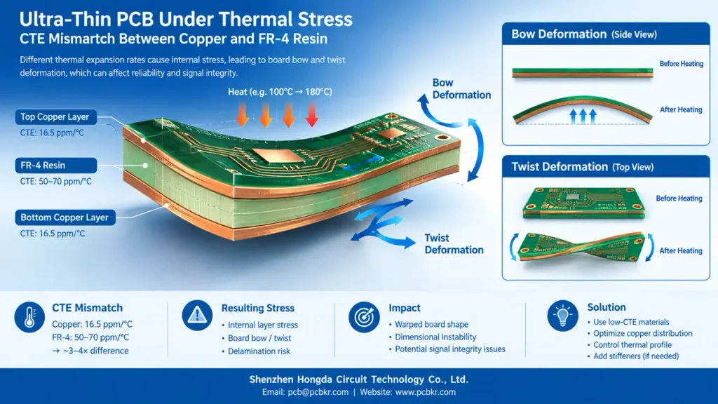
Ultra-Thin PCB Warpage and CTE Mismatch Mechanism
2.1 The CTE Mismatch Model
Warpage in a multilayer laminate is driven by the bimetallic-strip effect, extended across N layers of alternating copper and resin. Each copper layer wants to contract at ~17 ppm/°C on cooldown from lamination or reflow peak; each resin layer wants to contract at 45–70 ppm/°C (below Tg) or considerably more above Tg, where the resin transitions from glassy to rubbery and its CTE can jump 3–4×. Because copper and resin are bonded, the layer with the lower CTE constrains the layer with the higher CTE, generating internal shear stress at every copper-resin interface.
For a symmetric, balanced stack-up this stress is largely self-cancelling because equal moments act on both sides of the neutral axis. For an asymmetric stack-up — uneven copper weight top-to-bottom, an off-center core, or a solder mask applied to only one side — the moments do not cancel, and the panel bows toward the side with lower net CTE (typically the heavier-copper side, which resists more).
Engineering approximation: bow depth scales approximately with (ΔCTE × ΔT × L²) / (8 × t), where L is panel span and t is board thickness. Because t appears in the denominator, halving thickness roughly doubles bow for an identical copper-imbalance and thermal delta — this is the single most important relationship for ultra-thin DFM.
2.2 Residual Stress: Lamination vs. Reflow
Two independent stress events stack on ultra-thin boards, and treating them as one is a common root-cause miss during failure analysis.
- Lamination residual stress: introduced during the press cycle as the stack cools from ~180–220°C cure temperature to ambient under mechanical constraint (press platens, pins). This stress is “baked in” and present in the bare board before any component is soldered.
- Reflow-induced stress: superimposed during SMT, as the board ramps to a 235–260°C peak (lead-free profiles) and back. Because this second thermal excursion often approaches or exceeds resin Tg, the board can transiently lose a significant fraction of its flexural modulus, allowing residual lamination stress to release as visible bow — which is why boards that measure flat off the fab line can warp only after SMT reflow.
Root-cause investigations that measure flatness only at incoming QC and not post-reflow routinely miss this interaction. A board can pass IPC-6012 flatness on the fab floor and still exceed SMT placement tolerance after a single reflow pass.
2.3 Copper Balance and Stack-Up Symmetry — Quantified
“Keep the stack-up symmetric” is the standard guidance; the reliability-critical detail is how much asymmetry a given thickness class can tolerate before bow exceeds spec. As a working DFM rule for 4-layer ultra-thin construction at 0.35 mm:
| Copper Weight Imbalance (L1 vs L4) | Typical Additional Bow | Design Action |
| < 10% difference | Negligible (within noise of measurement) | Acceptable as-is |
| 10–25% difference | +0.1–0.3% bow | Add copper thieving on the lighter layer to close the gap |
| > 25% difference | +0.4–0.8% bow, often exceeding 0.75% limit | Redesign layer assignment or mirror copper pour before tooling release |
Copper thieving (dummy copper fill on sparsely-routed layers) is the primary lever engineers control post-layout. The target is not zero imbalance — that is rarely achievable with real circuitry — but keeping per-layer copper weight within roughly 15% of the mirrored layer, verified during DFM review before the panel is tooled, not after first-article inspection flags a bow failure.
3. Warpage Measurement and Process-Level Control
3.1 IPC-TM-650 Method 2.4.22 — The Reference Test
IPC-TM-650 Method 2.4.22 is the standard bow-and-twist measurement referenced by IPC-6012 acceptance criteria. The method places the board on a flat reference surface and measures the maximum deviation of the board surface from that plane, expressed as a percentage of the diagonal (bow) or the relevant dimension (twist).
- Bow (%) = (maximum deviation from flat / diagonal length of the board) × 100
- IPC-6012 Class 2/3 SMT assembly threshold: ≤ 0.75% for boards intended for surface-mount reflow; some ultra-thin high-density designs specify tighter internal limits of 0.5% to build in margin for post-reflow relaxation.
- Measurement is typically performed both post-fabrication (bare board) and, for reliability qualification, post-reflow simulation — running the board through a representative reflow profile before re-measuring, since section 2.2 shows these two numbers are not interchangeable.
For boards under approximately 0.6 mm, non-contact optical or laser flatness scanning is preferred over mechanical dial-gauge methods, because contact probes can locally deflect a thin, low-stiffness panel and introduce measurement artifact. A full-panel laser scan also produces a flatness map rather than a single worst-point number, which is far more useful for tracing bow back to a specific stack-up asymmetry or lamination zone.
3.2 Lamination Process Parameters That Drive Flatness
Vacuum lamination is necessary but not sufficient; the pressure and temperature ramp profile determines whether residual stress is minimized or locked in.
| Process Variable | Effect on Ultra-Thin Warpage | Typical Control Range |
| Heating ramp rate | Fast ramps create through-thickness thermal gradients that cure resin unevenly, locking in asymmetric stress | 1.5–2.5°C/min for sub-0.4 mm builds (slower than standard-thickness recipes) |
| Peak pressure application timing | Applying full pressure before resin reaches gel point can squeeze out resin unevenly across a thin, flexible panel | Staged pressure ramp, full pressure only after resin viscosity minimum is passed |
| Cooling ramp rate | Rapid cooling under constraint freezes in higher residual stress than a controlled ramp | ≤ 3°C/min through the Tg transition band |
| Press dwell at peak temperature | Insufficient dwell leaves incomplete cure and post-cure shrinkage after unloading | Per resin system data sheet, typically not shortened for thin builds despite lower thermal mass |
Zone-controlled press platens (rather than single-zone presses) allow the pressure and temperature profile to be tuned independently across the panel area, which matters more as panel size grows relative to thickness — a large-format thin panel is far more prone to edge-versus-center thermal lag than a small one.
3.3 Panel Handling as a Warpage Contributor
Warpage is not only introduced at lamination. Mechanical handling of an unsupported thin panel — standard conveyor rollers, gravity sag during vertical storage, or stacking without separators — can introduce permanent set, particularly above Tg during any subsequent thermal step. Vacuum carrier fixtures during imaging, etching, and AOI, combined with tab-routing on support rails through final singulation, prevent this secondary, process-induced warpage from being conflated with lamination-stage warpage during failure analysis.
4. Reliability Test Matrix for Ultra-Thin PCBs

Ultra-Thin PCB Reliability Test Matrix & Validation Methods
A complete ultra-thin reliability qualification plan combines four test families. None of them substitutes for another — a board that passes thermal cycling can still fail bend-life testing, and a board with acceptable flatness can still fail CAF testing under bias-humidity.
4.1 Thermal Cycling
Thermal cycling validates the CTE-mismatch stress discussed in Section 2 under repeated, not single-pass, thermal excursion — the condition closest to field operation for automotive and industrial applications.
| Parameter | Typical Ultra-Thin Test Condition |
| Temperature range | -40°C to +125°C (consumer/industrial); -40°C to +150°C (automotive under-hood) |
| Ramp rate | 10–15°C/min, air-to-air chamber |
| Dwell time at extremes | 15–30 minutes, sufficient for full board thermal saturation given low thermal mass |
| Cycle count | 500 cycles (consumer), 1,000 cycles (automotive ADAS per IATF 16949 program requirements), 1,500+ for medical implantables |
| Failure criteria | Electrical continuity/resistance shift > 10%, visible delamination, microvia resistance drift, or bow exceeding post-test flatness limit |
Because ultra-thin boards have lower thermal mass than standard boards, they equilibrate to chamber temperature faster — this is favorable for cycle throughput but means dwell time should be verified by thermocouple instrumentation on a representative unit rather than assumed from standard-board profiles.
4.2 Bend / Flex-Life Cycling (Flexible and Rigid-Flex Constructions)
For polyimide or LCP-based flexible sections, and for rigid-flex hybrids, static thermal stress is only part of the reliability picture; dynamic mechanical fatigue at the bend radius is often the dominant field failure mode.
- Bend radius specification: typically expressed as a multiple of laminate thickness (e.g., 6× thickness for dynamic flex, 10× for static installation flex) — tighter radii sharply reduce fatigue life.
- Cycle count targets: 10,000–50,000 cycles for consumer dynamic-flex applications (hinges, sliding mechanisms); 100,000+ cycles for wearables and robotic joints expected to flex continuously over a multi-year service life.
- Test fixture: a reciprocating bend-test jig cycling the flex section through the specified radius at a controlled rate (commonly 0.5–2 Hz), with continuous continuity monitoring on the traces under test rather than end-of-test inspection only, since intermittent opens during flex are easy to miss with a static post-test check.
- Failure criteria: resistance increase beyond a defined threshold (commonly 5–10% for signal traces) sustained across multiple consecutive cycles, distinguishing a genuine developing fracture from momentary contact noise.
4.3 Humidity and Bias-Humidity Testing (THB / HAST / CAF Screening)
Ultra-thin constructions have proportionally less dielectric thickness between adjacent conductors and between layers, which shortens the diffusion path for moisture ingress and the conductive path length available for CAF growth (see 5.1). This makes bias-humidity testing disproportionately important relative to standard-thickness boards, even though the underlying test methods are shared industry standards.
| Test | Typical Condition | What It Validates on Ultra-Thin Boards |
| THB (Temperature-Humidity-Bias) | 85°C / 85% RH, DC bias applied, 500–1,000 hrs | Long-duration moisture ingress and CAF initiation under realistic field bias |
| HAST (unbiased or biased) | 130°C / 85% RH or 110°C / 85% RH, biased, 96–264 hrs | Accelerated equivalent of THB — used when program schedule cannot absorb full THB duration |
| Pre-conditioning moisture bake | 125°C bake per J-STD-020 moisture sensitivity level, prior to reflow simulation | Confirms laminate (especially polyimide, which is hygroscopic) is fully dried before thermal stress, preventing steam-driven delamination during reflow |
4.4 Test Sequencing
The order in which these tests are applied matters for a qualification build: standard practice is pre-conditioning bake, followed by reflow simulation (2–3 passes) to capture the stress interaction described in 2.2, followed by thermal cycling, followed by bias-humidity testing, with electrical and flatness measurement checkpoints between each stage rather than only at the end. This sequencing surfaces which stage introduces a given failure mode, which is essential for root-cause corrective action rather than a pass/fail result alone.
5. Failure Mode Deep Dive
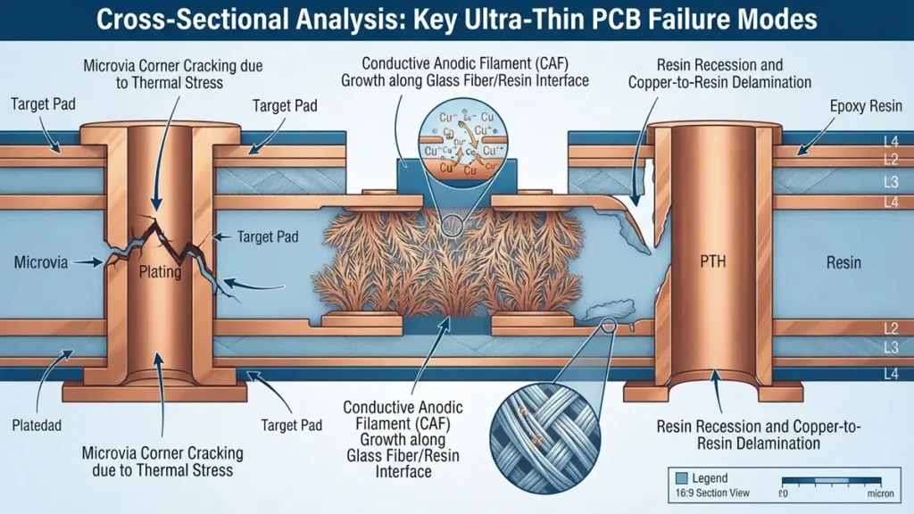
PCB Failure Modes: CAF, Microvia Cracking & Resin Recession
5.1 Conductive Anodic Filament (CAF) Growth
CAF is the electrochemical growth of a copper-containing filament along a fiber-glass/resin interface, driven by moisture, ionic contamination, and an applied electric field between adjacent conductors of opposite potential. It is a subsurface failure — invisible externally — that manifests as a gradual insulation resistance drop and eventual short.
- Why it is disproportionately relevant to ultra-thin boards: CAF growth rate is a function of conductor spacing and the length of the fiber/resin interface path between them. Thinner dielectrics and finer pitch (a near-universal feature of ultra-thin, high-density designs) reduce the path length a filament must bridge to cause a short.
- Detection: CAF is confirmed destructively via microsectioning along the suspect conductor pair, or non-destructively screened via insulation resistance (IR) trending during THB/HAST — a gradual IR decline over test duration, rather than a sudden drop, is the characteristic CAF signature.
- Mitigation levers: CAF-resistant laminate weave styles (spread-tow or flat glass constructions reduce resin-starved fiber junctions), adequate hole-to-trace and trace-to-trace clearance at the design stage, and controlled drilling to avoid glass-fiber wicking/smear that creates a pre-existing moisture path.
5.2 Microvia Barrel Cracking and Resin Recession
In ultra-thin HDI constructions with stacked or staggered microvias, the dominant thermal-cycling failure mode is not the plated barrel itself fracturing outright on the first cycle, but incremental fatigue at the via corner — the transition from the via barrel to the target pad — where stress concentrates due to the geometric discontinuity.
- Contributing factors specific to thin dielectrics: a thinner dielectric between layers means a shorter, stiffer via with less compliance to absorb z-axis CTE expansion, concentrating strain at the corner interface rather than distributing it along a longer barrel.
- Resin recession: repeated thermal cycling above Tg can cause localized resin softening and creep away from the via wall, reducing copper-to-resin adhesion and accelerating corner crack initiation on subsequent cycles — this is why cumulative cycle count, not single-pass reflow, is the meaningful qualification metric.
- Detection: cross-sectional microscopy remains the definitive method; for production screening without destructive sectioning, four-point resistance measurement of via chains (daisy-chained microvia test coupons) trended across thermal cycling detects incremental resistance drift before a full open occurs.
5.3 Delamination and Copper Foil Fracture
Delamination on ultra-thin boards most commonly initiates at the flex-to-rigid transition zone in rigid-flex constructions, or at high-copper-density regions adjacent to sparse-copper regions in rigid builds, where the local CTE mismatch and stress concentration described in Section 2 are most severe.
- Root causes: inadequate pre-bake before reflow (moisture flashing to steam and delaminating layers), insufficient lamination pressure dwell at the resin flow point, or contamination at the copper-resin interface prior to lamination.
- Copper foil fracture: distinct from delamination, this is a mechanical crack through the copper itself, typically at a sharp internal corner (trace-to-pad transition, or a via-in-pad structure without adequate fillet) subjected to repeated flex or thermal strain. HTE (high-temperature elongation) foil is specified over standard electrodeposited foil specifically because its higher elongation-at-break tolerates more strain before cracking — relevant foil selection criteria for reliability, not just conductivity.
- Detection: acoustic microscopy (C-SAM) is the preferred non-destructive method for delamination screening across a full panel, since it detects the density discontinuity at a delaminated interface without cross-sectioning every sample.
6. Inspection and Verification Techniques
6.1 X-Ray Void and Void-Density Analysis
3D X-ray inspection (e.g., computed tomography or oblique-angle X-ray) is used on ultra-thin boards primarily for two reliability-relevant checks: void content within microvia barrels (voiding reduces the effective cross-section carrying current and thermal-fatigue stress, accelerating the failure mode in 5.2) and PTH/via fill quality in stacked-via structures where an internal void is otherwise undetectable without destructive sectioning. Acceptance criteria commonly reference IPC-6012 void limits, with tighter internal thresholds applied for automotive and medical programs.
6.2 Cross-Sectional (Microsection) Analysis
Destructive cross-sectioning remains the ground-truth method for confirming CAF presence, microvia corner cracking, resin recession, and delamination extent, because it directly reveals the physical interface condition that non-destructive methods can only infer. Standard practice on ultra-thin reliability qualification builds is to pull cross-section coupons at defined test-sequence checkpoints (post-reflow, mid-cycle, end-of-test) rather than only at final failure, so the progression of a failure mode — not just its endpoint — is documented.
6.3 Electrical Test Limitations on Thin, Fine-Pitch Boards
Flying-probe and AOI remain necessary for opens/shorts and cosmetic defect screening, but neither is sufficient alone for reliability validation on ultra-thin boards: flying-probe verifies point-to-point continuity at time of test but cannot detect an incrementally-developing microvia crack that has not yet opened the circuit, and AOI inspects surface geometry, not subsurface CAF or delamination. This is why the test matrix in Section 4 layers destructive and accelerated-life methods on top of standard electrical test rather than relying on electrical test as a reliability proxy.
7. High-Speed Signal Reliability Under Thermal and Mechanical Stress
For ultra-thin boards carrying high-speed serial links (112–224 Gbps PAM4-class channels), reliability and signal integrity are coupled rather than independent concerns. A design that meets initial insertion-loss and impedance targets at time-zero can drift out of spec after thermal cycling if the underlying mechanical degradation modes in Section 5 are present.
- Impedance drift from dielectric thickness variation: because dielectric thickness directly sets characteristic impedance on a thin stripline or microstrip, any resin recession or delamination-driven local thickness change (5.2, 5.3) produces a measurable impedance shift, not just a mechanical defect — tying signal-integrity test coupons into the thermal-cycling and bend-life test plan, not just initial production test, is standard practice for these programs.
- Post-stress verification: impedance (TDR) and insertion-loss (VNA) measurement on dedicated test coupons repeated after thermal cycling and, for flex constructions, after bend-life cycling, confirms the channel still meets its budget at end-of-test, not only at time-zero shipment.
- Via stub and corner-crack interaction: an incrementally cracking microvia corner (5.2) increases contact resistance before it opens the circuit entirely — at multi-GHz frequencies this resistance increase manifests as an insertion-loss anomaly at a specific frequency band well before a DC continuity failure would be flagged, making swept-frequency measurement a more sensitive early-warning tool than DC resistance alone for high-speed channels specifically.
8. Reliability Design and Qualification Checklist
A practical, stage-gated checklist for engineering teams sourcing or qualifying an ultra-thin PCB, organized by when in the program each item should be verified.
8.1 At DFM Review (Before Tooling)
- Verify copper weight balance layer-to-layer is within the imbalance thresholds in Section 2.3, with thieving/dummy fill specified where needed.
- Confirm stack-up symmetry about the centerline, including solder mask and any asymmetric surface finish application.
- Review microvia and via-in-pad structures for corner geometry and stub length against the fatigue mechanism in 5.2.
- Confirm trace-to-trace and hole-to-trace clearances meet CAF-resistant design margins for the laminate weave style specified, not just minimum electrical clearance.
- For flex/rigid-flex sections, confirm bend radius against the dynamic vs. static flex requirement (see pillar-page guidance on rigid vs. flex selection) and specify HTE or equivalent high-elongation foil in flex zones.
8.2 At First Article / Qualification Build
- Measure bow and twist per IPC-TM-650 2.4.22 both as-fabricated and after a representative reflow simulation (2–3 passes).
- Pull cross-section coupons at zero-hour to confirm baseline via, plating, and interface quality before stress testing begins.
- Run the full test sequence in Section 4.4 (pre-condition bake → reflow simulation → thermal cycling → bias-humidity) with checkpoint measurements between stages, not only pass/fail at the end.
- For high-speed designs, baseline TDR/insertion-loss on signal-integrity coupons before stress and repeat after each major test stage per Section 7.
8.3 Data to Request From Any Ultra-Thin PCB Supplier
- Flatness data (2.4.22) by lot, not a single qualification-sample data point — lot-to-lot process variation is where production reliability risk actually lives.
- Cross-section reports from the qualification build showing via and interface condition, not just a certificate of conformance.
- CAF and thermal-cycling test reports specific to the laminate and copper weight combination in your design, since these are construction-specific results, not generic material-family claims.
- For flex/rigid-flex programs, bend-life test data at the specific radius and cycle count relevant to your application’s duty cycle, not a generic flex-life figure quoted for a different construction.
9. Summary
Ultra-thin PCB reliability is governed by a chain that starts with a measurable, controllable physical cause — CTE-driven residual stress amplified by low bending stiffness — and ends in specific, named failure modes (CAF, microvia corner cracking, delamination, copper fracture) that each have a corresponding detection method and design lever. Treating reliability qualification as a single pass/fail thermal-cycling report misses the interactions this guide has walked through: lamination stress that only releases after reflow, impedance drift that originates in a mechanical degradation mode, and CAF growth that is invisible until insulation resistance trending reveals it. A qualification plan built around the sequenced test matrix in Section 4, verified with the inspection techniques in Section 6, and checked against the DFM and data-request checklist in Section 8, is what actually de-risks an ultra-thin design before it reaches volume production.
Frequently Asked Questions
How do suppliers ensure the flatness (warpage control) of sub-0.4 mm ultra-thin PCBs after SMT reflow?
Excellent suppliers evaluate copper weight balance (layer-to-layer symmetry) during the DFM stage, recommending that the copper weight difference between L1 and L4 be kept within 15%, while utilizing copper thieving in sparse areas. Simultaneously, suppliers should use slow heating ramps (1.5–2.5°C/min), staged pressure control, and a controlled cooling rate ($\le$ 3°C/min) to eliminate internal stress, and provide post-reflow simulated IPC-TM-650 flatness scanning data.
Do suppliers have the capability to perform microvia and flex-zone fatigue testing for ultra-thin HDI and rigid-flex boards?
One of the core pain points of ultra-thin boards is microvia barrel fatigue cracking and dynamic bending failure in flex zones. Buyers should verify whether suppliers execute rigorous dynamic bend-cycling tests (e.g., 10,000 to 50,000+ cycles) during the qualification build phase, and specify HTE (high-temperature elongation) copper foil to enhance strain tolerance.
What process and material controls do suppliers implement to prevent Conductive Anodic Filament (CAF) growth?
Given that ultra-thin boards feature thinner dielectrics and shortened insulation clearances, CAF risk increases significantly. Qualified suppliers should select CAF-resistant laminate weave styles (such as spread-tow or flat glass constructions), tightly control drilling processes to avoid glass-fiber wicking or smearing, and provide rigorous THB (Temperature-Humidity-Bias) or HAST test data.
For high-speed applications like 112–224 Gbps PAM4, can suppliers guarantee signal integrity (SI) before and after thermal stress?
Resin recession or microscopic delamination induced by mechanical stress directly alters dielectric thickness, resulting in impedance drift. Buyers should look for suppliers who combine high-frequency testing (TDR impedance, VNA insertion loss) with thermal-mechanical stress testing (such as re-testing after thermal cycling) to ensure channel performance remains within budget under extreme conditions.
What reliability data packages and shipping reports should buyers typically request when purchasing ultra-thin PCBs?
Ultra-thin PCB quality cannot be evaluated solely on a Certificate of Conformance (C of C). Quality suppliers should be able to provide:
Lot-specific flatness data (Bow & Twist reports measured per IPC-TM-650 2.4.22);
Zero-hour and post-test microsection reports evaluating via, microvia corner, and interface quality;
CAF and thermal-cycling test reports specific to the laminate and copper weight combination used in the design.
About Author
David Chen https://www.linkedin.com/in/pcbcoming
David Chen boasts an extensive professional background in PCBA manufacturing, PCBA testing, and PCBA optimization, with specialized expertise in high-precision PCBA fault analysis and rigorous PCBA reliability testing. The author has worked with high-layer-count server PCB fabrication, ultra-low-loss backplane stackups, and thermo-mechanical reliability optimization for AI infrastructure projects involving 112G and 224G PAM4 architectures. Skilled in complex circuit design and cutting-edge advanced PCB manufacturing processes, he delivers solutions that elevate product durability and performance across industrial applications. His technical articles focusing on PCBA manufacturing workflows and testing methodologies are widely cited by industry peers, research institutions, and technical platforms, solidifying his reputation as a recognized technical authority in the global circuit board manufacturing sector.