NPI PCB Manufacturing & Assembly: From Prototype to Production
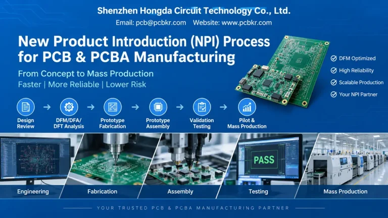
A qualified NPI PCB manufacturer takes a design from first prototype through DFM/DFA/DFT review, EVT/DVT/PVT builds, and a controlled handoff into volume production — usually compressing a 2–4 week fragmented cycle into 3–5 working days when fabrication, SMT assembly, and test sit under one roof. Shenzhen Hongda Circuit Technology Co., Ltd. runs this full chain in-house.
What Is NPI PCB Manufacturing?

NPI PCB High-Tech Manufacturing Facility
NPI (New Product Introduction) PCB manufacturing is the structured process of moving a circuit board design from schematic to a repeatable, yield-stable production line — it is not simply “making a prototype,” it is the engineering gate that determines whether a design can be built at volume without redesign.
Most procurement teams searching this term have already been burned by a supplier who treated NPI as a rush prototype order: five boards etched fast, shipped, and forgotten. That’s fabrication, not NPI. Real NPI work includes a documented DFM/DFA/DFT pass, a first-article inspection report, a controlled BOM with approved-vendor-list (AVL) alternates, and a defined criteria for graduating from EVT to DVT to PVT. At Hongda, every NPI job opens a traveler that follows the board from CAM engineering through final test — the same traveler a customer can audit six months later when they ask why a via failed in the field.
Manufacturing pain point: the most common failure we see in incoming NPI designs is a stack-up mismatch — the schematic assumes a controlled-impedance trace width calculated for a 4-layer, 1.6 mm board, but the fab drawing specifies a 6-layer, 1.0 mm stack. Left uncaught, this produces a ±15% impedance deviation on high-speed lines, which shows up as intermittent signal integrity failures during DVT — usually two to three weeks after the customer thought the design was locked.
How Does NPI PCB Production Differ From Standard Mass-Production PCB Manufacturing?

NPI PCB vs Mass Production Technical Comparison
NPI production runs smaller batches (typically 5–500 units per build stage) against a design that is still allowed to change, while mass production runs fixed panels (often 1,000+ units) against a frozen Gerber and BOM revision — the tooling, inspection sampling rate, and documentation requirements are structurally different, not just smaller versions of each other.
In mass production, we run 100% panel utilization with a locked stencil and a sampling AOI/ICT plan (often 1-in-10 or statistical process control). In NPI, we deliberately over-inspect: 100% AOI, 100% flying-probe electrical test, and manual first-article verification on every panel, because the goal isn’t throughput — it’s catching a design defect before it propagates into a $40,000 tooling run. Our NPI lines use short-run stencils (laser-cut, 0.12 mm thickness, step-down apertures for 01005 components) rather than the electroform stencils used in mass SMT, because tooling lead time on NPI orders needs to be 24–48 hours, not the 5–7 days electroform stencils require.
Scenario: a Shenzhen-based medical device customer sent us a 10-layer board with 0.1 mm minimum trace/space for an EVT build of 20 units. Because we run the same LDI (laser direct imaging) line for both NPI and mass production — rather than a separate “prototype shop” with lower-resolution phototool imaging — the EVT boards had identical etch-factor and copper-thickness tolerance to what the eventual 5,000-unit PVT run would produce. That single decision eliminated the re-spin that typically happens when a customer validates on a prototype board built on different equipment than the production line will use.
What Does an NPI Engineering Review (DFM/DFA/DFT) Actually Check?

NPI PCB DFM/DFT Verification and Review
DFM (Design for Manufacturability), DFA (Design for Assembly), and DFT (Design for Test) review checks roughly 40–60 discrete rule categories — annular ring size, copper-to-edge clearance, solder mask dam width, component-to-component spacing, test-point accessibility, and panelization tab placement — before a single panel is fabricated.
Our CAM engineers run Gerber files through Valor/Genesis-class DFM software first, then perform a manual second pass, because automated DFM catches geometric rule violations but misses process-specific risk — for example, a 0.15 mm annular ring might pass an automated rule check but still be marginal on our specific drill-to-copper registration tolerance (±0.05 mm on a 1.6 mm, 8-layer board). DFA review checks component orientation ambiguity (polarized parts without clear silkscreen reference), fine-pitch QFN thermal pad via count (we require a minimum of 9 thermal vias at 0.3 mm diameter under a 5×5 mm QFN to avoid voiding), and BGA ball-to-via keep-out for rework access. DFT review confirms every net has a probeable test point ≥0.6 mm diameter with ≥1.27 mm pitch for flying-probe access, since boards without test-point access cannot get 100% electrical coverage and must ship with only visual/AOI inspection — a real risk for safety-critical designs.
Manufacturing pain point: the single costliest DFA miss we catch is inadequate paste-to-pad ratio on 0.4 mm pitch QFN/BGA parts. A stencil aperture that is even 10% oversized relative to the pad on 0.4 mm pitch parts produces solder bridging at a rate that can exceed 8% of joints on a dense board — invisible until AOI or, worse, until the board fails in functional test three weeks later.
How Are PCB and PCBA Prototypes Built and Validated for NPI?
prototype validation for NPI runs on the same fabrication and SMT equipment used for production — not a separate “quick-turn” shop — with a formal first-article inspection (FAI) report covering dimensional, electrical, and visual criteria before the customer receives the units.
Our prototype turn time is 24–72 hours for bare PCB (2–8 layers) and 3–5 days for assembled PCBA, using the same laser drilling (for microvias down to 0.1 mm), LDI imaging, and Yamaha/Panasonic-class SMT placement equipment used on mass-production lines. Placement accuracy on our SMT lines runs ±0.025 mm (Cpk-verified), which matters directly for 0201 and 01005 component prototypes where pad size leaves almost no margin for placement drift.
Scenario: a customer developing an IoT sensor module needed 15 prototype units with a 0.3 mm BGA pitch and buried microvias. Because the boards were built on the production LDI and laser-drill line rather than a low-volume prototype process, the EVT units came back with drill registration within ±0.05 mm — tight enough that the customer’s DVT electrical test data carried forward directly into their production qualification report, saving roughly three weeks of re-validation.
How Is the BOM Validated and Are Components Sourced During NPI?
BOM validation cross-checks every line item against lifecycle status, RoHS/REACH compliance, footprint match to the Gerber/ODB++ data, and at least one approved alternate part number — because an unvalidated BOM is the single most common cause of NPI schedule slippage.
We run every incoming BOM through a component-lifecycle check (active / NRND / EOL / obsolete status) before quoting, because a part marked “active” on a datasheet from 2019 may already carry a 26–52 week lead time in 2026 due to fab allocation. For each critical part — MCU, PMIC, connector — we require the customer approve at least one form-fit-function alternate, sourced only from authorized distribution (not gray-market brokers), with full traceability documentation (date code, lot code, COC) retained for the life of the program.
Manufacturing pain point: the recurring issue we flag on 1 in roughly every 4 incoming BOMs is a footprint mismatch — the schematic symbol calls out a part number, but the PCB footprint was drawn from a different (often older) package revision of the same part. This passes visual review because the part “looks right” in the CAD tool, but produces open joints or tombstoning at SMT reflow. Our incoming BOM check overlays the manufacturer’s official footprint drawing against the customer’s Gerber pad geometry before assembly begins, not after the first failed board comes off the line.
What SMT and THT Assembly Capabilities Does NPI Require?
NPI PCB assembly needs a line that can run mixed SMT/THT in the same build without a separate setup change, handle components from 01005 up to large connectors and heatsinks, and requalify the reflow profile for each new stack-up — capabilities a pure high-volume line is often not configured to flex on quickly.
Our SMT lines support component range from 01005 (0.4×0.2 mm) to 45×45 mm QFP/BGA packages, with mixed-technology (SMT + selective-wave THT) capability in a single production flow. Reflow profiling is done per-board on an 8-zone or 10-zone oven with thermocouple-verified profiles (typical peak 245°C ±5°C for SAC305 lead-free paste, ramp rate ≤3°C/second to avoid component thermal shock), because a profile validated on a 1.6 mm 4-layer board will over- or under-heat a 3.2 mm 12-layer board with heavier copper — a detail that matters enormously on NPI where stack-up frequently changes between EVT and DVT.
Scenario: an automotive electronics customer’s EVT board used through-hole connectors alongside 0.5 mm pitch SMT ICs. Rather than routing the through-hole reflow through a separate subcontractor (a common bottleneck that adds 5–10 days per build cycle), our selective-wave soldering station handled the THT connectors in the same production run, keeping the full EVT turnaround inside 4 working days.
How Is NPI PCB Tested — AOI, Flying Probe, ICT, and X-Ray?
NPI boards should receive 100% AOI, 100% flying-probe or bed-of-nails electrical test where fixturing allows, and X-ray inspection on every BGA/QFN board — because sampling-based testing (common in mass production) is not statistically reliable on the small batch sizes typical of NPI.
AOI on our lines runs at sub-25 micron optical resolution, checking solder fillet geometry, component polarity, and presence/absence on every board. Flying-probe test achieves >99% net coverage on boards with adequate test-point design (see DFT section above) and typically adds only 3–8 minutes per panel at NPI volumes — a cost worth paying compared to shipping an electrically-unverified board. X-ray (AXI) inspection is mandatory on any board with BGA, QFN, or bottom-terminated components, since solder joint quality under these packages is not visible to AOI; our 5-axis X-ray systems can resolve voiding down to <10% of pad area on 0.4 mm pitch BGAs, which is the IPC-610 Class 2 acceptance threshold for many customers’ programs.
Manufacturing pain point: the most expensive test gap we see customers accept, usually to save cost on a “cheap” prototype quote, is skipping X-ray on BGA boards. A hidden solder void that AOI cannot see may function correctly at room-temperature bench test and still fail thermal cycling in the field — precisely the failure mode DVT/PVT testing exists to catch, but only if the inspection method can actually see the defect.
What Happens During EVT, DVT, and PVT Builds?
EVT (Engineering Validation Test) proves the design works electrically and mechanically at low volume (typically 10–50 units); DVT (Design Validation Test) proves the design is manufacturable and reliable at a build closer to production intent (100–500 units, often with tooling that will carry into mass production); PVT (Production Validation Test) proves the full production line — including operators, fixtures, and supply chain — can hit yield and cycle-time targets at near-full volume before mass production sign-off.
Each stage has a different exit criterion, and conflating them is a common source of schedule risk. EVT exit criteria: functional pass rate, no critical DFM/DFA issues open. DVT exit criteria: reliability test results (thermal cycling, HALT/HASS as applicable), yield ≥95% on the assembly line, all ECOs closed. PVT exit criteria: process capability data (Cpk ≥1.33 on key parameters), first-pass yield at target (commonly ≥98% for consumer electronics, higher for automotive/medical), and a signed production readiness review.
Scenario: a consumer electronics customer wanted to skip DVT and go straight from EVT to a 2,000-unit PVT run to save two weeks. We ran a limited DVT (75 units) instead, which surfaced a thermal-cycling-induced crack in a corner-mounted connector solder joint — a failure mode invisible in the 20-unit EVT batch because it only appeared statistically after ~150 thermal cycles. Catching it in a 75-unit DVT run cost four days; catching it in a 2,000-unit PVT run would have cost the full tooling and material cost of the run plus a field-failure risk.
How Does Production Transfer From NPI to Mass Production Work?
production transfer means moving a validated design from the NPI line to the mass-production line with zero unplanned process changes — the same stencil design intent, the same reflow profile family, the same AVL — so that PVT test data remains valid evidence for the mass-production process, not just the prototype process.
Because our NPI and mass-production lines share the same fabrication and SMT equipment platform (rather than NPI running on separate “prototype-grade” machines), transfer means scaling panel utilization and cycle time, not requalifying the process from zero. We issue a Production Transfer Package including the final BOM revision, approved stencil design (with any DVT-driven aperture adjustments), reflow profile, test program (ICT/flying-probe/functional test scripts), and the full FAI/DVT/PVT documentation trail — the audit package a customer’s own quality team, or their end customer’s auditor, will ask for.
Manufacturing pain point: transfer failures most often occur when NPI ran on smaller-panel tooling than mass production will use, changing panel utilization and therefore reflow thermal mass. We standardize NPI panel sizes (typically 460×610 mm — a common mass-production panel format) from the first prototype build specifically to avoid this discontinuity at transfer.
What Determines NPI PCB Cost and Lead Time?
NPI cost and lead time are driven primarily by layer count, minimum trace/space, component pitch/BGA density, and tooling lead time — not simply board size — with typical EVT turnaround of 3–7 days for 2–8 layer boards and 7–12 days for 10+ layer or HDI designs with laser-drilled microvias.
As a rough parameter guide from our own production data: a 4-layer, 1.6 mm board with ≥0.15 mm trace/space runs standard tooling and a 24–48 hour fab cycle; a 10-layer HDI board with 0.075 mm laser-drilled microvias and any-layer via structures adds laser-drill programming and sequential lamination cycles, extending fab time to 5–7 days before assembly even begins. Stencil tooling for 0.4 mm pitch or finer components adds 24–48 hours for laser-cut, step-down aperture stencils. Component lead time is frequently the actual bottleneck rather than fabrication — an MCU or PMIC on allocation can add 8–20 weeks regardless of how fast the board itself can be built, which is why BOM lifecycle screening (see above) happens before quoting, not after.
How Should Buyers Select an NPI PCB Supplier and Prepare an RFQ?
a buyer should qualify an NPI supplier on documented process capability (Cpk data, IPC class certification, AOI/X-ray equipment list), not quoted price alone, and should submit an RFQ that includes Gerber/ODB++, BOM with manufacturer part numbers, assembly drawing, and the intended build stage (EVT/DVT/PVT) so the quote reflects the correct inspection and documentation level.
An RFQ missing the intended IPC class (Class 2 vs Class 3) or build stage is the single most common reason NPI quotes come back inconsistent between suppliers — one supplier quotes sampling AOI assuming mass production intent, another quotes 100% inspection assuming EVT intent, and the prices look incomparable when they’re actually quoting different scopes of work. A supplier that fabricates, assembles, and tests under one roof — as Hongda does — also removes the handoff risk between a “PCB house” and a separate “assembly house,” which is where the majority of NPI schedule slippage we’ve observed over the years actually originates.
5 FAQs Buyers Ask When Searching for an NPI PCB Supplier
How do I verify a supplier’s NPI capability before sending an RFQ?
Ask for their DFM/DFA/DFT checklist, IPC certification level (Class 2/3), inspection equipment list (AOI resolution, flying-probe coverage, X-ray capability), and a sample First Article Inspection report from a prior program. A supplier who can’t produce these has likely never run a formally documented NPI process.
What should an NPI PCB/PCBA RFQ package include?
Gerber or ODB++ files, IPC-2581 or fabrication drawing with stack-up, a BOM with manufacturer part numbers (not just descriptions), assembly drawing, the target IPC class, and the intended build stage (EVT, DVT, or PVT) — the build stage alone changes the inspection scope and therefore the quote.
How long does NPI PCB prototyping typically take?
For standard 2–8 layer boards, 24–72 hours for bare PCB and 3–5 days for assembled PCBA is achievable on equipment shared with mass production. HDI boards with laser-drilled microvias or 10+ layers typically need 5–7 days for fabrication alone, before assembly.
Can one supplier handle both PCB fabrication and PCBA assembly for NPI?
Yes, and it’s generally preferable — a combined fab-and-assembly supplier eliminates the shipping, re-inspection, and communication delay that occurs when a bare-board fab house hands off to a separate contract assembler, which is a frequent source of NPI schedule slippage
What’s the practical difference between EVT, DVT, and PVT for a buyer evaluating quotes?
EVT proves the design functions (small quantity, engineering-focused testing). DVT proves the design is reliable and manufacturable at a build closer to production intent, including environmental/reliability testing. PVT proves the full production line and supply chain can sustain target yield and cycle time before committing to mass production — treat these as three separate purchase decisions, not one order split into thirds.
About Author
David Chen https://www.linkedin.com/in/pcbcoming
David Chen is a Senior RF/PCB Process Engineer at Shenzhen Hongda Circuit Technology Co., Ltd., with over 12 years of experience in high-frequency PCB fabrication, impedance-controlled stack-up design, and Rogers/PTFE laminate processing. He also boasts an extensive professional background in PCBA manufacturing, PCBA testing, and PCBA optimization, with specialized expertise in high-precision PCBA fault analysis and rigorous PCBA reliability testing. The author has worked with high-layer-count server PCB fabrication, ultra-low-loss backplane stackups, and thermo-mechanical reliability optimization for AI infrastructure projects involving 112G and 224G PAM4 architectures. Skilled in complex circuit design and cutting-edge advanced PCB manufacturing processes, he delivers solutions that elevate product durability and performance across industrial applications. His technical articles focusing on PCBA manufacturing workflows and testing methodologies are widely cited by industry peers and technical platforms, and have gained attention and recognition from industry colleagues.