Router PCB Manufacturing: Materials, RF Design, Testing, and OEM Quotes
A router PCB is the electronic foundation of Wi-Fi routers, enterprise networking equipment, industrial gateways, and 4G/5G wireless devices. Choosing the right router PCB manufacturer requires more than comparing board prices. Buyers must evaluate PCB materials, layer count, signal integrity, RF layout, electromagnetic compatibility (EMC), assembly quality, and production scalability. This guide explains how to specify, manufacture, inspect, and source router PCBs for reliable prototype development and mass production.
Table of Contents
- What Is a Router PCB and How Does It Work?
- Which Types of Router PCBs Do Manufacturers Produce?
- Which PCB Materials and Stackups Are Suitable for Router Boards?
- How Does Router PCB Design Affect RF Performance and EMI?
- How Are Router PCBs Manufactured and Assembled?
- Which Quality Tests Should Buyers Require for Router PCBA?
- How Can Buyers Select a Reliable Router PCB Manufacturer?
- How Much Does Router PCB Manufacturing Cost?
- What Information Is Needed for a Router PCB Manufacturing Quote?
- Frequently Asked Questions About Router PCB Manufacturing
What Is a Router PCB and How Does It Work?
A router PCB is a printed circuit board that interconnects the processing, memory, networking, wireless communication, power management, and interface components of a network router. Its design determines how effectively these components communicate electrically and how reliably the device operates under its intended environmental and thermal conditions.
A typical router PCB may contain the following functional sections:
- Main processor or networking SoC: Handles packet processing, routing, and other networking functions.
- Memory: Supports firmware execution, packet buffering, and system operation.
- Ethernet interfaces: Connect wired network ports to Ethernet PHYs, magnetics, and associated circuitry.
- RF front-end: Includes applicable radio transceivers, amplifiers, filters, switches, and matching networks.
- Antenna interfaces: Connect RF circuitry to internal or external antennas.
- Power management: Converts input power into the regulated voltages required by digital and RF components.
- Supporting circuits: Include clocks, reset circuits, connectors, protection components, and monitoring interfaces.
The exact architecture depends on the router’s network protocols, port configuration, wireless standards, processing requirements, and enclosure.
What Is the Difference Between a Router PCB and a Router PCBA?
A router PCB is the bare fabricated board, while a router PCBA is the populated assembly containing the required electronic components.
| Deliverable | Typical scope | Buyer considerations |
|---|---|---|
| Router PCB fabrication | Bare board, copper layers, plated holes, solder mask, surface finish | Stackup, impedance, materials, dimensions, fabrication tolerances |
| Router PCBA | Fabricated board plus mounted electronic components | BOM, component sourcing, SMT, through-hole assembly, soldering, inspection |
| Turnkey router PCBA | PCB fabrication, component procurement, assembly, and agreed testing | Supply-chain control, approved components, traceability, test coverage |
| Complete router product | PCBA integrated into the enclosure and system, where offered | Firmware, antennas, thermal design, regulatory compliance, system testing |
Buyers should confirm the supplier’s exact scope before requesting quotations. PCB fabrication, board-level assembly, RF validation, and complete router system testing are different services and should not be treated as interchangeable.
Which Types of Router PCBs Do Manufacturers Produce?
Router PCB requirements vary significantly by application. A consumer Wi-Fi router does not necessarily need the same materials, layer count, thermal design, or validation process as an industrial cellular gateway.
What Are the Requirements for a Wi-Fi Router PCB?
Consumer Wi-Fi router PCBs typically combine digital processing, Ethernet connectivity, power management, and wireless RF circuits.
Important considerations include:
- RF layout and antenna-feed routing.
- Appropriate grounding and reference planes.
- Digital signal integrity around high-speed interfaces.
- Component density and board dimensions.
- Thermal management around processors and power devices.
- Consistent assembly quality across production batches.
Wi-Fi 6, Wi-Fi 6E, and Wi-Fi 7 products may have different RF architectures, channel requirements, antenna configurations, and high-speed interface needs. The appropriate PCB specification must be determined from the actual design rather than the wireless standard alone.
What Should Buyers Consider for Industrial Router PCBs?
Industrial router PCBs may operate in environments with wider temperature variations, electrical disturbances, vibration, or extended service-life requirements.
Depending on the application, buyers should evaluate:
- Component temperature ratings and derating requirements.
- PCB material and thermal-expansion characteristics.
- Connector retention and mechanical support.
- Power input protection and grounding.
- Conformal coating or other environmental protection, where required.
- Manufacturing traceability and reliability verification.
Industrial suitability cannot be established by PCB material selection alone. The completed product must be validated against its intended operating environment.
What Is Different About 4G and 5G Router PCBs?
Cellular routers add modem interfaces and RF circuitry for cellular communication. Their PCB requirements depend on supported frequency bands, antenna architecture, modem integration, power consumption, and the required data interfaces.
Critical considerations include RF feed routing, antenna isolation, power integrity, thermal dissipation, and electromagnetic compatibility. A high-frequency material is not automatically necessary for every 4G or 5G router. The decision depends on operating frequencies, transmission-line losses, board geometry, and the electrical performance budget.
Which PCB Materials and Stackups Are Suitable for Router Boards?
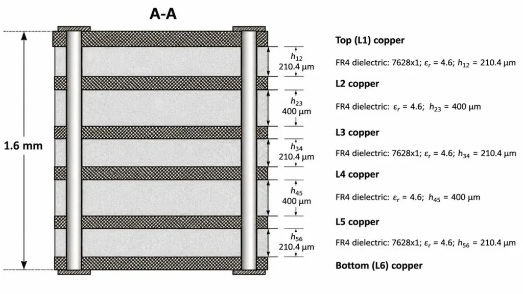
Router PCB Materials and Multilayer Stackup with FR-4 and Low-Loss Dielectric Layers
The right router PCB material and stackup depend on operating frequency, signal-loss limits, board thickness, routing density, thermal requirements, manufacturing capability, and cost targets. Standard FR-4 is often suitable for conventional digital and many wireless router designs, while low-loss laminates may be appropriate for demanding RF or high-speed signal paths.
When Is Standard FR-4 Suitable for a Router PCB?
FR-4 is a common choice because it offers a practical balance of cost, mechanical strength, electrical properties, and manufacturing availability.
It may be appropriate when the design’s RF and digital performance requirements can be met with the selected material’s dielectric properties and loss characteristics.
Before approving FR-4, buyers should confirm:
- The required dielectric constant and loss tangent at relevant frequencies.
- The target impedance and associated manufacturing tolerances.
- The finished board thickness and copper configuration.
- The thermal and reliability requirements.
- The availability and consistency of the specified laminate.
FR-4 is a material family rather than one universal electrical specification. Different grades can have substantially different properties.
When Should Buyers Consider Low-Loss High-Frequency Laminates?
Low-loss materials may be useful when RF insertion loss, dielectric stability, or high-frequency signal performance becomes a limiting factor.
Material selection should consider the entire signal path, including connectors, copper roughness, transmission-line geometry, and transitions between different materials.
| Selection factor | What buyers should evaluate |
|---|---|
| Dielectric constant (Dk) | Impedance calculations, propagation characteristics, and design consistency |
| Dissipation factor (Df) | Dielectric losses at the relevant operating frequency |
| Copper roughness | Conductor loss, particularly on higher-frequency signal paths |
| Thermal expansion | Reliability during fabrication, soldering, and operating-temperature changes |
| Material availability | Approved grades, lead times, and production continuity |
| Total cost | Laminate price, processing complexity, yield risk, and volume requirements |
Do not specify an expensive high-frequency laminate simply because the product supports a modern wireless standard. Request an engineering review to determine whether the expected electrical benefit justifies the additional material and processing cost.
How Should Layer Count, Copper Weight, and Board Thickness Be Selected?
Layer count should follow routing density, signal-integrity requirements, ground-plane continuity, power distribution, and mechanical constraints.
A two-layer board may be sufficient for a simple design. More complex routers may require multilayer construction to accommodate dense routing, high-speed interfaces, power planes, and RF isolation.
The stackup should be reviewed as a complete electrical and manufacturing structure.
Key inputs include:
- Number and arrangement of signal, ground, and power layers.
- Finished board thickness and dielectric spacing.
- Copper thickness on internal and external layers.
- Controlled-impedance requirements.
- Via structures and drilling limitations.
- Component clearances and mechanical dimensions.
For projects requiring tighter routing or higher interconnect density, buyers can also review the relevant HDI PCB manufacturing capabilities. The actual suitability of HDI should be determined by the design’s routing and interconnection requirements.
How Does Router PCB Design Affect RF Performance and EMI?
Router PCB design directly affects RF losses, signal integrity, electromagnetic compatibility, and thermal behavior. Manufacturers should review fabrication constraints alongside the design team’s electrical requirements before production begins.
How Should RF and Digital Circuits Be Partitioned?
RF circuits and high-speed digital circuits can interfere with each other through shared return paths, parasitic coupling, supply noise, and poorly controlled transitions.
Good layout practices include:
- Positioning RF components to minimize unnecessary interconnect length.
- Maintaining suitable transmission-line geometry.
- Preserving reference-plane continuity.
- Controlling coupling between sensitive RF paths and noisy digital or switching-power circuits.
- Following component manufacturers’ recommended layouts where applicable.
- Reviewing connectors, launches, vias, and other discontinuities.
Circuit partitioning should reflect the actual signal paths and current-return behavior. Arbitrarily dividing the PCB into isolated zones without considering grounding and return paths can introduce new problems.
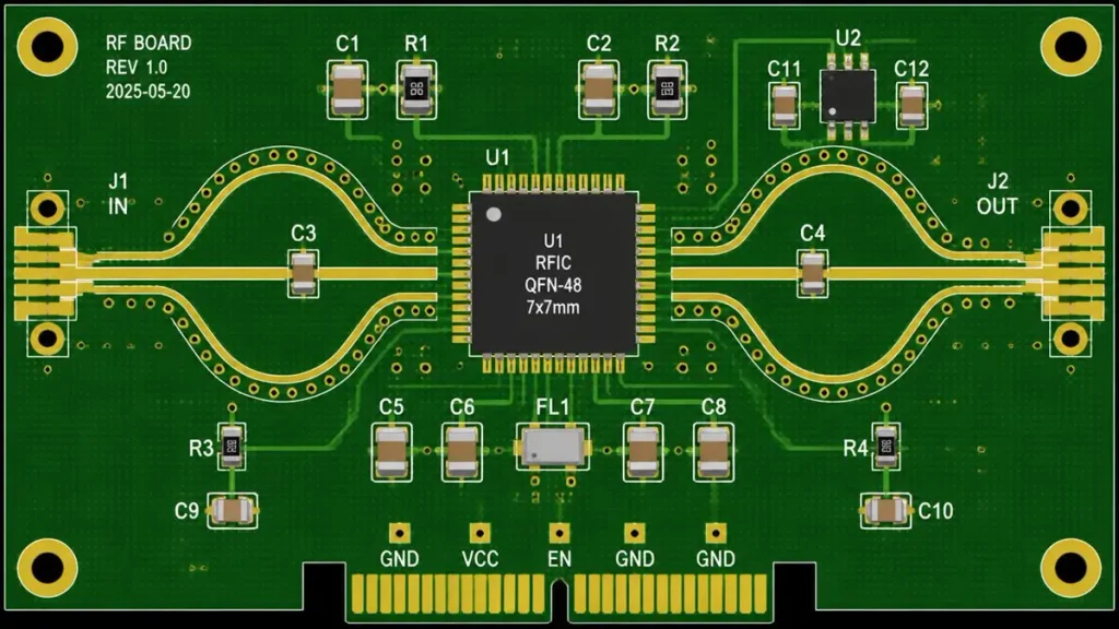
Router PCB RF Design Showing Antenna Feed Lines, Ground Planes, Shielding, and EMI Control
How Do Ground Planes and Return Paths Affect Signal Integrity?
A continuous reference plane provides a predictable return path for many high-speed and RF signals. Splits, voids, inappropriate plane transitions, and poorly positioned stitching vias can increase loop inductance and create unwanted coupling.
During design review, check whether critical signals maintain an appropriate reference plane throughout their routes. Where a signal transitions between reference planes or layers, the return-current path must also be considered.
For controlled-impedance signals, the finished geometry depends on copper width and thickness, dielectric height, material properties, and the surrounding reference structure. The manufacturer should review the stackup and identify any constraints before fabrication.
For designs with demanding digital interconnects, PCBKR’s high-speed PCB manufacturing information provides a related starting point for evaluating manufacturing requirements.
How Can Antenna Clearance and RF Feed Routing Be Preserved?
Antenna performance depends on more than the PCB feed line. Antenna geometry, the ground structure, enclosure materials, nearby components, cables, and installation conditions can all affect matching and radiation characteristics.
The design review should verify:
- The antenna manufacturer’s recommended clearance and ground requirements.
- RF feed geometry and impedance.
- The placement of matching components.
- The effect of nearby metal, connectors, batteries, and heat sinks.
- The accessibility of test points and RF connectors, where required.
- Whether antenna tuning and over-the-air testing are included in the validation plan.
PCB fabrication inspection cannot by itself establish the final antenna efficiency or wireless range. Those properties require suitable RF measurements and, where necessary, system-level testing.
How Should Power Integrity and Thermal Management Be Addressed?
Networking processors, radio-frequency power amplifiers, and voltage regulators can create localized heat and transient current demands.
The design should account for power-distribution impedance, decoupling, copper-plane capacity, thermal paths, component placement, and enclosure airflow.
For procurement, it is important to distinguish between the manufacturer’s ability to fabricate the specified copper structure and the engineering team’s responsibility for validating system-level thermal performance.
How Are Router PCBs Manufactured and Assembled?
Router PCB production generally involves engineering review, bare-board fabrication, inspection, component assembly where required, and final verification. The exact process depends on the layer count, materials, via structures, assembly complexity, and acceptance criteria.
What Happens During Multilayer Router PCB Fabrication?
A typical multilayer PCB fabrication process includes:
- Engineering review: Check design files, stackup, drill data, tolerances, and manufacturing constraints.
- Inner-layer imaging: Transfer the circuit pattern onto the specified copper layers.
- Etching and inspection: Form and inspect the inner-layer circuitry.
- Lamination: Bond the multilayer structure under controlled process conditions.
- Drilling and via formation: Create the required holes and interlayer connections.
- Copper plating: Establish conductive connections through plated holes and vias.
- Outer-layer patterning: Form the external circuit patterns.
- Solder mask and surface finish: Apply the specified protective coating and finish.
- Electrical and dimensional inspection: Verify the applicable acceptance requirements.
- Final review and shipment: Confirm the finished boards meet the approved specification.
The precise process sequence can vary by board construction. Buyers should confirm that the selected supplier can manufacture the required stackup, via structures, tolerances, and material combination.
How Are RF Components, BGAs, and Fine-Pitch Devices Assembled?
Router PCBA assembly may include surface-mount components, fine-pitch ICs, BGAs, connectors, shields, and through-hole parts.
The assembly process typically includes solder-paste printing, component placement, reflow soldering, inspection, and any required through-hole or secondary operations.
The assembly plan should consider:
- Component package types and pitches.
- Approved component alternatives.
- Moisture-sensitive device handling.
- Soldering profiles and thermal limitations.
- RF shielding and connector installation.
- Inspection accessibility and test-point design.
A supplier’s SMT capability should be assessed against the actual component packages and assembly requirements rather than a general claim of advanced assembly capability.
What Changes Between Prototype, NPI, and Mass Production?
Prototype production is primarily used to verify design assumptions and identify issues before a larger commitment. New product introduction (NPI) adds process validation and production readiness, while mass production requires repeatability, traceability, and stable supply-chain management.
| Production stage | Main objective | Recommended buyer checks |
|---|---|---|
| Prototype | Verify initial design and manufacturing feasibility | Dimensions, connectivity, assembly quality, initial functional tests |
| NPI or pilot build | Identify process and design risks | DFM closure, assembly yield, test coverage, approved changes |
| Mass production | Maintain consistent output | Process controls, traceability, defect monitoring, change management |
A successful prototype does not automatically guarantee mass-production performance. Buyers should define acceptance criteria and review unresolved issues before approving volume production.
Which Quality Tests Should Buyers Require for Router PCBA?
Router PCBA quality assurance should combine inspection, electrical verification, and functional testing appropriate to the design. RF performance testing must be specified separately when the product’s requirements extend beyond visual and basic electrical inspection.
Which Manufacturing Inspections Are Appropriate?
| Test or inspection | Primary purpose | Important limitation |
|---|---|---|
| Automated optical inspection (AOI) | Detect visible assembly defects and component-placement issues | Cannot verify all hidden solder joints or RF performance |
| X-ray inspection | Examine hidden joints such as many BGA connections | Does not establish complete functional reliability |
| In-circuit testing (ICT) | Check accessible electrical characteristics and assembly faults | Depends on test access, coverage, and fixture strategy |
| Flying-probe testing | Perform electrical checks without a dedicated ICT fixture | Coverage and throughput depend on the board and test program |
| Bare-board electrical testing | Check applicable opens and shorts in fabricated PCB circuitry | Does not validate the assembled router’s operation |
| Functional testing | Verify defined board-level functions using an appropriate test setup | Only verifies the functions and conditions included in the test |
The required inspection plan should be agreed upon before quotation. Test selection depends on package types, design-for-test provisions, volume, failure risks, and customer acceptance requirements.
How Should RF Performance and Antenna Matching Be Validated?
RF validation should use equipment and test methods appropriate to the operating frequencies and the required performance metrics.
Depending on the product, the test plan may include:
- RF path measurements, such as insertion loss and return loss.
- Antenna matching or S-parameter measurements.
- Verification of relevant transmit and receive characteristics.
- Functional checks of Ethernet, wireless interfaces, and power circuits.
- Shielding or EMC testing where required by the product specification.
- Over-the-air or system-level testing where the acceptance criteria require it.
A network analyzer, spectrum analyzer, or other RF test equipment may be necessary depending on the measurement. The instrument, calibration, fixtures, test limits, and reporting format should match the actual requirement.
A board-level functional test is not a substitute for a complete RF or regulatory compliance test.
Which Quality Documents Should Buyers Request?
Before production, agree on which records are required for each batch. Depending on the project, the documentation package may include:
- Approved stackup and fabrication drawing.
- Material and surface-finish specifications.
- Bare-board electrical test results.
- Impedance test reports, where controlled impedance is specified.
- Assembly inspection records.
- Component traceability and approved substitution records.
- Functional and RF test results, where included in the scope.
- Nonconformance reports and corrective-action records.
For projects requiring formal quality systems or industry-specific certifications, buyers should verify the supplier’s actual certificate scope and validity. Certifications should never be assumed solely because a supplier manufactures electronics.
How Can Buyers Select a Reliable Router PCB Manufacturer?
A reliable router PCB manufacturer should demonstrate that it can meet the project’s technical specification, maintain consistent manufacturing quality, communicate engineering risks, and support the required production volume.
Which Manufacturing Capabilities Should Be Verified?
Evaluate the supplier against the actual requirements rather than relying on a general capability statement.
| Evaluation area | Questions to ask the supplier |
|---|---|
| PCB fabrication | Can the factory manufacture the specified layers, thickness, copper weights, and via structures? |
| Material control | Can the specified laminate grade be sourced and controlled consistently? |
| Impedance control | Can the supplier review the stackup and provide the agreed test evidence? |
| Assembly | Can the process support the required BGA, fine-pitch, RF, and connector packages? |
| Quality testing | Which inspections and electrical or functional tests are available in-house? |
| Traceability | Can material lots, production batches, and relevant test results be linked? |
| Engineering support | Can DFM issues and proposed substitutions be reviewed before production? |
| Production scaling | Can the supplier support the planned transition from prototype to volume? |
Request specific evidence for critical capabilities, such as representative inspection records, approved process documentation, and relevant test reports. A supplier should be able to explain both what it can do and where additional validation or an external testing partner may be required.
How Should Buyers Compare Prototype and Mass-Production Quotes?
The lowest unit price may not represent the lowest total project cost.
A meaningful comparison should include the same board specification, materials, quantities, assembly scope, component assumptions, test coverage, and delivery requirements.
Check whether each quotation includes:
- Engineering review and tooling or fixture charges.
- PCB fabrication and surface finish.
- Component procurement and approved substitutions.
- SMT and through-hole assembly.
- Inspection and functional testing.
- Packaging, shipping, and any agreed documentation.
- Potential nonrecurring engineering costs and production-change charges.
Ask suppliers to identify exclusions explicitly. Differences in scope are a common reason apparently similar quotations are not directly comparable.
What Should Buyers Ask Before Supplier Approval?
Before selecting a manufacturer, ask:
- Can you manufacture the specified PCB stackup and material combination?
- Which design constraints could affect cost, yield, or lead time?
- How will impedance requirements be reviewed and verified?
- Which inspections and tests are included in the quotation?
- How are component substitutions approved and recorded?
- What information will be provided for batch traceability?
- How are engineering changes controlled between prototype and production?
- What is the process for handling nonconforming boards or assemblies?
Clear answers help buyers distinguish a technically suitable manufacturing partner from a supplier that can only provide a generic price.
How Much Does Router PCB Manufacturing Cost?
Router PCB manufacturing cost depends on the board design, material, production quantity, fabrication complexity, assembly requirements, component sourcing, testing, and delivery schedule. There is no reliable universal price for a router PCB without a defined specification and quantity.
How Do PCB Specifications Affect Cost?
| Cost driver | Why it matters | How buyers can optimize it |
|---|---|---|
| Layer count | More layers generally increase fabrication complexity | Use the minimum stackup that meets electrical and routing requirements |
| Material | Specialized laminates may cost more and require specific processes | Select material based on validated electrical needs |
| Board dimensions | Larger panels and different utilization affect material consumption | Review panelization and board dimensions |
| Via structures | More complex interconnections can add process steps | Avoid unnecessary complexity while preserving reliability |
| Impedance requirements | Require design review and may require additional testing | Define targets and tolerances clearly |
| Surface finish | Different finishes have different costs and suitability | Select according to component and reliability requirements |
| Production quantity | Setup costs and panel utilization affect unit economics | Compare prototype, pilot, and volume pricing |
| Assembly complexity | Component packages and placement density affect labor and process needs | Optimize for manufacturability without compromising function |
| Testing | Additional fixtures, test programs, and RF validation add cost | Define risk-based test coverage before production |
How Can Buyers Reduce Cost Without Increasing Reliability Risks?
Cost reduction should focus on unnecessary complexity, poor procurement planning, and avoidable rework—not indiscriminate reductions in material quality or inspection.
Useful actions include:
- Completing DFM and DFA reviews before ordering prototypes.
- Standardizing materials and finishes where technically appropriate.
- Avoiding unnecessary layer count or complex via structures.
- Freezing the BOM and controlling approved alternatives.
- Designing test access into the board.
- Comparing quotations against an identical scope of supply.
- Resolving prototype issues before committing to volume.
A modest design change can sometimes reduce fabrication or assembly complexity substantially, but its impact should be assessed by engineering and validated against the product requirements.
What Information Is Needed for a Router PCB Manufacturing Quote?
A complete RFQ helps the supplier estimate cost, feasibility, and lead time more accurately. Missing design files, unclear test requirements, or undefined component alternatives often create avoidable delays during quotation and engineering review.
Which Files Should Buyers Submit?
For bare PCB fabrication:
- Gerber files or ODB++ data.
- Drill files and fabrication drawing.
- Layer count and proposed stackup.
- Board dimensions and finished thickness.
- Copper weights and surface finish.
- Impedance targets and tolerances, where applicable.
- Quantity and required delivery date.
- Applicable acceptance standards and inspection requirements.
For PCBA assembly:
- Complete BOM with manufacturer part numbers.
- Pick-and-place or centroid files.
- Assembly drawings and polarity information.
- Approved component alternatives.
- PCB fabrication data.
- Required assembly processes and inspection criteria.
- Functional test specifications and fixtures, where applicable.
- Prototype, pilot, and mass-production quantities.
For RF-intensive router projects:
- RF performance requirements and applicable frequency bands.
- Controlled-impedance specifications.
- Antenna and connector interface requirements.
- RF measurement or functional test limits.
- Shielding and enclosure constraints, where relevant.
Not every project requires every item. The goal is to supply enough information for a meaningful engineering and commercial review.
How Can Buyers Avoid Quotation Delays?
Before submission, ensure that all files refer to the same revision. Confirm whether components will be supplied by the customer or sourced by the manufacturer, and state whether testing, programming, shielding, or enclosure integration is included.
If the design is still under development, identify open issues rather than presenting provisional specifications as final requirements. The supplier can then distinguish confirmed costs from assumptions requiring engineering review.
Request a Router PCB Manufacturing Quote
Shenzhen Hongda Circuit Technology Co., Ltd. supports PCB fabrication and PCBA manufacturing inquiries for customers evaluating prototype, pilot-production, and mass-production requirements.
To discuss your project, provide the available design files, PCB specifications, BOM, production quantity, and required testing scope.
- Website: https://www.pcbkr.com/
- Email: pcb@pcbkr.com
Submit the requirements for an engineering review so that manufacturing constraints, quotation assumptions, and production needs can be discussed before the order is placed.
Frequently Asked Questions About Router PCB Manufacturing
What Is a Router PCB?
A router PCB is the printed circuit board used to connect the processing, networking, wireless, power, and interface components in a router. Its design and manufacturing quality influence electrical performance, assembly reliability, and the ability to meet the product’s operating requirements.
How Many Layers Does a Wi-Fi Router PCB Need?
The required layer count depends on component density, routing complexity, RF requirements, grounding, power distribution, and mechanical constraints. Simple designs may use two layers, while more complex routers may need multilayer construction. The final stackup should be determined through electrical design and manufacturing review.
Which Materials Are Suitable for a Router PCB?
FR-4 is suitable for many router designs, provided its electrical and thermal properties meet the requirements. Low-loss laminates may be appropriate for demanding RF or high-speed signal paths. Buyers should compare dielectric properties, copper roughness, material availability, processing requirements, and total cost.
How Can EMI Be Reduced in a Router PCB?
EMI can be reduced through appropriate circuit partitioning, continuous reference planes, controlled return paths, suitable decoupling, careful RF routing, and effective shielding where required. The final design should be validated through relevant electrical, EMC, and system-level tests.
What Is the Difference Between Router PCB Fabrication and Router PCBA Assembly?
PCB fabrication produces the bare circuit board. PCBA assembly mounts electronic components onto the board using processes such as SMT and through-hole soldering. A turnkey service may combine fabrication, component sourcing, assembly, and agreed testing.
How Much Does Custom Router PCB Manufacturing Cost?
Cost depends on the board dimensions, layer count, materials, via structures, quantity, assembly complexity, component sourcing, and test requirements. A comparable quotation requires a defined specification and production scope. Buyers should compare total project cost rather than unit price alone.
What Tests Should Be Required for Router PCBA?
Typical requirements may include AOI, X-ray inspection for applicable hidden joints, electrical testing, and functional testing. RF-intensive designs may also require impedance verification, RF path measurements, antenna matching, or system-level validation. The test plan should match the actual acceptance criteria.
How Do I Choose a Reliable Router PCB Manufacturer?
Evaluate the manufacturer’s ability to meet the required stackup, material, impedance, assembly, inspection, and traceability requirements. Request relevant process evidence and test records, clarify exclusions in the quotation, and establish a controlled transition from prototype to mass production.
What Files Are Required for a Router PCB Quote?
Bare-board quotations typically require Gerber or ODB++ data, drill files, a fabrication drawing, stackup requirements, quantities, and acceptance criteria. PCBA quotations also require a BOM, placement data, assembly drawings, component sourcing instructions, and the required testing scope.
How Long Does Router PCB Production Take?
Lead time depends on board complexity, material availability, fabrication requirements, component sourcing, assembly, testing, and production capacity. Prototype and mass-production schedules should be quoted separately after reviewing the project specification. Buyers should also confirm whether the quoted schedule includes component procurement and functional testing.
Conclusion: How Can Buyers Source the Right Router PCB Manufacturing Partner?
Successful router PCB procurement requires alignment between electrical design, material selection, manufacturing capability, assembly quality, and validation requirements. A suitable supplier should understand the difference between bare-board fabrication and complete PCBA delivery, identify manufacturing risks early, and provide evidence that the agreed specifications can be met consistently.
For OEMs and engineering teams, the most effective approach is to define the required performance, prepare a complete RFQ package, compare suppliers against the same technical scope, and resolve prototype issues before volume production.
Contact Shenzhen Hongda Circuit Technology Co., Ltd. at pcb@pcbkr.com or visit https://www.pcbkr.com/ to discuss your router PCB fabrication and PCBA manufacturing requirements.
About Author
David Chen LinkedIn Profile
David Chen is a Senior RF/PCB Process Engineer at Shenzhen Hongda Circuit Technology Co., Ltd., with over 12 years of experience in high-frequency PCB fabrication, impedance-controlled stack-up design, and Rogers/PTFE laminate processing. He also boasts an extensive professional background in PCBA manufacturing, PCBA testing, and PCBA optimization, with specialized expertise in high-precision PCBA fault analysis and rigorous PCBA reliability testing. The author has worked with high-layer-count server PCB fabrication, ultra-low-loss backplane stackups, and thermo-mechanical reliability optimization for AI infrastructure projects involving 112G and 224G PAM4 architectures. Skilled in complex circuit design and cutting-edge advanced PCB manufacturing processes, he delivers solutions that elevate product durability and performance across industrial applications. His technical articles focusing on PCBA manufacturing workflows and testing methodologies are widely cited by industry peers and technical platforms, and have gained attention and recognition from industry colleagues.