How Do You Choose a Tactile Sensor PCB Manufacturer for Robotics OEM Projects?
A reliable tactile sensor PCB manufacturer must deliver more than a circuit board: the design must support sensor-array integration, low-noise signal acquisition, mechanical constraints, and repeatable production. Robotics OEM buyers should evaluate PCB structure, fine-line fabrication, assembly quality, electrical testing, and the supplier’s ability to support prototypes through volume production.
For robotic grippers, collaborative robots, and force-feedback systems, the right manufacturing partner helps reduce interconnection risks and makes the transition from engineering prototypes to production more predictable.
What Does a Tactile Sensor PCB Manufacturer Need to Deliver?
A tactile sensor PCB connects sensing elements with the electronics that acquire, condition, process, and transmit sensor signals. Depending on the design, the assembly may include resistive or capacitive sensing elements, strain gauges, analog front ends, amplifiers, ADCs, microcontrollers, and communication interfaces.
The PCB manufacturer must understand how these elements affect layout, interconnection, assembly, and test requirements.
| Buyer requirement | Manufacturing consideration | What to confirm with the supplier |
|---|---|---|
| Sensor-array integration | Pad geometry, routing density, and interconnection | Can the fabrication process meet the supplied design rules? |
| Low-level signal acquisition | Grounding, return paths, and separation of sensitive signals | Can engineering review the layout and stack-up? |
| Compact robotic hardware | Board outline, connector placement, and component clearance | Can the PCB fit the mechanical envelope? |
| Flexible sensor placement | Bend zones, copper geometry, and material selection | Is a flex or rigid-flex structure appropriate? |
| Repeatable production | Process control and inspection coverage | Which inspection and electrical tests are included? |
| Production scalability | Panelization, assembly yield, and component availability | Can the supplier support the planned production stages? |
The appropriate solution depends on the sensing technology, mechanical arrangement, signal-conditioning circuit, and operating environment. A PCB supplier should assess these requirements before recommending a stack-up or manufacturing process.
Which PCB Structure Is Best for a Robotic Tactile Sensor?
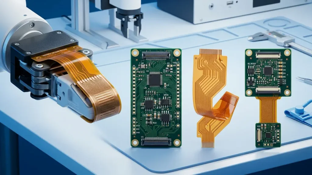
Rigid, flex, and rigid-flex PCB structures for compact robotic tactile sensing and force-feedback applications.
The best structure depends on sensor placement, available space, interconnection density, and whether the circuit must bend during operation.
Rigid PCBs are often suitable for fixed sensor-interface electronics, ADCs, microcontrollers, and communication circuits. Multilayer construction may help separate analog and digital routing or provide more controlled reference planes when the design requires them.
For compact sensor arrays with dense routing requirements, HDI PCB manufacturing may be worth evaluating. High-density interconnection can help accommodate fine-pitch components and complex routing within a limited footprint, subject to the actual design rules and cost target.
When the sensing elements are distributed across a curved surface or moving part, a Flex PCB solution may simplify the interconnection between the sensing area and the main electronics. The designer must specify whether the flex section is static or dynamically bent, together with its bend radius, expected movement, and service life.
For robotic grippers or joints that need rigid component-mounting areas connected through flexible sections, Rigid-Flex PCB manufacturing can be considered. Integrating rigid and flexible sections may reduce separate cable connections, but the design must account for bend zones, layer transitions, stiffeners, and assembly constraints.
The choice should be driven by mechanical and electrical requirements—not by selecting the most complex PCB structure available.
How Can PCB Manufacturing Affect Tactile Sensor Signal Quality?
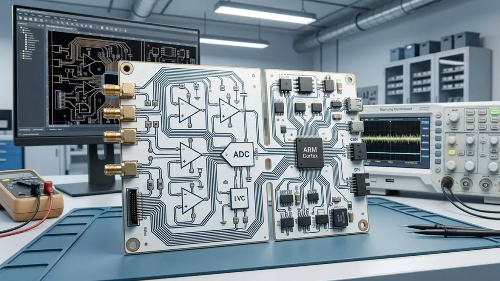
PCB layout, grounding, and signal routing influence noise coupling and signal integrity in robotic tactile sensor systems
Tactile sensing performance depends on the complete measurement chain, including the sensor element, analog front end, PCB layout, power supply, grounding, firmware, and calibration process. PCB fabrication alone cannot guarantee sensor accuracy, but manufacturing defects or unsuitable layout decisions can compromise signal quality.
Four areas deserve particular attention.
1. Routing and grounding
Low-level analog signals should be routed with suitable reference paths and separation from noisy switching or digital circuits. Grounding and shielding must follow the circuit architecture; indiscriminate copper fills or ground connections can sometimes introduce unwanted coupling.
2. Fine-line accuracy and registration
Dense sensor arrays and fine-pitch components may require precise trace geometry, pad definition, and layer registration. PCBKR’s manufacturing processes include laser direct imaging (LDI) and modified semi-additive processing (mSAP) for applicable fine-line designs. The achievable result must be confirmed against the specific stack-up, copper thickness, line/space requirements, and production conditions.
3. Via and interlayer reliability
Multilayer sensor interfaces may contain small vias and dense interconnections. The selected drilling process, aspect ratio, layer alignment, plating requirements, and finished-board inspection plan should be reviewed against the actual design.
4. Power and data interfaces
If the sensor electronics use a high-speed data interface, the designer should assess impedance, routing topology, return paths, and crosstalk. For projects with explicit high-speed transmission requirements, review High-Speed PCB manufacturing as a related capability.
A high-frequency board is not automatically necessary for a tactile sensor. Consider High-Frequency PCB solutions only when the design includes a genuine RF or microwave signal requirement. For many tactile sensing systems, noise control and measurement stability are more important than RF-specific materials.
Finally, distinguish PCB electrical continuity from sensor performance validation. A flying-probe or other electrical test can detect specified open circuits and shorts, but it does not independently verify sensor sensitivity, linearity, hysteresis, drift, or force calibration. Those characteristics require appropriate sensor-level or system-level testing.
What Should Buyers Check Before Approving a Tactile Sensor PCB Design?
Before releasing the design for fabrication, buyers should confirm that the manufacturing package is complete and internally consistent.
- Fabrication data: Gerber or other agreed production data, drill files, board outline, copper thickness, finish, and fabrication notes.
- Stack-up: Layer count, material, finished thickness, copper distribution, and impedance requirements where applicable.
- Mechanical integration: Mounting holes, sensor contact areas, connector locations, stiffeners, bend zones, and enclosure clearances.
- Assembly documentation: BOM, component designators, placement files, polarity information, and assembly drawings.
- Test requirements: Defined continuity, isolation, functional, or other acceptance criteria.
- Revision control: Matching revision numbers across fabrication files, BOM, assembly drawings, and test documentation.
For a flex or rigid-flex design, buyers should also provide the bending conditions, bend radius, expected cycle count, and restrictions on component placement within flexible regions.
A design-for-manufacturing (DFM) review should identify problems before production, rather than relying on inspection to catch every issue after fabrication. Ask the supplier to clarify any manufacturability concern and document the agreed design changes before approving the production files.
Which PCB Assembly and Testing Processes Are Needed for Tactile Sensors?

PCB fabrication, automated inspection, X-ray inspection, and electrical testing help verify manufacturing quality before tactile sensor system validation.
The required process depends on whether the project involves bare PCB fabrication, PCBA, or a complete sensor module.
For an assembled sensor-interface board, the process may include SMT placement, solder-paste printing, reflow soldering, inspection, and electrical or functional testing. Through-hole assembly may be required for selected connectors or mechanical components.
The inspection plan should be matched to the product risks:
| Process or test | What it helps verify | Important limitation |
|---|---|---|
| Automated optical inspection (AOI) | Visible soldering and assembly defects, according to inspection coverage | Does not measure tactile sensitivity |
| X-ray inspection | Hidden solder joints, such as selected BGA connections | Applicability depends on package type and acceptance criteria |
| Flying-probe or fixture-based electrical testing | Defined opens, shorts, and electrical connections | Does not replace functional sensor calibration |
| Functional testing | Operation against a defined electrical or system test procedure | Requires agreed test fixtures, limits, and test instructions |
| Sensor calibration | Output response against known force or stimulus points | Requires suitable sensor-level equipment and a calibration method |
For projects combining sensor interfaces, processors, and dense interconnections, buyers may evaluate PCBKR’s HDI PCB manufacturing capabilities alongside the assembly and test requirements.
Before ordering, confirm which tests are included in the quotation, which fixtures or test programs the buyer must provide, and whether calibration is included or handled by the OEM. These distinctions help avoid gaps between PCB delivery and final product acceptance.
How Can Buyers Move from Tactile Sensor PCB Prototypes to Production?
A staged process helps robotics OEMs identify manufacturing risks early and avoid unnecessary redesigns.
Stage 1: Engineering review
Provide the PCB data, BOM, mechanical constraints, sensor technology, and target production quantity. Review stack-up, manufacturability, component availability, and test coverage.
Stage 2: Prototype fabrication and assembly
Build a representative prototype using the intended materials and assembly process where practical. Check mechanical fit, connector access, sensor integration, and electrical operation.
Stage 3: Design verification
Evaluate the complete sensing system against defined requirements. Depending on the application, this may include repeatability, linearity, hysteresis, drift, temperature response, and mechanical-cycle testing.
Stage 4: Pilot production
Confirm the production files, inspection criteria, test procedures, and change-control process. Review any assembly or fabrication issues identified during the prototype stage.
Stage 5: Volume production
Use an approved revision and agreed acceptance criteria. Monitor relevant yield and defect data, and ensure that engineering changes are reviewed before implementation.
A manufacturer can support fabrication and assembly, but the OEM should define the required sensor performance and system acceptance tests. Assigning these responsibilities clearly helps avoid disputes over what constitutes a conforming product.
What Determines the Cost and Lead Time of a Custom Tactile Sensor PCB?
PCB cost and lead time depend on more than board dimensions. The principal factors include:
- Layer count, board size, and panel utilization.
- Minimum line/space, via dimensions, and interconnection complexity.
- Rigid, flex, or rigid-flex construction and material selection.
- Copper thickness, surface finish, and special fabrication requirements.
- Component count, package types, BOM availability, and assembly complexity.
- Inspection coverage, test fixtures, and required documentation.
- Prototype quantity, production volume, and delivery schedule.
A compact rigid sensor-interface PCB may be relatively straightforward, while a flexible sensor array with fine-pitch assembly and specialized validation may require more engineering work.
To obtain a meaningful quotation, buyers should provide the target quantity and delivery date alongside the technical files. If the design is still under development, state which specifications are fixed and which can be optimized. This allows the supplier to identify cost-saving options without compromising critical electrical or mechanical requirements.
What Should Be Included in a Tactile Sensor PCB RFQ?
A complete request for quotation (RFQ) should give the manufacturer enough information to evaluate fabrication, assembly, inspection, and delivery requirements.
Use this checklist before submitting your inquiry:
- Gerber files or other agreed fabrication data.
- Drill files, board outline, and mechanical drawings.
- Stack-up, layer count, material, copper thickness, and surface finish.
- BOM with manufacturer part numbers and approved alternatives, if any.
- Pick-and-place files and assembly drawings for PCBA.
- Sensor type and relevant interface requirements.
- Mechanical constraints, including bend radius and expected flex cycles where applicable.
- Required electrical tests, functional tests, and acceptance criteria.
- Prototype and production quantities.
- Target delivery date and shipping destination.
- Required quality records, traceability, or other project-specific documentation.
If calibration or force-response verification is required, include the expected measurement range, acceptance limits, and test method. Do not assume that these services are included in a standard PCB or PCBA quotation.
A clear RFQ allows the supplier to identify missing information, propose feasible manufacturing options, and quote against a defined scope.
How Can Robotics OEMs Evaluate PCBKR for a Tactile Sensor PCB Project?
When evaluating PCBKR as a manufacturing partner, robotics OEMs should match the project requirements to the relevant fabrication and assembly processes rather than rely on general capability statements.
Shenzhen Hongda Circuit Technology Co., Ltd. supports PCB manufacturing and PCBA projects, including fine-line fabrication and inspection processes. Depending on the design, the engineering review may consider LDI pattern imaging, mSAP processing, laser drilling, multilayer lamination, AOI, X-ray inspection, and electrical testing.
For robotic grippers, collaborative robots, and compact sensor interfaces, buyers can compare the design requirements with PCBKR’s Collaborative Robot PCB manufacturing offering. If the sensor requires flexible interconnection, high-density routing, or high-speed data transmission, the related product pages linked above can help buyers assess the appropriate technology path.
To speed up technical evaluation, submit the fabrication files, BOM, quantity, target lead time, and test requirements together. The quotation should clarify the proposed construction, included inspection and testing, assumptions, and any unresolved engineering questions.
Contact Shenzhen Hongda Circuit Technology Co., Ltd. at sales@pcbkr.com or visit www.pcbkr.com to discuss a custom tactile sensor PCB or PCBA project.
Frequently Asked Questions About Tactile Sensor PCB Manufacturing
Which PCB type is best for a robotic tactile sensor?
A rigid PCB is often suitable for fixed sensor-interface electronics. Flex PCB may suit curved or moving sensing areas, while rigid-flex PCB can combine rigid component-mounting zones with flexible interconnections. The final choice depends on the sensor arrangement, mechanical movement, and routing requirements.
Can HDI PCB manufacturing help reduce the size of a tactile sensor board?
HDI manufacturing can support dense routing and fine-pitch components in compact designs. Whether it is the best option depends on the required line/space, via structure, stack-up, reliability targets, and budget.
Does PCB electrical testing verify tactile sensor accuracy?
No. Standard electrical tests can verify specified interconnections and detect certain manufacturing defects, but they do not independently establish force sensitivity, linearity, hysteresis, or calibration accuracy. These require defined sensor-level or system-level tests.
What files are needed for a tactile sensor PCB quotation?
Typically, provide fabrication data, drill files, stack-up details, mechanical drawings, BOM, assembly files if PCBA is required, order quantities, target lead time, and test requirements. Include bend and calibration specifications when relevant.
Can a PCB manufacturer support both prototypes and mass production?
A manufacturer may support multiple production stages, but buyers should confirm the available processes, engineering review, assembly scope, quality controls, lead times, and production-volume requirements for their particular design. Prototype approval should include a clear plan for transferring the validated design into production.
RFQ Contact Tactile Sensor PCB Manufacturer
Shenzhen Hongda Circuit Technology Co., Ltd.
Email: sales@pcbkr.com
Website: www.pcbkr.com
About Author
David Chen LinkedIn Profile
David Chen is a Senior RF/PCB Process Engineer at Shenzhen Hongda Circuit Technology Co., Ltd., with over 12 years of experience in high-frequency PCB fabrication, impedance-controlled stack-up design, and Rogers/PTFE laminate processing. He also boasts an extensive professional background in PCBA manufacturing, PCBA testing, and PCBA optimization, with specialized expertise in high-precision PCBA fault analysis and rigorous PCBA reliability testing. The author has worked with high-layer-count server PCB fabrication, ultra-low-loss backplane stackups, and thermo-mechanical reliability optimization for AI infrastructure projects involving 112G and 224G PAM4 architectures. Skilled in complex circuit design and cutting-edge advanced PCB manufacturing processes, he delivers solutions that elevate product durability and performance across industrial applications. His technical articles focusing on PCBA manufacturing workflows and testing methodologies are widely cited by industry peers and technical platforms, and have gained attention and recognition from industry colleagues.