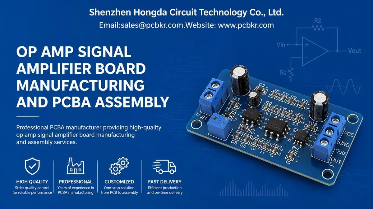
Op-Amp Signal Amplifier Board Manufacturing and PCBA Assembly
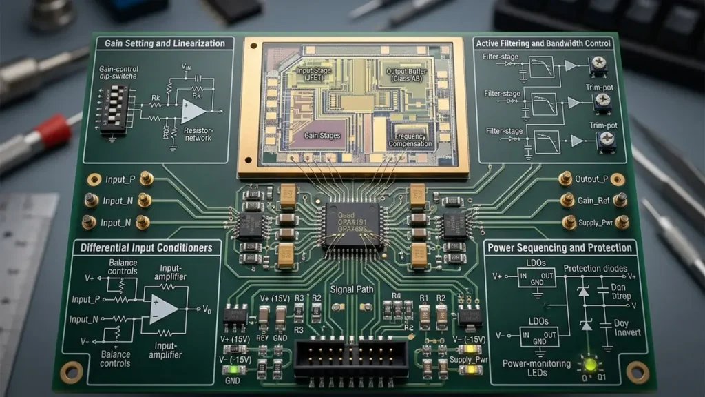
PCB Material: FR-4 / High-Tg FR-4 / Low-Noise Circuit-Compatible PCB Materials
Layers: 2–8 Layers (design-dependent)
Board Thickness: According to PCB design and stackup requirements
Minimum Trace Width / Spacing: According to circuit layout and manufacturing requirements
Minimum Hole Size: According to PCB design, via structure and manufacturing requirements
An Op-Amp Signal Amplifier Board is designed to amplify, condition, buffer, or convert low-level analog signals for measurement, sensing, industrial control, and data acquisition applications. Reliable performance depends on more than the operational amplifier IC. Feedback routing, grounding, power supply decoupling, PCB material selection, surface cleanliness, thermal behavior, and assembly consistency all influence the final circuit. Shenzhen Hongda Circuit Technology Co., Ltd. provides custom PCB fabrication and PCBA assembly for OEM customers developing precision analog and signal-conditioning products, from prototypes to production orders.
1. Op-Amp Signal Amplifier Board Functions and Industrial Applications
An Op-Amp Signal Amplifier Board uses one or more operational amplifier circuits to process analog input signals before they are measured, converted, transmitted, or used by a control system.
The operational amplifier is only one part of the complete signal chain. External resistors, capacitors, reference circuits, protection components, connectors, and PCB layout determine how the circuit performs under its intended operating conditions.
Op-amp amplifier boards are commonly used in industrial measurement equipment, sensor interfaces, data acquisition systems, medical electronics, audio equipment, and automated control devices.
| Application | Main amplifier function | Important PCB considerations |
|---|---|---|
| Industrial sensor interface | Amplifies low-level sensor signals | Input leakage, grounding, noise coupling |
| Instrumentation system | Measures small differential signals | Input symmetry, common-mode behavior, thermal effects |
| Load cell signal conditioning | Amplifies bridge sensor outputs | Matched resistor networks, low-noise routing |
| Data acquisition system | Conditions signals before ADC conversion | Anti-alias filtering, ADC interface, grounding |
| Photodiode measurement | Converts photocurrent into voltage | High-impedance feedback node, leakage control |
| Temperature measurement | Amplifies thermocouple or RTD signals | Thermal gradients, reference stability |
| Audio preamplifier | Amplifies low-level audio signals | Noise, distortion, feedback stability |
| Industrial process monitoring | Buffers and conditions analog signals | Protection, power integrity, environmental reliability |
For OEM buyers, selecting an Op-Amp Signal Amplifier Board manufacturer requires more than confirming that a supplier can assemble an operational amplifier IC. The manufacturer should understand the board’s electrical requirements, component package constraints, fabrication tolerances, assembly process, and agreed inspection criteria.
A high-impedance photodiode amplifier has different manufacturing and cleanliness requirements from a general-purpose audio buffer. These differences should be identified before PCB fabrication and PCBA assembly are quoted.
2. Custom Op-Amp Signal Amplifier Board Types and Configurations
Custom Op-Amp Signal Amplifier Boards can be categorized according to circuit function, signal source, and operating requirements. The circuit architecture should determine the PCB configuration rather than selecting a board structure before the electrical requirements are understood.
Common configurations include voltage amplifier boards, instrumentation amplifier boards, buffer amplifier boards, active filter boards, transimpedance amplifier boards, precision DC amplifier boards, ADC driver boards, and audio preamplifier boards.
| Board type | Typical function | Key design and manufacturing concerns |
|---|---|---|
| Voltage amplifier board | Increases input voltage amplitude | Gain accuracy, feedback network, bandwidth |
| Instrumentation amplifier board | Amplifies differential signals | Input matching, common-mode behavior |
| Buffer amplifier board | Provides impedance isolation | Stability with capacitive loads |
| Active filter board | Filters unwanted signal components | Component tolerance, frequency response |
| Transimpedance amplifier board | Converts input current into voltage | High-impedance node leakage, feedback capacitance |
| Precision DC amplifier board | Amplifies small DC signals | Offset, drift, thermal EMF, contamination |
| ADC driver amplifier board | Drives an analog-to-digital converter | Settling time, output drive, interface layout |
| Audio preamplifier board | Amplifies low-level audio signals | Noise, distortion, grounding |
These product types require different PCB layer counts, component packages, copper weights, materials, and assembly specifications.
A low-frequency precision sensor board may prioritize surface cleanliness, leakage control, and thermal symmetry. A wideband amplifier board may require closer attention to parasitic capacitance, trace geometry, return-current paths, and component placement.
For industrial sensor and control applications, related manufacturing examples are available in the Smart Meter PCB Manufacturing and Collaborative Robot PCB product and application areas.
3. Key Electrical Parameters for Op-Amp Signal Amplifier Performance
Electrical requirements should be defined before selecting PCB materials, stackups, or assembly options. A manufacturer needs the circuit documentation and acceptance criteria to identify which fabrication and assembly details are critical.
The main electrical parameters include closed-loop gain, input offset voltage, input bias current, input-referred noise, gain-bandwidth product, slew rate, common-mode rejection ratio, power supply rejection ratio, output drive capability, and operating temperature.
| Parameter | Description | PCB and PCBA production relevance |
|---|---|---|
| Closed-loop gain | Ratio between output and input signals | Feedback resistor accuracy and layout |
| Input offset voltage | Differential input voltage required to produce zero output | Thermal effects, component selection, measurement conditions |
| Input bias current | Current flowing into amplifier inputs | High-impedance routing and surface leakage |
| Input-referred noise | Noise referred to the amplifier input | Layout, power integrity, component selection |
| Gain-bandwidth product | Relationship between gain and usable bandwidth | Feedback parasitics and circuit stability |
| Slew rate | Maximum output voltage change per unit time | Output behavior and signal requirements |
| CMRR | Rejection of common-mode input signals | Input symmetry and resistor matching |
| PSRR | Rejection of supply voltage variations | Decoupling and power distribution |
| Output drive capability | Ability to drive the specified load | Output routing, load capacitance, thermal design |
| Operating temperature | Intended working temperature range | Material selection, component ratings, thermal behavior |
These parameters must be interpreted in relation to the selected amplifier IC, circuit configuration, supply voltage, signal source, load, and operating environment.
A low-noise amplifier does not automatically require an HDI PCB or an expensive high-frequency laminate. Conversely, a high-impedance precision circuit may need special attention to surface contamination and leakage even when its operating frequency is relatively low.
For accurate quotation and production planning, buyers should provide the schematic, BOM, Gerber or ODB++ data, stackup requirements, and the electrical parameters used for product acceptance.
4. PCB Layout Design for Op-Amp Stability and Noise Control
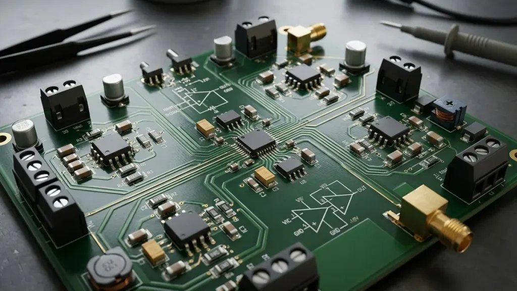
Op-Amp Signal Amplifier Board PCB Layout for Stability and Noise Control
PCB layout affects the parasitic resistance, capacitance, and inductance around an operational amplifier. These parasitic elements can influence noise coupling, feedback stability, bandwidth, settling behavior, and precision.
The most sensitive areas are generally the amplifier input nodes, feedback network, power supply connections, and output path.
Important layout considerations include:
- Keeping high-impedance input traces short and away from noisy switching nodes.
- Placing feedback components close to the amplifier pins to reduce unwanted parasitic capacitance.
- Avoiding parallel routing between sensitive input signals and high-current or fast-switching traces.
- Reviewing return-current paths rather than relying only on visual separation between signal traces.
- Placing decoupling components near the relevant supply pins.
- Checking whether output load capacitance can affect amplifier stability.
- Reviewing connector placement and external cable coupling for sensitive analog inputs.
For high-speed or wideband amplifier circuits, feedback path geometry and nearby return-current structures can become particularly important. The board stackup and trace configuration should be reviewed against the actual operating frequency and circuit requirements.
A critical distinction for procurement teams is that PCB fabrication accuracy supports the intended geometry, but it cannot correct an unsuitable circuit topology or an inherently unstable amplifier design.
For designs that include high-speed interfaces or demanding controlled-impedance connections, refer to the High-Speed PCB manufacturing page.
5. Grounding and Power Supply Decoupling Design
Grounding and power supply decoupling should be designed around actual current paths and the sensitivity of the analog signal nodes.
A ground plane can provide a low-impedance return path, but splitting every analog and digital ground area is not a universal solution. The design must account for current flow, analog-to-digital conversion, and the way different circuit sections share their return paths.
| Design item | Engineering consideration |
|---|---|
| Analog ground | Identify sensitive analog return paths |
| Digital ground | Prevent digital switching currents from disturbing analog references |
| Ground plane | Avoid unnecessary gaps and return-current detours |
| Supply bypass capacitors | Follow amplifier manufacturer placement and value recommendations |
| Feedback network | Minimize unwanted parasitic coupling |
| ADC interface | Review analog and digital current paths around the converter |
| Power entry | Consider bulk and high-frequency decoupling requirements |
| External connections | Evaluate shielding, grounding, and cable-related interference |
The appropriate bypass capacitor values and placement depend on the selected amplifier IC and its datasheet. Texas Instruments’ op-amp layout guidance discusses local bypass capacitors, short sensitive input traces, and grounding considerations. These recommendations should be applied in the context of the actual device and circuit rather than treated as universal rules.
For mixed-signal designs, analog and digital signal placement should be reviewed together with the converter and its interface. The objective is to control unwanted coupling and preserve predictable return-current paths, not simply to create visually separate copper areas.
For projects requiring controlled-impedance structures, the relevant PCB stackup and routing specifications should be confirmed during engineering review.
6. PCB Materials and Layer Stackup Selection for Precision Amplifiers
PCB material and layer-stackup selection should be based on signal frequency, impedance requirements, operating temperature, mechanical constraints, copper requirements, and circuit sensitivity.
For many general-purpose Op-Amp boards, standard FR-4 may be sufficient. More specialized materials should be considered only when electrical or environmental requirements justify them.
| PCB requirement | Material or stackup consideration | Design objective |
|---|---|---|
| General-purpose analog amplification | Standard FR-4 | Cost-effective fabrication |
| Industrial temperature exposure | Suitable high-Tg FR-4 grade | Thermal and dimensional stability |
| Wideband signal paths | Material with appropriate dielectric properties | Controlled high-frequency behavior |
| High-density component placement | Multilayer or HDI structure when justified | Routing and interconnection density |
| Controlled-impedance interface | Characterized dielectric and copper stackup | Impedance control |
| Mechanical or thermal constraints | Material and copper structure selected for the application | Board reliability |
A two-layer board may be appropriate for a relatively simple amplifier circuit. A four-layer or more complex stackup may be useful when the design requires additional routing space, a continuous reference plane, shielding strategies, or separation of functional sections.
However, adding layers does not automatically improve noise performance. An inappropriate stackup can create difficult return-current paths or increase manufacturing cost without providing a measurable benefit.
For high-frequency applications, PCBKR also provides High-Frequency PCB manufacturing capabilities. Material selection should be confirmed against the circuit’s frequency range and electrical specifications.
7. Advanced PCB Manufacturing Processes for Op-Amp Board Quality
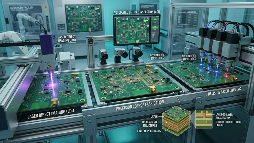
Advanced PCB Manufacturing Processes for Op-Amp Signal Amplifier Board Quality
Advanced PCB manufacturing processes help reproduce the copper patterns, layer structures, drilled features, and registration requirements specified by the engineering design. Their value depends on whether the Op-Amp board actually needs those capabilities.
For most precision amplifier boards, the main manufacturing objective is not maximum miniaturization. It is consistent fabrication of the specified geometry and stackup, together with appropriate inspection and process control.
| Manufacturing process or capability | PCBKR capability reference | Potential value to amplifier board projects |
|---|---|---|
| Laser Direct Imaging (LDI) | 8 µm target / ±10 µm stated capability | Supports fine-pattern imaging requirements |
| UV/CO₂ laser drilling | 75 µm ±5 µm stated capability | Supports specified microvia structures |
| Picosecond laser processing | 50 µm stated capability | Supports selected fine-feature applications |
| mSAP fabrication | 8/8 µm capability stated since Q3 2024 | Supports high-density fine-line designs |
| Multilayer lamination | LAUFFER process at 80/150/200 psi; vacuum below 50 mbar | Supports specified multilayer structures |
| Process capability control | Cpk target ≥1.33 | Provides a process-control target where applicable |
These capabilities are not mandatory specifications for every Op-Amp board. A conventional two-layer amplifier board may not need mSAP, microvias, or fine-line processing.
For a compact amplifier module with fine-pitch components, dense routing, or a complex mixed-signal structure, advanced fabrication processes may become relevant. The manufacturer should review the actual design rules, copper distribution, layer registration, via structure, and production quantity before recommending a process.
PCBKR’s inspection resources include 3D AOI, X-ray, and four-wire Kelvin flying-probe testing. These methods address different manufacturing inspection requirements. They do not, by themselves, establish that an assembled amplifier meets its specified gain, noise, offset, or frequency-response requirements.
For projects requiring dense routing or microvia structures, refer to the HDI PCB manufacturing page.
8. PCB Surface Contamination and Thermal Effects in Precision Op-Amp Circuits
PCB surface contamination and temperature gradients can affect high-impedance and precision DC amplifier circuits, even when the board passes ordinary visual inspection and electrical continuity testing.
This is particularly important for photodiode amplifiers, electrometer circuits, low-current sensor interfaces, and precision measurement equipment.
Surface Contamination and Leakage Current
Flux residues, moisture, dust, and other contamination can reduce surface insulation resistance. Leakage current across the PCB surface may create an unwanted voltage error at a high-impedance input.
Microchip’s precision op-amp design guidance explains how PCB surface resistance and bulk dielectric resistance can contribute to leakage errors. It also identifies high-impedance photodiode circuits as an important example.
Manufacturing and assembly reviews should consider:
- Whether the circuit contains high-impedance input nodes.
- Whether flux chemistry and assembly residues could affect the application.
- Whether a cleaning process is required by the customer’s design.
- Whether ionic contamination or insulation-resistance testing is required.
- Whether conformal coating is appropriate and compatible with the circuit.
- Whether moisture and environmental exposure are part of qualification requirements.
Cleaning, baking, coating, and other post-assembly treatments should not be applied automatically. They must be selected according to component datasheets, PCB materials, assembly processes, and customer requirements.
Thermal Gradients and Thermoelectric Voltage
Connections between dissimilar metals can generate thermoelectric voltages when temperature gradients exist. In precision circuits, these small voltages can become significant compared with the signal being measured.
Potential sources include connectors, solder joints, switches, resistors, sockets, and other dissimilar-metal junctions.
For procurement and engineering review, important considerations include whether the design has critical low-level inputs, whether heat-generating components are located near those inputs, and whether the assembly process preserves the required cleanliness and thermal conditions.
9. SMT Assembly and PCBA Reliability for Op-Amp Boards
SMT assembly affects component placement, solder-joint formation, electrical connections, and the repeatability of the completed PCBA.
For an Op-Amp Signal Amplifier Board, assembly quality is important because small passive components and sensitive amplifier inputs often form part of the gain, filtering, bias, and feedback networks.
| Assembly stage | Main concern | Relevant inspection or review |
|---|---|---|
| Incoming component verification | Correct IC, resistor, capacitor, and package | BOM and approved-part verification |
| Solder paste printing | Paste volume and alignment | SPI where specified |
| Component placement | Polarity, orientation, and position | Placement program and AOI |
| Reflow soldering | Solder-joint quality and thermal profile | Profile validation and visual inspection |
| Fine-pitch package assembly | Hidden solder-joint defects | X-ray where applicable |
| Post-assembly inspection | Missing, shifted, or incorrectly oriented components | AOI and manual inspection |
| Electrical verification | Opens, shorts, and connection integrity | Flying-probe or other agreed electrical tests |
For precision amplifier boards, component substitutions should be controlled carefully. A resistor with a different tolerance or temperature coefficient, or a capacitor with different dielectric behavior, can change the circuit’s electrical characteristics.
The assembly supplier should therefore follow the approved BOM and obtain customer authorization before making substitutions.
PCBKR supports PCB fabrication and PCBA assembly for customer-defined projects. SMT, through-hole assembly, and turnkey material sourcing can be evaluated according to the BOM, component availability, package types, and production requirements.
For boards combining analog amplification with embedded control functions, the Embedded Control Board OEM page provides an additional reference for related board manufacturing.
10. Inspection and Functional Testing for Op-Amp Signal Amplifier PCBA
An Op-Amp Signal Amplifier PCBA should be inspected at both the manufacturing level and, where required, the functional level.
The test plan must distinguish between checking whether the board has been fabricated and assembled correctly and verifying whether the amplifier performs according to its electrical specification.
| Test category | Typical method | What it can verify |
|---|---|---|
| Visual inspection | Manual inspection and AOI | Component presence, polarity, visible assembly defects |
| Hidden solder-joint inspection | X-ray | Selected hidden joints, such as applicable leadless packages |
| Electrical connectivity | Flying-probe or agreed electrical test | Opens, shorts, and specified net connectivity |
| Resistance and continuity | Multimeter or test fixture | Selected electrical paths |
| Supply current | Bench power supply and measurement equipment | Current consumption under defined conditions |
| DC offset | Precision measurement instrument | Output offset under specified conditions |
| Gain accuracy | Signal generator and measurement instrument | Gain at specified input and frequency |
| Frequency response | Network or frequency-response measurement setup | Response over the agreed frequency range |
| Noise measurement | Suitable low-noise measurement setup | Noise under defined bandwidth and measurement conditions |
| Stability verification | Oscilloscope and defined test load | Oscillation or transient behavior under specified conditions |
AOI, X-ray, and electrical connectivity tests cannot replace functional amplifier testing.
For example, a board may pass continuity testing but still have an incorrect gain because of a wrong resistor value. It may also show unstable behavior under a particular load even though the solder joints are acceptable.
Before production, the customer and manufacturer should agree on:
- Test input amplitude and waveform.
- Supply voltage and current limits.
- Output load and measurement points.
- Gain and offset acceptance limits.
- Required frequency range and bandwidth.
- Noise measurement bandwidth and test conditions.
- Test fixture, instrument requirements, and reporting format.
Functional testing should only be claimed when the required test equipment, fixtures, procedures, and acceptance limits have been agreed and are available for the project.
11. Op-Amp PCB Manufacturer and PCBA Supplier Evaluation Criteria
Buyers should evaluate an Op-Amp PCB supplier based on its ability to understand circuit requirements, manufacture the specified board, control assembly quality, and provide appropriate verification for the intended application.
A low quotation alone is not sufficient to establish supplier suitability.
| Evaluation item | Questions buyers should ask |
|---|---|
| Engineering review | Can the supplier review Gerber, BOM, schematic, and stackup data? |
| PCB fabrication | Can the supplier meet the specified layer count, copper thickness, dimensions, and tolerances? |
| Material sourcing | Can the supplier follow approved PCB material and component specifications? |
| SMT assembly | Can the supplier assemble the specified IC packages and passive components? |
| Component traceability | Can component batches and approved substitutions be documented? |
| Inspection | Are AOI, X-ray, and electrical testing available where applicable? |
| Functional testing | Can the supplier support the agreed amplifier test requirements? |
| Production flexibility | Can the supplier handle prototype, small-batch, and production orders? |
| Quality documentation | Can the supplier provide agreed inspection and production records? |
| Change control | How are BOM, drawing, material, and process changes approved? |
For precision analog boards, buyers should also discuss surface cleanliness, high-impedance node protection, handling, storage, and the need for special post-assembly processes.
A useful supplier comparison should separate three different cost categories:
- PCB fabrication cost.
- PCBA assembly and component sourcing cost.
- Additional inspection, functional testing, and documentation cost.
This makes it easier to compare quotations without confusing a basic assembly offer with a fully tested PCBA supply arrangement.
12. Op-Amp Signal Amplifier Board RFQ and Quotation Requirements
A complete RFQ package helps the manufacturer assess manufacturability, material requirements, assembly complexity, inspection needs, and production cost.
Buyers should provide as much of the following information as possible.
| RFQ information | Recommended details |
|---|---|
| Product name | Op-Amp Signal Amplifier Board |
| Gerber or ODB++ | Complete fabrication data |
| PCB stackup | Layer count, thickness, copper weight, material |
| PCB dimensions | Length, width, board thickness, tolerances |
| Surface finish | ENIG, HASL, OSP, or other specified finish |
| Schematic | Circuit architecture and signal connections |
| BOM | Part number, manufacturer, package, quantity |
| Assembly drawing | Component location, polarity, special instructions |
| Component requirements | Approved manufacturers and substitution restrictions |
| Electrical specifications | Gain, offset, bandwidth, noise, supply voltage |
| Testing requirements | AOI, X-ray, electrical, and functional test requirements |
| Quantity | Prototype, small batch, pilot, or mass production |
| Delivery requirements | Target lead time and shipping destination |
For sensitive analog circuits, buyers should also identify high-impedance input nodes, low-level signal requirements, operating temperature, environmental exposure, and any special cleaning or coating requirements.
Recommended RFQ Document Package
For an accurate quotation, prepare the following documents whenever available:
- Gerber or ODB++ fabrication files.
- BOM with manufacturer part numbers.
- Assembly drawings and schematic.
- PCB stackup and material requirements.
- Required quantities and target delivery schedule.
- Electrical and functional acceptance criteria.
If the design is still under development, the RFQ can begin with available design files and a description of unresolved engineering requirements. The manufacturer can then review the information needed for a more complete quotation.
13. Shenzhen Hongda Circuit Technology PCB and PCBA Manufacturing Capabilities
Shenzhen Hongda Circuit Technology Co., Ltd. supports custom PCB fabrication and PCBA assembly for OEM customers developing analog signal-processing, sensor-interface, industrial-control, and electronic measurement products.
For Op-Amp Signal Amplifier Board projects, the manufacturing approach should be based on the customer’s circuit architecture and production requirements rather than a fixed, one-size-fits-all board configuration.
PCB Fabrication and Inspection Resources
| Capability | Application to customer projects |
|---|---|
| PCB fabrication | Custom board dimensions, layer structures, copper specifications, and material requirements |
| LDI imaging | Fine-pattern fabrication according to specified design rules |
| Multilayer lamination | Production of specified multilayer PCB structures |
| Laser drilling | Selected microvia and fine-feature requirements |
| mSAP processing | High-density fine-line designs when required |
| SMT and through-hole assembly | Assembly according to approved BOM and drawings |
| 3D AOI | Visual inspection of assembled components and solder joints |
| X-ray inspection | Inspection of applicable hidden solder joints |
| Four-wire Kelvin flying probe | Electrical testing for specified PCB connectivity requirements |
The correct manufacturing process depends on the project. A general-purpose amplifier board may use a conventional PCB structure, while a compact mixed-signal design may require additional routing density, controlled impedance, or specialized fabrication processes.
PCBKR’s manufacturing resources can be evaluated against the actual Gerber data, stackup, BOM, component packages, inspection plan, and production volume.
Prototype, Small-Batch, and Mass Production Support
A practical production workflow can include:
- RFQ and engineering review: Review fabrication files, BOM, stackup, and acceptance requirements.
- DFM and assembly review: Identify manufacturing constraints and confirm component and package requirements.
- Prototype production: Manufacture and assemble the initial quantity for customer evaluation.
- Engineering validation: Verify the agreed electrical and assembly requirements.
- Design and process confirmation: Confirm approved files, materials, BOM, and production instructions.
- Production planning: Establish the manufacturing and inspection plan for repeat orders.
- Production and quality review: Follow the agreed inspection and documentation requirements.
The customer remains responsible for defining the circuit’s intended electrical performance and acceptance limits. PCBKR’s role is to manufacture and assemble the board according to the approved design and agreed production requirements.
Custom Op-Amp PCB and PCBA Quotation
For OEM customers sourcing custom Op-Amp Signal Amplifier Boards, PCB fabrication, or turnkey PCBA assembly, Shenzhen Hongda Circuit Technology can review the available design files and project requirements.
Send the Gerber files, BOM, schematic, target quantity, and technical requirements for manufacturing evaluation.
Shenzhen Hongda Circuit Technology Co., Ltd.
Email: sales@pcbkr.com
Website: https://www.pcbkr.com
Contact our team to discuss prototype, small-batch, and production requirements for custom analog amplifier PCB and PCBA projects.
Frequently Asked Questions
Can You Manufacture Custom Op-Amp Signal Amplifier Boards from Gerber and BOM Files?
Customers can provide Gerber or ODB++ fabrication data, BOM, assembly drawings, and relevant technical specifications for manufacturing review. A schematic is also useful when the project includes sensitive analog nodes or special electrical requirements.
Do You Provide Both PCB Fabrication and Complete PCBA Assembly?
PCB fabrication and PCBA assembly can be evaluated together according to project requirements. SMT, through-hole assembly, and turnkey component sourcing can be discussed based on the approved BOM, component availability, and assembly specifications.
Can You Manufacture Low-Noise and Precision Op-Amp Amplifier Boards?
PCBKR can review the fabrication and assembly requirements associated with low-noise and precision amplifier designs. Buyers should provide relevant circuit information, including input impedance, signal level, gain, offset, bandwidth, cleanliness requirements, and special environmental conditions. Actual electrical performance must be verified against agreed test criteria.
What Inspection and Functional Testing Are Available for Op-Amp Signal Amplifier PCBA?
Available inspection resources include 3D AOI, X-ray inspection, and four-wire Kelvin flying-probe testing. Functional tests such as gain, offset, noise, and frequency response require defined test conditions, suitable instruments, and agreed acceptance limits.
Do You Support Prototype, Small-Batch, and Mass Production?
Prototype, small-batch, and production requirements can be reviewed according to PCB design, BOM, assembly complexity, material availability, and delivery schedule. Customers should provide target quantities and required production milestones when requesting a quotation.
Op-Amp Signal Amplifier Board | Data Sheet
| Parameter | Specification |
|---|---|
| Product Type | Op-Amp Signal Amplifier Board |
| PCB Type | Rigid PCB |
| PCB Material | FR-4 / High-Tg FR-4 / Custom Material |
| Layer Count | 2–8 Layers / Custom |
| Board Thickness | 0.8–2.0 mm / Custom |
| Copper Thickness | 1–3 oz / Custom |
| Minimum Trace Width / Spacing | According to Design Requirements |
| Minimum Drill Size | According to Design Requirements |
| Surface Finish | ENIG / HASL / OSP / Custom |
| Solder Mask | Green / Blue / Black / White / Custom |
| Silkscreen | White / Black / Custom |
| Amplifier IC Type | General-Purpose / Precision / Instrumentation / Low-Noise Op-Amp |
| Amplifier Configuration | Inverting / Non-Inverting / Buffer / Differential / Transimpedance |
| Signal Type | Analog / Low-Level / Differential |
| Operating Voltage | According to Op-Amp IC and Circuit Design |
| Signal Gain | Customizable According to Circuit Design |
| Frequency Response | According to Amplifier IC and Circuit Design |
| Input Impedance | According to Circuit Design |
| Output Load | According to Circuit Design |
| Noise Performance | According to Selected IC and Circuit Design |
| Component Package | SMD / Through-Hole / Mixed |
| Assembly Process | SMT / THT / Mixed Assembly |
| PCB Inspection | AOI / Electrical Testing |
| PCBA Inspection | AOI / X-ray / Visual Inspection |
| Functional Testing | Optional, According to Customer Test Specifications |
| Application | Sensor Signal Conditioning / Instrumentation / Data Acquisition / Industrial Measurement / Audio |
| Production Volume | Prototype / Small Batch / Mass Production |
| Customization | PCB Fabrication / Component Sourcing / PCBA Assembly |
About Author
David Chen LinkedIn Profile
David Chen is a Senior RF/PCB Process Engineer at Shenzhen Hongda Circuit Technology Co., Ltd., with over 12 years of experience in high-frequency PCB fabrication, impedance-controlled stack-up design, and Rogers/PTFE laminate processing. He also boasts an extensive professional background in PCBA manufacturing, PCBA testing, and PCBA optimization, with specialized expertise in high-precision PCBA fault analysis and rigorous PCBA reliability testing. The author has worked with high-layer-count server PCB fabrication, ultra-low-loss backplane stackups, and thermo-mechanical reliability optimization for AI infrastructure projects involving 112G and 224G PAM4 architectures. Skilled in complex circuit design and cutting-edge advanced PCB manufacturing processes, he delivers solutions that elevate product durability and performance across industrial applications. His technical articles focusing on PCBA manufacturing workflows and testing methodologies are widely cited by industry peers and technical platforms, and have gained attention and recognition from industry colleagues.