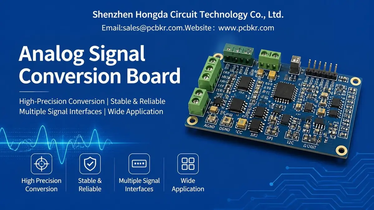
Analog Signal Conversion Board Manufacturing for OEM Projects
PCB Material:FR-4 / High-Tg FR-4
Layer Count:2–8 Layers
Board Thickness:0.8–2.0 mm
Copper Thickness:1–2 oz
Min. Trace Width / Spacing:0.10 / 0.10 mm
Min. Drill Diameter:0.20 mm
An Analog Signal Conversion Board converts real-world voltage or current signals into digital data, or converts digital control data into analog outputs through ADC and DAC circuits. For OEM equipment manufacturers, reliable board performance depends on more than converter specifications. Signal conditioning, reference voltage stability, PCB layout, power integrity, component selection, and PCBA manufacturing quality all affect the final result. Selecting a qualified PCB and PCBA manufacturing partner helps reduce design risks, improve production consistency, and support a smoother transition from prototype development to mass production.
Analog Signal Conversion Board Overview
An Analog Signal Conversion Board is an electronic circuit board designed to convert, condition, and transmit analog signals between external devices and digital electronic systems. Its main functions typically include analog-to-digital conversion (ADC), digital-to-analog conversion (DAC), voltage or current signal conditioning, filtering, buffering, and input or output protection.
These boards are used in electronic equipment that needs to acquire physical measurements, process analog information, or generate controlled analog signals. Depending on the application, a conversion board may contain one or more ADC or DAC devices, operational amplifiers, voltage references, filters, protection components, and digital communication interfaces.
Core Functions of Analog Signal Conversion Boards
The specific circuit architecture depends on the application and the required signal characteristics.
| Functional block | Main purpose | Typical circuit elements |
|---|---|---|
| Analog input | Receives external analog signals | Connectors, protection components |
| Signal conditioning | Adjusts signal amplitude and bandwidth | Operational amplifiers, resistors, capacitors |
| Analog-to-digital conversion | Converts analog signals into digital data | ADC devices |
| Digital-to-analog conversion | Generates analog outputs from digital data | DAC devices |
| Voltage reference | Provides a stable conversion reference | Precision reference ICs |
| Power management | Supplies required circuit voltages | Regulators, filters, decoupling capacitors |
| Digital interface | Transfers conversion results or control data | SPI, I²C, parallel interfaces |
A basic conversion board may contain only an ADC and its supporting circuits. More complex designs can integrate multiple conversion channels, signal conditioning stages, digital control logic, and different power supply domains.
Typical Applications
Analog Signal Conversion Boards are used in electronic products where accurate analog measurement or controlled analog output is required.
Common applications include:
- Industrial measurement instruments.
- Laboratory and test equipment.
- Data acquisition equipment.
- Precision voltage and current monitoring.
- Power electronics measurement and control.
- Sensor-based electronic instruments.
- Automated testing equipment.
- Embedded measurement and control products.
For metering applications involving voltage and current measurement, see smart meter PCB manufacturing.
The required circuit architecture varies according to the signal source, operating environment, measurement range, and system-level performance requirements.
Analog Signal Conversion Architecture and Operating Principles
An Analog Signal Conversion Board generally uses an ADC signal path, a DAC signal path, or a combination of both. The architecture determines how signals enter the board, how they are conditioned, and how conversion data is transferred to the host system.
Analog-to-Digital Conversion
An ADC converts a continuous analog input into a digital representation that a processor or digital control system can read.
A typical signal path consists of:
- Analog input connector.
- Input protection and filtering.
- Signal amplification or attenuation.
- ADC input driver.
- ADC conversion stage.
- Digital interface to the controller.
The analog input must remain within the converter’s specified input range. If the external signal exceeds this range, an appropriate attenuation or protection circuit may be required.
The input signal bandwidth must also be considered. For sampled systems, the sampling frequency needs to be selected according to the signal bandwidth and the required reconstruction or measurement performance. Anti-aliasing filtering is commonly used to reduce unwanted frequency components before conversion.
Digital-to-Analog Conversion
A DAC converts digital data into a corresponding analog voltage or current output.
A typical DAC signal path includes:
- Digital data input.
- DAC device.
- Reference voltage or current.
- Output buffer or amplifier.
- Reconstruction filtering, where required.
- Analog output connector.
The output circuit must be designed around the required voltage or current range, load impedance, settling time, output drive capability, and accuracy.
For example, a DAC intended to drive a high-impedance measurement input may require a different output stage from one intended to drive a relatively low-impedance external circuit.
Voltage and Current Signal Conversion
Analog signal conversion boards may process voltage signals, current signals, or both.
Voltage inputs require suitable scaling, buffering, filtering, and protection based on their specified range and source impedance.
Current inputs may use a precision shunt resistor or another appropriate current-sensing circuit to produce a voltage that can be processed by the ADC. The selection of the sensing resistor affects voltage drop, power dissipation, measurement range, and error contribution.
The circuit design should account for:
- Minimum and maximum input values.
- Expected signal bandwidth.
- Source impedance.
- Common-mode voltage.
- Input protection requirements.
- Measurement accuracy targets.
- Environmental operating conditions.
These parameters should be confirmed before PCB layout and component selection.
Multi-Channel Signal Conversion
Multi-channel conversion boards are designed to process multiple analog inputs or outputs on one PCB.
Two common ADC architectures are multiplexed conversion and simultaneous sampling.
| Architecture | Operating principle | Main design consideration |
|---|---|---|
| Multiplexed ADC | Multiple inputs share one converter through a multiplexer | Channel switching time and settling behavior |
| Simultaneous-sampling ADC | Multiple channels are sampled at approximately the same time | Channel matching and synchronization |
| Multiple independent ADCs | Separate converters process different input channels | Clock coordination and channel consistency |
The appropriate architecture depends on the required channel count, sampling rate, timing relationship, cost target, and available PCB space.
For applications involving phase comparison or synchronized measurements, channel timing differences may be as important as nominal sampling rate.
ADC and DAC Specifications for OEM Board Selection
Converter specifications directly affect board performance, but individual data-sheet values should not be treated as guaranteed system-level measurement results.
OEM buyers should evaluate the complete signal chain rather than selecting a converter solely by resolution or maximum sampling rate.
ADC Resolution and Actual Measurement Accuracy
ADC resolution describes the number of discrete digital output levels available to represent an analog input.
For an ideal N-bit converter, the number of quantization levels is:
Number of quantization levels = 2^N
For example:
- 12-bit ADC: 4,096 quantization levels.
- 16-bit ADC: 65,536 quantization levels.
- 24-bit ADC: 16,777,216 quantization levels.
A higher bit count provides more theoretical resolution. However, it does not automatically guarantee higher measurement accuracy.
Actual board-level performance can also be affected by:
- ADC offset error.
- Gain error.
- Integral nonlinearity (INL).
- Differential nonlinearity (DNL).
- Reference voltage tolerance and drift.
- Analog input noise.
- Power supply noise.
- PCB leakage and grounding.
- Component temperature characteristics.
For this reason, an OEM specification should distinguish between nominal ADC resolution and the required system-level accuracy.
| Parameter | Meaning | Procurement consideration |
|---|---|---|
| Resolution | Number of available digital levels | Required measurement granularity |
| Accuracy | Difference between measured and actual values | Overall error budget |
| INL | Deviation from an ideal transfer function | Conversion linearity |
| DNL | Deviation of individual code widths | Code uniformity |
| SNR | Signal-to-noise ratio | Measurement noise performance |
| ENOB | Effective number of bits | Practical dynamic performance |
| Offset error | Output deviation near zero input | Low-level measurement accuracy |
| Gain error | Difference in conversion scale | Full-scale measurement accuracy |
The required accuracy should be defined at the board level whenever possible, with the test conditions and measurement range specified.
Sampling Rate and Signal Bandwidth
Sampling rate describes how frequently an ADC captures an input signal.
The required sampling rate depends on the input bandwidth, signal characteristics, filtering, and measurement objective.
For a band-limited signal, the Nyquist sampling principle requires the sampling frequency to exceed twice the highest frequency component. Practical systems often require additional margin and appropriate analog filtering.
OEM buyers should specify:
- Maximum input signal frequency.
- Required sampling rate per channel.
- Total system sampling throughput.
- Number of active channels.
- Simultaneous or multiplexed sampling requirements.
- Required synchronization accuracy.
- Anti-aliasing filter characteristics.
A converter advertised with a high aggregate sampling rate may not deliver that same rate independently to every channel. This distinction should be confirmed during design review.
Input and Output Voltage Ranges
The ADC input range and DAC output range must match the electrical requirements of the target equipment.
Typical voltage ranges may include unipolar and bipolar configurations. The final range depends on the converter, reference voltage, analog front-end, and power supply architecture.
For each input or output channel, the specification should define:
- Minimum and maximum voltage.
- Expected normal operating range.
- Absolute maximum input limits.
- Input impedance or output load.
- Common-mode voltage, where applicable.
- Required protection level.
- Accuracy over the specified range.
A mismatch between external signal levels and the converter input range can cause clipping, measurement errors, or component damage.
Reference Voltage Stability and Conversion Linearity
The ADC reference voltage establishes the scale used to interpret the input signal. A variation in reference voltage can therefore introduce conversion errors.
Reference voltage design should consider:
- Initial reference accuracy.
- Temperature coefficient.
- Long-term drift.
- Output noise.
- Load regulation.
- Decoupling requirements.
- PCB routing and return paths.
The reference source should be selected according to the required accuracy and the converter’s electrical characteristics.
For precision applications, the reference circuit should be reviewed together with the ADC input stage, power supply, and PCB layout. Treating the reference voltage as an isolated component selection can overlook important error sources.
Single-Ended and Differential Inputs
Single-ended and differential input architectures serve different signal acquisition requirements.
| Input configuration | Characteristics | Typical consideration |
|---|---|---|
| Single-ended | Signal measured relative to a reference ground | Simpler interface and lower circuit complexity |
| Differential | Difference between two input signals is measured | Better suitability for certain common-mode noise environments |
Differential inputs can improve noise rejection when the source, input circuitry, and PCB layout are designed appropriately. They do not automatically eliminate interference or grounding problems.
The input configuration should match the signal source and the common-mode voltage conditions.
Signal Conditioning for Stable Analog Conversion
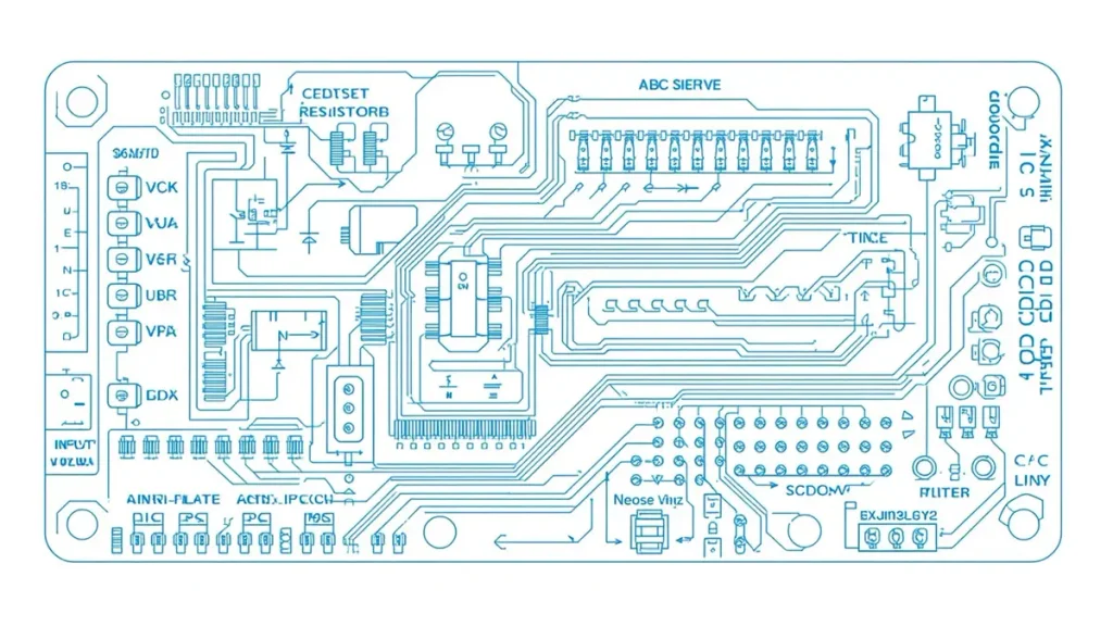
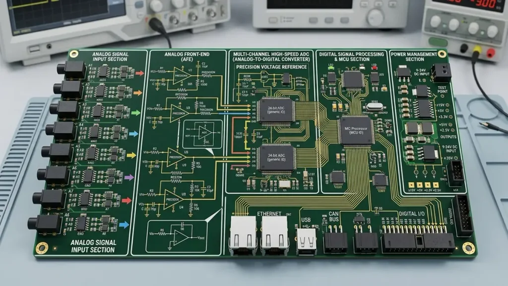
Signal conditioning stages showing amplification, buffering, filtering, and input protection for stable analog conversion.
Signal conditioning prepares an analog signal for accurate conversion. It helps ensure that the signal presented to the ADC or generated by the DAC remains within the electrical and dynamic requirements of the converter.
Operational Amplifier Circuits
Operational amplifiers are frequently used in analog front-end circuits.
Their functions may include:
- Signal amplification.
- Voltage attenuation through suitable circuit configurations.
- Buffering.
- Differential signal conditioning.
- Active filtering.
- Output driving.
The selected amplifier must be compatible with the ADC or DAC input requirements.
Important parameters include input offset voltage, input bias current, noise density, gain bandwidth, slew rate, output swing, common-mode range, and settling time.
An amplifier with an unsuitable output stage may introduce settling errors or distortion, even when the ADC itself has sufficient resolution.
Input Scaling and Buffering
Input scaling adjusts an external signal to fit the converter’s usable input range.
A resistor network may be used for attenuation, while an amplifier stage can provide gain or buffering where required.
The design should consider resistor tolerance, temperature coefficient, amplifier errors, source impedance, and loading effects.
Buffer circuits can reduce the influence of the signal source impedance on the ADC input. However, the buffer must be stable with the capacitive loading and sampling behavior of the selected converter.
Low-Pass and Anti-Aliasing Filters
Filtering controls the frequency content entering the conversion stage.
A low-pass filter may reduce unwanted high-frequency noise, while an anti-aliasing filter helps limit frequency components that could otherwise appear as false lower-frequency signals after sampling.
The filter design depends on:
- Signal bandwidth.
- ADC sampling rate.
- Required passband flatness.
- Stopband attenuation.
- Phase response.
- Component tolerance.
- Filter settling requirements.
The filter should be designed as part of the complete signal chain rather than added without considering the ADC’s input behavior.
Input Protection and Electrical Reliability
External analog inputs may be exposed to overvoltage, electrostatic discharge, transient events, or incorrect connections.
Protection design can include suitable series resistors, clamping devices, transient suppression components, and current-limiting circuits.
Protection components must be selected according to the normal signal range and the expected abnormal conditions. Their leakage current, capacitance, clamping voltage, and response characteristics may affect measurement performance.
The protection circuit should be validated against the actual operating environment and interface requirements.
PCB Layout Factors Affecting Analog Conversion Performance
PCB layout influences noise coupling, signal integrity, reference stability, and power distribution. A well-selected ADC can still produce unsatisfactory results if the supporting PCB layout introduces excessive interference or unstable signal paths.
Analog and Digital Circuit Placement
Analog input circuits and high-speed digital circuits should be positioned according to their noise sensitivity and signal relationships.
Sensitive analog input paths should be kept away from noisy switching nodes, fast digital interfaces, and high-current paths where practical.
The layout should consider:
- ADC placement relative to the analog front end.
- Separation of sensitive inputs from switching regulators.
- Short and controlled reference voltage connections.
- Appropriate placement of decoupling capacitors.
- Digital interface routing.
- Connector locations and external signal paths.
Placement should be planned before routing begins because later changes can be difficult to implement without affecting other circuit requirements.
Grounding and Return-Current Paths
Grounding is a major consideration in mixed-signal PCB design.
The objective is to provide appropriate return-current paths while minimizing unwanted coupling between sensitive analog signals and noisy digital or power circuits.
Grounding decisions should be based on the actual current paths, converter recommendations, PCB stackup, and circuit topology.
A split ground plane is not automatically better than a continuous ground plane. Poorly positioned splits can force return currents to take longer paths and increase interference.
For many mixed-signal designs, a carefully planned continuous reference plane with appropriate component placement and routing can provide a more predictable return path.
Reference Voltage Routing
Reference voltage routing should minimize unwanted resistance, noise coupling, and interference from switching signals.
Important layout practices include:
- Keeping reference paths short where practical.
- Placing required decoupling components close to their associated pins.
- Avoiding unnecessary routing near high-noise switching nodes.
- Providing suitable return paths.
- Following the converter and reference IC manufacturer’s layout recommendations.
The reference circuit should also be protected from unnecessary loading and thermal gradients that may affect its stability.
Power Supply Noise Control
ADC, DAC, amplifier, and reference circuits may have different power supply requirements.
The PCB power architecture should account for:
- Analog and digital supply requirements.
- Switching regulator noise.
- Linear regulator performance.
- Power supply sequencing, where applicable.
- Local decoupling.
- Current return paths.
- Thermal behavior.
Power filtering should be selected according to the frequency characteristics of the noise and the load requirements. Adding ferrite beads or capacitors without considering impedance and resonance can create unexpected behavior. For related power-board fabrication considerations, see PCB for power supply.
Crosstalk and Electromagnetic Interference
Unwanted coupling can occur through electric fields, magnetic fields, shared impedance, and common return paths.
Sensitive analog inputs should be routed with appropriate spacing and reference-plane support. High-speed digital lines and switching power traces should be routed with attention to their potential impact on measurement channels.
For differential signals, routing symmetry and consistent electrical conditions can help preserve signal balance.
The exact routing rules depend on signal bandwidth, voltage levels, impedance requirements, stackup, and board geometry.
PCB Manufacturing and PCBA Quality for Analog Signal Conversion Boards
Circuit design establishes the intended electrical performance, while PCB fabrication and PCBA assembly determine whether the physical board can reproduce that design consistently.
For OEM projects, manufacturing review should cover more than board dimensions and basic electrical continuity. It should also verify the fabrication and assembly details that affect sensitive analog circuits.
PCB Stackup and Ground-Plane Continuity
The PCB stackup determines the arrangement of signal, ground, and power layers.
A suitable stackup can support predictable return paths, reduce unwanted coupling, and provide appropriate routing space for analog and digital circuits.
The stackup review should consider:
- Total number of layers.
- Board thickness.
- Copper thickness.
- Ground-plane arrangement.
- Power distribution.
- Signal routing requirements.
- Via structures.
- Manufacturing tolerances.
For multi-layer conversion boards, the stackup should be reviewed together with the component placement and routing plan.
Copper Thickness, Trace Geometry, and Via Quality
Copper thickness and trace geometry affect resistance, current capacity, and electrical behavior.
For sensitive analog circuits, trace routing should also account for signal integrity, parasitic capacitance, parasitic inductance, and coupling.
Via structures should be selected according to the signal path, layer transitions, current requirements, and manufacturing capability.
Manufacturing review should confirm that the specified trace width, spacing, annular ring, hole size, and registration requirements are compatible with the selected fabrication process.
SMT Assembly and Component Placement
PCBA assembly quality directly affects electrical connections and long-term reliability.
For Analog Signal Conversion Boards, particular attention should be given to precision resistors, reference ICs, ADC/DAC devices, operational amplifiers, and other sensitive components.
Important assembly considerations include:
- Component orientation and polarity.
- Correct BOM part numbers.
- Component package compatibility.
- Solder paste printing.
- Placement accuracy.
- Reflow profile control.
- Solder joint quality.
- Moisture-sensitive component handling where applicable.
A substitution that appears electrically similar may have different noise, tolerance, temperature, or settling characteristics. Component substitutions should therefore be reviewed and approved before production.
Inspection and Electrical Testing
Inspection and testing should be selected according to the product design and the customer’s quality requirements.
Common manufacturing quality controls include:
| Inspection or test | Main purpose |
|---|---|
| Incoming material inspection | Checks component and material conformity |
| Solder paste inspection, where applicable | Checks printed solder paste quality |
| 3D AOI | Inspects visible assembly and soldering conditions |
| X-ray inspection | Examines hidden solder joints, such as suitable BGA connections |
| Electrical continuity testing | Checks electrical connections and opens/shorts |
| Flying probe testing | Supports electrical testing of suitable PCB designs |
| Functional testing | Verifies defined board-level functions |
| Calibration, where specified | Checks performance against agreed reference conditions |
AOI and X-ray inspection cannot replace functional testing. Similarly, electrical continuity testing does not prove that an ADC meets its required measurement accuracy.
For precision conversion boards, functional verification may need to include defined input levels, output measurements, reference conditions, and test limits.
The test plan should be agreed before production so that the supplier and buyer share the same acceptance criteria.
Prototype-to-Production Consistency
A prototype that works in the laboratory does not automatically guarantee consistent mass production.
The transition to production should include review of:
- Approved Gerber and assembly files.
- Controlled BOM revisions.
- Approved component substitutions.
- PCB stackup and fabrication notes.
- Assembly process requirements.
- Inspection criteria.
- Functional test procedures.
- Engineering change records.
A controlled manufacturing process helps reduce differences between prototype, pilot production, and subsequent batches.
OEM Procurement Requirements for Analog Signal Conversion Boards
A complete RFQ allows a PCB and PCBA supplier to evaluate the technical requirements, manufacturing process, material selection, and testing scope before quotation.
Incomplete specifications can lead to repeated engineering clarification, inaccurate pricing, unsuitable component selection, and production delays.
Technical Specification Checklist
OEM buyers should prepare the following information wherever available.
| RFQ item | Information to provide |
|---|---|
| Product application | Intended equipment and operating environment |
| ADC/DAC device | Required part number or performance target |
| Resolution | Required converter resolution |
| Accuracy | Required board-level accuracy and test conditions |
| Sampling rate | Per-channel rate and total throughput |
| Channel count | Number of analog input and output channels |
| Input range | Voltage or current range |
| Output range | Required DAC voltage or current range |
| Input configuration | Single-ended or differential |
| Reference voltage | Required source and tolerance |
| Power supply | Voltage rails and current requirements |
| PCB specifications | Layer count, thickness, copper weight, dimensions |
| Assembly files | Gerber, BOM, pick-and-place and assembly drawings |
| Testing requirements | Electrical, functional, calibration or other specified tests |
| Production quantity | Prototype, pilot batch or mass production |
| Delivery requirements | Target lead time and packaging requirements |
Not every project needs every item at the initial RFQ stage. However, the more complete the information, the more accurately a supplier can assess feasibility and provide a quotation.
Manufacturing Cost Factors
The cost of a custom Analog Signal Conversion Board depends on its electrical design, PCB construction, components, assembly complexity, and testing requirements.
| Cost factor | Potential cost impact |
|---|---|
| ADC/DAC selection | Component price and availability |
| Precision components | Higher tolerance and performance requirements |
| PCB layer count | Material and fabrication complexity |
| Board dimensions | Material usage and panel utilization |
| Fine-pitch components | Assembly process and inspection requirements |
| Special materials | Material cost and process compatibility |
| Functional testing | Test fixtures, labor and validation time |
| Calibration | Reference equipment and test procedures |
| Order quantity | Setup cost allocation and purchasing efficiency |
A lower component or fabrication price does not necessarily produce the lowest total project cost. Poor component availability, insufficient testing, or repeated rework can increase the overall cost of ownership.
Supplier Evaluation Criteria
OEM buyers should assess a manufacturer’s engineering communication, fabrication capability, assembly process, and quality controls.
A practical supplier evaluation should include:
- Engineering review: Ability to review Gerber, BOM, stackup, and assembly requirements.
- PCB fabrication: Compatibility with required layer count, copper thickness, trace geometry, and board tolerances.
- Component sourcing: BOM verification, approved alternatives, and traceability requirements.
- PCBA assembly: SMT/THT process capability and inspection arrangements.
- Quality control: Defined inspection procedures and documented production controls.
- Testing support: Ability to perform the agreed electrical and functional tests.
- Production planning: Clear communication on prototype, pilot, and mass production schedules.
Buyers should request relevant process information and sample inspection or test records where appropriate. General statements about quality or advanced manufacturing should be supported by evidence relevant to the actual project.
Prototype Validation and Mass Production Readiness
Prototype production provides an opportunity to verify the circuit design, component selection, PCB layout, and assembly process before larger production runs.
A practical validation process can include:
- Visual inspection and assembly verification.
- Power-on checks.
- Input and output range verification.
- ADC/DAC functional checks.
- Noise and stability evaluation under defined conditions.
- Communication interface verification.
- Temperature-related testing where required.
- Customer approval of the validated configuration.
Once the prototype is approved, the production package should be controlled to maintain consistency across manufacturing batches.
The buyer and supplier should agree on the revision of the design files, BOM, test procedure, acceptance criteria, and any approved component alternatives.
PCBKR Analog Signal Conversion Board Manufacturing Support
Shenzhen Hongda Circuit Technology Co., Ltd. provides PCB fabrication and PCBA manufacturing services for OEM electronic products. For Analog Signal Conversion Board projects, the manufacturing process can cover PCB fabrication, component sourcing coordination, SMT/THT assembly, inspection, and production support according to the customer’s approved design and requirements.
PCB Fabrication and Engineering Coordination
PCB fabrication requirements should be reviewed against the supplied design files and project specifications.
Relevant manufacturing considerations include:
- PCB layer count and stackup.
- Board thickness and copper weight.
- Trace width and spacing.
- Via and drilling requirements.
- Surface finish.
- Solder mask and silkscreen.
- Dimensional and registration requirements.
The manufacturing review should identify potential fabrication issues before production rather than relying on corrections after assembly.
PCBA Assembly and Inspection
PCBA manufacturing requires coordination between the approved BOM, PCB fabrication data, component packages, and assembly process.
Depending on the project requirements, manufacturing and inspection may include SMT/THT assembly, 3D AOI, X-ray inspection for suitable hidden solder joints, and electrical testing.
The specific inspection and test scope should be confirmed according to the board design, component package, and customer acceptance requirements.
Prototype, Small-Batch, and Mass Production
OEM projects often progress through several production stages.
| Production stage | Main objective |
|---|---|
| Prototype | Verify the initial design and assembly |
| Small batch | Confirm production process stability |
| Pilot production | Review readiness for larger quantities |
| Mass production | Maintain controlled manufacturing consistency |
Production planning should consider material availability, BOM control, assembly complexity, inspection requirements, and agreed delivery schedules.
RFQ and Engineering Communication
For a quotation, buyers can provide Gerber files, BOM, assembly drawings, board specifications, order quantity, and testing requirements.
If some technical details are not yet finalized, the available design files and project requirements can still be submitted for an initial manufacturing review.
Contact Shenzhen Hongda Circuit Technology Co., Ltd.
- Email: sales@pcbkr.com
- Website: www.pcbkr.com
Submit your Analog Signal Conversion Board project details for PCB fabrication and PCBA assembly evaluation.
Frequently Asked Questions
What Is the Difference Between an ADC Board and a DAC Board?
An ADC board converts analog input signals into digital data, while a DAC board converts digital data into analog voltage or current outputs. A combined ADC/DAC board can support both conversion functions, depending on the system architecture.
How Do ADC Resolution and Accuracy Differ?
Resolution describes the number of digital levels available from the converter. Accuracy describes how closely the measured result matches the actual input value. Actual accuracy also depends on offset error, gain error, linearity, reference stability, noise, and the surrounding analog circuitry.
What Sampling Rate Is Required for an Analog Signal Conversion Board?
The required sampling rate depends on the highest frequency component of the input signal, the measurement objective, and the filtering architecture. The sampling rate should be specified per channel when multiple channels are used, rather than relying only on the converter’s aggregate data rate.
How Can PCB Layout Affect ADC Measurement Performance?
PCB layout can influence noise coupling, reference voltage stability, return-current paths, and power supply integrity. Component placement, grounding, decoupling, and routing should follow the converter and analog front-end design requirements.
What Files Are Required for an Analog Signal Conversion Board RFQ?
A typical RFQ includes Gerber files, BOM, pick-and-place data, assembly drawings, PCB specifications, order quantity, and testing requirements. Electrical specifications such as input range, channel count, sampling rate, and accuracy targets should also be provided when available.
What Testing Is Required Before Mass Production?
Testing depends on the product’s electrical requirements. Common activities include assembly inspection, electrical continuity checks, ADC/DAC functional verification, and specified calibration or accuracy tests. The buyer and manufacturer should agree on test conditions and acceptance limits before production.
Can an Analog Signal Conversion Board Be Manufactured from a Prototype Design?
Yes. A prototype design can be reviewed for PCB fabrication and PCBA assembly feasibility. Before mass production, the design files, BOM, component substitutions, inspection criteria, and functional test procedures should be confirmed and controlled.
About Author
David Chen LinkedIn Profile
David Chen is a Senior RF/PCB Process Engineer at Shenzhen Hongda Circuit Technology Co., Ltd., with over 12 years of experience in high-frequency PCB fabrication, impedance-controlled stack-up design, and Rogers/PTFE laminate processing. He also boasts an extensive professional background in PCBA manufacturing, PCBA testing, and PCBA optimization, with specialized expertise in high-precision PCBA fault analysis and rigorous PCBA reliability testing. The author has worked with high-layer-count server PCB fabrication, ultra-low-loss backplane stackups, and thermo-mechanical reliability optimization for AI infrastructure projects involving 112G and 224G PAM4 architectures. Skilled in complex circuit design and cutting-edge advanced PCB manufacturing processes, he delivers solutions that elevate product durability and performance across industrial applications. His technical articles focusing on PCBA manufacturing workflows and testing methodologies are widely cited by industry peers and technical platforms, and have gained attention and recognition from industry colleagues.
Analog Signal Conversion Board – Data Sheet
| Parameter | Specification |
|---|---|
| Product Type | Analog Signal Conversion Board |
| Main Function | Analog-to-Digital Conversion (ADC) / Digital-to-Analog Conversion (DAC) |
| Conversion Architecture | ADC, DAC, or Combined ADC/DAC |
| ADC Resolution | According to Selected ADC |
| DAC Resolution | According to Selected DAC |
| Sampling Rate | According to Application Requirements |
| Analog Input Type | Voltage / Current |
| Analog Output Type | Voltage / Current |
| Input Configuration | Single-Ended / Differential |
| Input Voltage Range | According to Design |
| Output Voltage Range | According to Design |
| Input Impedance | According to Circuit Design |
| Output Load | According to Application Requirements |
| Signal Conditioning | Amplification / Attenuation / Buffering / Filtering |
| Filter Type | Low-Pass / Anti-Aliasing / Reconstruction Filter |
| Reference Voltage | According to ADC/DAC Requirements |
| Signal Channels | Single-Channel / Multi-Channel |
| ADC Sampling Architecture | Multiplexed / Simultaneous Sampling / Multiple Independent ADCs |
| Digital Interface | SPI / I²C / Parallel Interface |
| Power Supply | According to Circuit Design |
| PCB Layer Count | According to Design Requirements |
| PCB Material | According to Design Requirements |
| Copper Thickness | According to Design Requirements |
| PCB Assembly Process | SMT / THT |
| Input Protection | According to Application Requirements |
| Inspection | 3D AOI / X-ray, where applicable |
| Electrical Testing | According to Customer Requirements |
| Functional Testing | According to Defined Test Procedures |
| Calibration | Available When Specified and Agreed |
| Production Capability | Prototype / Small Batch / Mass Production |
| Application | Industrial Measurement / Data Acquisition / Laboratory Equipment / Power Electronics / Sensor-Based Instruments |
Note: ADC/DAC resolution, sampling rate, input and output ranges, measurement accuracy, and testing conditions depend on the selected components and approved circuit design. Final specifications should be confirmed during engineering review.