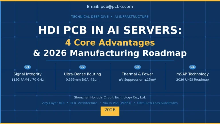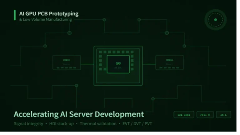
Why AI Server Backplanes Are Far More Complex Than Traditional Server Backplanes
AI server backplanes are architecturally distinct from traditional designs because they must concurrently manage terabit-scale throughput, sub-picosecond signal timing, and chassis-level power loads now routinely exceeding 15 kW. With current-generation accelerators surpassing 1,000 W per chip and 224G PAM4 in volume production, the AI server backplane has become the most electrically, thermally, and mechanically demanding PCB assembly in commercial infrastructure.
1. What Fundamentally Separates an AI Server Backplane from a Traditional Server Backplane?
Traditional server backplanes were engineered around 10G–25G NRZ signaling with insertion loss budgets of 20–25 dB at 12.5 GHz. A high-speed AI backplane operating at 224G PAM4 must sustain signal integrity at Nyquist frequencies above 56 GHz, compressing channel loss budgets below 35 dB across the full channel including connectors, vias, and trace routing. This is a 4× increase in Nyquist frequency that requires rethinking every stackup decision, via structure, and connector footprint from first principles.
By 2026, Tier 1 hyperscalers have completed first-wave compliance verification for 224G PAM4 in volume production. The industry’s attention has shifted from whether 3D EM simulation is necessary to harder second-order problems: via-to-via crosstalk at high routing density, spread-glass fabric mandates, HVLP3 copper foil specifications, press-fit connector discontinuity management, and cost-competitive high-yield manufacturing.
| Real-World Data Point Current-generation AI training nodes built around Blackwell-architecture GPUs (single-chip TDP exceeding 1,000 W–1,200 W) have pushed chassis-level power delivery well past 15 kW. This represents a 2× increase over H100-generation platforms and forces fundamental PDN architecture changes—including Vertical Power Delivery (VPD)—on the AI server backplane. |
| Authority Reference IEEE 802.3ck (2022) defines 100G-per-lane electrical requirements. OIF-CEI-112G-LR-PAM4 and the emerging OIF-CEI-224G specifications establish the channel compliance framework that AI server PCB design teams must now treat as mandatory baselines, not future targets. |
Golden Snippet: AI Server Backplane vs. Traditional Backplane — Core Specifications
| Parameter | Traditional Server Backplane | AI Server Backplane (2026 Node) |
| Max Lane Rate | 25G NRZ / 56G PAM4 | 112G PAM4 / 224G PAM4 |
| Nyquist Frequency | ~12.5 GHz | >56 GHz |
| Insertion Loss Budget | 20–25 dB @ 12.5 GHz | 30–35 dB @ 56 GHz |
| PCB Layer Count | 12–18 layers | 24–40+ layers (sequential lamination) |
| Copper Foil Spec | Standard ED, Rz 2–4 μm | HVLP3 or better, Rz ≤ 0.6 μm |
| Dielectric Material | FR4 / Megtron 6 | Megtron 7 / Tachyon 100G |
| Via Architecture | PTH with back-drill | PTH + back-drill OR buried/blind microvia (Anylayer/ELIC) |
| Connector Interface | Press-fit (fish-eye) | SMT high-speed + cable-backplane (Overpass) |
| Power Delivery (per chassis) | 1–3 kW | 10–20 kW (Blackwell-gen) |
| Power Architecture | 12 V ATX horizontal planes | 48 V ORv3 + Vertical Power Delivery (VPD) |
| Thermal Management | Forced air | DLC cold plates / immersion cooling |
| Design Cycle Time | 6–9 months | 12–24 months |
| Qualified Supplier Pool | Hundreds globally | ~15–20 globally |
2. Why Does 224G Backplane PCB Design Demand a Completely New Engineering Methodology?
At 224G PAM4, each SerDes lane operates at 112 Gbaud with four amplitude levels. Noise margins shrink to single-digit millivolts, and signal degradation mechanisms that were second-order effects at 56G PAM4 become first-order failure modes. Five distinct physical phenomena converge to make 224G backplane PCB design qualitatively different from all prior generations: via-to-via crosstalk, fiber weave effect, copper surface roughness, press-fit connector discontinuity, and via architecture transition.
2.1 Via-to-Via Crosstalk at High Routing Density
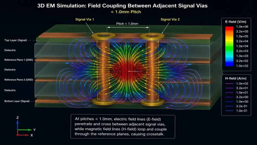
3D EM Simulation of Electromagnetic Field Coupling and Fringing Crosstalk Between Adjacent Signal Vias at < 1.0mm Pitch
As routing density increases to accommodate 128+ SerDes lanes per ASIC on the AI backplane PCB, via-to-via pitch tightens below 1.0 mm. At 56 GHz, electromagnetic coupling between adjacent via barrels—not trace-to-trace coupling—becomes the dominant crosstalk source. Required countermeasures include anti-pad shape optimization via 3D EM field solvers, ground via fence arrays at sub-0.8 mm pitch, and in the highest-density designs, migration to blind/buried microvia structures. None of these countermeasures have any equivalent in traditional high-speed server PCB design practice.
2.2 Fiber Weave Effect and Mandatory Spread Glass Fabric
At Nyquist frequencies above 56 GHz, the periodic variation in dielectric constant (Dk) between glass-bundle and resin-rich regions of standard woven glass fabrics (1067, 1080 weave) induces intra-pair skew of 4–8 ps/inch—sufficient to close PAM4 eye diagrams even with perfect trace length matching. This makes glass weave the dominant skew source at 224G, larger in magnitude than trace length mismatch. The mandatory engineering responses are: (1) specify spread glass fabric (1078S or 1086 weave) as a laminate requirement—not an option—to homogenize the dielectric cross-section, and (2) route differential pairs at 5°–15° to the primary glass axis (skewed routing). No combination of trace length tuning alone resolves fiber weave skew at 56 GHz Nyquist frequencies.
2.3 Copper Surface Roughness: HVLP3 as the 224G Minimum Standard
At 56 GHz Nyquist frequency, the skin depth of copper is approximately 0.28 μm. This means RF current is entirely confined to the outermost fraction of the conductor surface, making surface roughness a primary insertion loss mechanism. The specification of HVLP / UHVLP copper foil at Rz < 1.5 μm—appropriate for 112G PAM4—is insufficient for 224G. The current production standard for 224G AI backplane PCB is HVLP3 (Rz ≤ 0.6 μm) or equivalent ultra-low-profile foil. Critically, the surface treatment process must also be specified: conventional brown oxide (CuO) etching chemically roughens the copper surface and negates the roughness benefit of premium foil. Non-etching alternative oxide (alternative oxide or black oxide substitute) processes are mandatory when specifying HVLP3 foil for 224G AI server PCB design.
2.4 Press-Fit Connector Discontinuity and the Cable-Backplane Transition
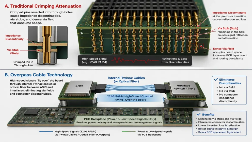
224G PAM4 AI Server Backplane: Overpass Cable Technology vs Traditional Press-Fit Connector
Traditional backplane interconnect relies on press-fit (fish-eye) connectors whose compliant pins are pressed into PTH vias. At 224G PAM4, each press-fit pin introduces a significant impedance discontinuity—caused by the annular ring geometry, the mechanical gap between pin and via barrel, and the via stub below the seating depth—that is extremely difficult to compensate through equalizer design alone. The industry response is a structural shift: SMT-terminated high-speed backplane connectors with controlled-impedance signal paths are replacing press-fit designs, and in the highest-performance configurations, direct cable-backplane (Overpass) architectures—where high-speed signals bypass the physical backplane PCB via active copper or optical cable assemblies—are eliminating the backplane via field entirely for the most demanding lanes. This architectural shift is one of the most commercially significant trends in AI server backplane design and has direct implications for PCB routing density, connector footprint design, and NRE investment strategy.
2.5 Back-Drilling Reality: Mechanical Limits and the Path to Advanced Via Architecture
The specification of residual stub ≤ 2 mil (0.05 mm) through mechanical back-drilling is technically achievable on thin-to-moderate thickness panels but becomes increasingly yield-destructive on 40-layer boards with total thickness of 6–8 mm. At these aspect ratios, cumulative registration tolerances from sequential lamination cycles, drill wander, and Z-axis depth control errors combine to push back-drilling yields below economically acceptable thresholds when targeting 2 mil residual stub across full panel area. The true engineering path forward is not to tighten mechanical back-drill specifications further, but to transition the via architecture: Laser Direct Imaging (LDI) combined with X-Ray Automated Optical Inspection (AOI) for registration verification, stepped via structures, or in the highest-density designs, full Anylayer or ELIC (Every Layer Interconnect) HDI architecture—where any-layer microvias replace through-hole structures entirely, eliminating the stub problem at its source rather than compensating for it.
| Engineering Reality — 2026 Production Status As of 2026, Tier 1 suppliers have completed 224G PAM4 compliance verification. The front line of engineering difficulty has shifted to: (1) via-to-via crosstalk in high-density 40-layer panels, (2) multi-lamination registration control for sequential lamination HDI builds, and (3) achieving commercial-viable yield on HVLP3 / non-etching surface treatment process combinations. Teams still optimizing mechanical back-drill depth as their primary 224G via strategy are one generation behind the current production baseline. |
224G Backplane PCB Design Challenge Matrix (2026 Edition)
| Challenge | Root Cause | Engineering Solution | 2026 Status |
| Via-to-via crosstalk | EM coupling between via barrels at < 1 mm pitch | Anti-pad tuning + GND via fence + microvia migration | Active engineering focus |
| Fiber weave skew | Non-uniform Dk from glass bundle / resin periodicity | Spread glass fabric (1078S/1086) + 5°–15° skewed routing | Mandatory at 224G |
| Copper conductor loss | Skin-effect current confined to Rz surface layer at 56 GHz | HVLP3 foil (Rz ≤ 0.6 μm) + non-etching surface treatment | 2026 production standard |
| Via stub resonance | PTH stub resonates at 56 GHz Nyquist | Back-drill < 2 mil OR transition to Anylayer / ELIC HDI | Back-drill: mature; HDI: leading edge |
| Press-fit discontinuity | Fish-eye pin geometry creates impedance discontinuity | SMT high-speed connectors + cable-backplane (Overpass) for critical lanes | Architectural transition underway |
| Multi-lamination registration | Sequential lamination shrinkage/expansion across 6–8 cycles | LDI registration + X-Ray AOI; Cpk ≥ 1.33 on layer-to-layer alignment | Key supplier differentiator |
| Dielectric loss | Df ≥ 0.009 exhausts channel budget before 4 inches | Megtron 7 (Df ≈ 0.0015) / Tachyon 100G (Df ≈ 0.0021) | Production standard |
| Immersion fluid / Dk drift | Fluorocarbon absorption shifts Dk/Df over deployment lifetime | Fluid-specific laminate qualification; +3–5 dB channel margin reserve | Emerging requirement |
3. How Does Power Delivery Architecture Differentiate AI Backplane PCB from All Prior Generations?
The power delivery challenge on an AI server backplane is not simply a matter of adding thicker copper. At the 15 kW+ chassis level demanded by current Blackwell-generation GPU nodes, two fundamental architectural limitations of horizontal (lateral) power distribution become critical failure modes: (1) unacceptable I²R losses on long horizontal power planes at 300–400 A bus currents, and (2) dynamic PDN collapse under high-di/dt transient loads generated by AI workload step changes.
3.1 Vertical Power Delivery (VPD) and Fractional Power Architecture (FPA)
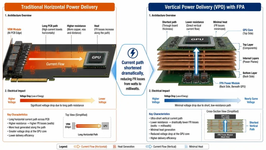
AI Server Backplane PDN Architecture Evolution — Traditional Horizontal Power Delivery vs. Vertical Power Delivery (VPD) with FPA
The industry response to horizontal PDN limitations at hyperscale AI densities is Vertical Power Delivery (VPD), in which power conversion stages are positioned physically adjacent to or directly above the load (GPU die) rather than distributed horizontally across the backplane. Combined with Fractional Power Architecture (FPA)—where 48 V is stepped down in multiple conversion stages across the board stackup—VPD reduces maximum lateral current on the AI backplane PCB by an order of magnitude, cutting I²R losses from watts to milliwatts on the critical delivery path. Any technical review of AI server backplane PDN complexity that treats copper thickening as the primary solution is describing architecture that Tier 1 hyperscalers have moved beyond.
3.2 High-di/dt Transient Response: The Dynamic PDN Challenge
AI training workloads generate load step transients—particularly during model-parallel synchronization events and optimizer steps—that transition from near-zero to full load in under 1 microsecond. The resulting di/dt can exceed 10 A/ns on the GPU power rail. A PDN designed only to meet steady-state ripple specifications (e.g., 1% at full load) will exhibit voltage undershoot excursions of 5–10% during transient events, potentially exceeding processor voltage guard bands and triggering throttling or hard resets. Managing dynamic PDN on an AI server backplane requires: target impedance profiling from 100 Hz to 1 GHz, staged bulk and high-frequency decoupling capacitor placement correlated to PDN simulation, and VRM loop bandwidth coordination—a discipline entirely absent from traditional server backplane engineering practice.
| Architectural Warning Specifying 3–6 oz copper planes as the primary solution to AI backplane power delivery is a legacy approach. At 400 A+ lateral bus currents, horizontal copper planes accumulate milliohm-range resistance producing voltage drops that exceed processor guard bands. Vertical Power Delivery (VPD) is the architecturally correct solution at current AI chassis power densities; copper thickening is a compensating measure, not a design strategy. |
PDN Architecture Comparison: Traditional vs. AI Server Backplane
| PDN Design Aspect | Traditional Server Backplane | AI Server Backplane (Current Gen) |
| Bus Voltage | 12 V ATX | 48 V / 54 V ORv3 |
| Peak Bus Current | < 50 A | 300–400 A+ |
| Power Distribution Model | Horizontal lateral planes | Vertical Power Delivery (VPD) + FPA |
| PDN Target Impedance | > 5 mΩ | < 0.5 mΩ (static) / < 1 mΩ (dynamic) |
| Transient Load Step (di/dt) | < 1 A/ns | ≥ 10 A/ns (AI step changes) |
| Dynamic Ripple Requirement | < 5% (relaxed) | < 1% steady-state; < 3% transient guard band |
| Copper Weight (power planes) | 1 oz (35 μm) | 3–6 oz, supplemented by VPD topology |
| OCP Compliance | Optional | DC-MHS / ORv3 mandatory |
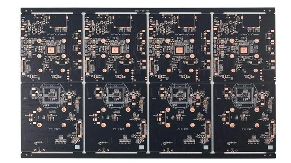
4. What Material, Fabrication, and HDI Process Advances Are Required for AI Backplane Manufacturing?
AI backplane PCB fabrication at the 224G node imposes laminate, copper foil, surface treatment, and sequential lamination process requirements that eliminate the majority of PCB manufacturers from consideration. Laminate material determines insertion loss per unit length; copper surface roughness determines the conductor loss contribution at 56 GHz; and multi-lamination registration control determines whether the via architecture required by 224G density is manufacturable at acceptable yield.
4.1 Sequential Lamination and Registration: The Manufacturer Qualification Gate
A 40-layer AI backplane PCB is not fabricated in a single press cycle. It requires 6–8 sequential lamination cycles, each introducing cumulative dimensional change (shrinkage and expansion) from thermal and pressure effects. The resulting layer-to-layer registration error compounds across cycles: a supplier achieving ±0.075 mm registration per cycle accumulates total misalignment that can misplace microvia landing pads and exceed impedance control tolerances by the final lamination cycle. This multi-lamination registration control—not raw layer count capability—is the manufacturing gate that screens out approximately 80% of globally active PCB fabricators from AI backplane PCB qualification. Laser Direct Imaging (LDI) for each inner layer and automated X-Ray registration verification between lamination cycles are minimum-standard process controls; suppliers without both are disqualified for 40-layer AI backplane programs regardless of other capabilities.
4.2 Advanced Via Architecture: Anylayer / ELIC HDI
For the highest routing density AI backplane PCB designs—particularly those accompanying Blackwell-architecture ASICs with 128+ SerDes lanes—conventional PTH via architecture reaches a physical limit. The transition path is to ELIC (Every Layer Interconnect) HDI or Anylayer microvia construction, in which filled copper microvias connect any layer pair, eliminating through-hole stubs entirely and enabling routing densities unreachable with PTH technology. The mSAP (Modified Semi-Additive Process) line/space capability (typically 25 μm / 25 μm) required for ELIC HDI further narrows the qualified supplier pool to fewer than 10 globally. Teams designing for this architecture must engage qualified suppliers at the initial design phase—not at tape-out—to co-develop DFM rules that are manufacturable at commercial yield.
4.3 Copper Foil and Surface Treatment: HVLP3 + Non-Etching Process
At 56 GHz Nyquist frequency, skin depth in copper is approximately 0.28 μm, confining RF current to the surface roughness profile. HVLP3 (Rz ≤ 0.6 μm) or equivalent ultra-low-profile foil is the 2026 production standard for 224G AI backplane PCB—not HVLP at Rz < 1.5 μm, which is appropriate only for 112G PAM4. Specifying premium low-roughness foil without controlling the surface treatment process is a common engineering error: standard brown oxide (CuO) treatments use alkaline etching chemistry that re-roughens the copper surface by 0.3–0.8 μm, negating the benefit of HVLP3 specification. Non-etching alternative oxide (proprietary non-etching adhesion promotion) processes are mandatory companion specifications for HVLP3 foil in volume AI server PCB design production.
4.4 Immersion Cooling and Laminate Long-Term Compatibility
Immersion cooling deployments expose laminates directly to dielectric fluids (fluorocarbon-based or synthetic ester). Long-term fluid absorption into laminate materials causes measurable Dk and Df drift that shifts channel impedance and degrades signal integrity over system lifecycle—a failure mode with no equivalent in air-cooled traditional server backplane deployments. For a 224G AI backplane PCB where channel margins are already within 3–5 dB of compliance limits at end-of-line test, a 5–10% Df increase from fluid absorption over 18–24 months of deployment can push channels below IEEE 802.3ck compliance thresholds without any physical failure event. Laminate qualification for immersion cooling must include fluid-specific absorption and electrical property drift data over 3,000+ hours of exposure—data not standardized in current IPC protocols and requiring direct supplier engagement.
| Fabrication Supply Chain Reality — 2026 The global pool of suppliers with verified capability for 40-layer+ AI backplane PCB production includes: TTM Technologies (US), Tripod Technology (TW), Shennan Circuits 深南电路 (CN), Unimicron 欣兴电子 (TW), and Nanya PCB 南亚电路板 (TW). For ELIC/Anylayer HDI AI backplane programs, the qualified pool narrows further to fewer than 10 globally. For programs requiring ultra-large-format panels or defense-grade reliability, US domestic specialty fabricators with ITAR-certified facilities require separate evaluation. First prototype spin yields for 40-layer Megtron 7 builds commonly fall below 60%; HVLP3 + non-etching process qualification adds 4–6 weeks to qualification timeline. |
Laminate Selection Guide — Calibrated Cost Model (FR4 Baseline = 1×)
| Material | Df @ 10 GHz | Max Lane Rate | Cost vs. FR4 (1×) | Cost vs. Megtron 6 | Use Case |
| FR4 (standard) | 0.020 | ≤ 10G NRZ | 1× (baseline) | — | Traditional server backplane |
| Isola FR408HR | 0.009 | 25G NRZ / 56G PAM4 | ~2× | ~0.6× | Transitional designs |
| Megtron 6 | 0.002 | 112G PAM4 | ~3.5× | 1× (ref.) | High-speed AI server PCB design |
| Megtron 7 | 0.0015 | 224G PAM4 | ~5× | ~1.4× | Current 224G AI backplane standard |
| Tachyon 100G | 0.0021 | 112G–224G PAM4 | ~4.5× | ~1.3× | Megtron 7 alternative |
| Rogers 3003 | 0.0013 | 224G (critical segments) | 7×+ | ~2× | Highest-performance segments only |
| Cost Baseline Note All multipliers use FR4-based traditional server backplane as the universal 1× baseline. Total fabricated panel cost for a 40-layer Megtron 7 AI backplane PCB—including laminate premium, back-drilling or microvia process operations, IPC Class 3/A inspection, and yield-loss amortization across 2–4 prototype spins—reaches 6×–8× the equivalent FR4 traditional backplane panel. This figure is self-consistent: the 5× laminate material premium plus fabrication process premium plus yield-loss factor produces the 6×–8× total, not a contradiction with per-material comparisons. |
5. How Do Thermal, Mechanical, and Reliability Constraints Compound AI Server PCB Design Complexity?
High-layer-count AI backplane PCBs face a structural paradox: the thicker copper planes and higher layer counts required for power delivery increase board thickness to 6–8 mm, raising via aspect ratios and requiring the advanced via architectures described in Section 2 and Section 4. Simultaneously, the thermal management technologies required to manage 15 kW+ chassis power introduce new mechanical and chemical stress pathways that are absent from traditional server backplane reliability models.
5.1 PTH Barrel Cracking and Microvia Reliability Under Thermal and Mechanical Stress
IPC reliability data for 40+ layer AI backplane PCBs operating at 85°C board temperatures shows significantly elevated PTH barrel crack rates after 1,000 thermal cycles (−40°C to +125°C) versus 16-layer traditional designs, driven by CTE mismatch at the laminate-copper interface. DLC cold plate assemblies impose additional cyclic mechanical clamping stress that compounds this failure mode. The industry response is IPC Class 3/A acceptance criteria with ≥ 25 μm copper wrap plating on all PTH barrels, 100% electrical test, and in the highest-reliability designs, migration of critical signal vias to blind/buried microvia structures that are inherently immune to barrel cracking—while being aware that filled microvia stacking reliability under thermal cycling requires its own qualification regime.
5.2 Immersion Cooling: Long-Term Dielectric and Mechanical Degradation
Immersion cooling introduces two AI-backplane-specific failure modes. First, DLC cold plate mechanical clamping stress on 6–8 mm boards accelerates PTH barrel micro-cracking through cyclic compression—a failure mechanism absent from air-cooled designs. Second, fluorocarbon and synthetic ester dielectric fluids used in single-phase and two-phase immersion systems cause progressive Dk and Df drift in Megtron-class laminates. For 224G AI backplane PCBs where channel insertion loss margins are already near compliance limits, a 5–10% Df increase from fluid absorption mid-deployment can push channels out of IEEE 802.3ck compliance without any visible physical damage. Design teams must build 3–5 dB of additional insertion loss margin into channel budgets for immersion-cooled deployments and require 3,000-hour fluid absorption and electrical property drift certification from laminate suppliers before material selection.
| Reliability Standard Leading AI backplane PCB suppliers specify IPC Class 3/A as the minimum acceptable tier, with copper wrap plating ≥ 25 μm, 100% electrical test, filled and capped microvias, and back-drill residual stub ≤ 2 mil. For Anylayer/ELIC HDI builds, stacked microvia shear testing under thermal cycling is an additional mandatory qualification. These requirements add 15–20% to fabrication cost but are necessary to achieve field failure rates below 0.1% DPPM at hyperscale deployment volumes. |
6. How Should Engineering and Procurement Teams Evaluate AI Server Backplane PCB Suppliers?
Selecting a fabrication or design partner for an AI backplane PCB requires verifying capabilities that do not appear on standard vendor qualification checklists. The following evaluation matrix reflects 2026 production requirements for 224G-capable AI server backplane programs.
| Evaluation Criterion | Minimum Requirement | Disqualifying Signal |
| Layer count / thickness | 40+ layers, 6–8 mm board thickness | No production record above 32 layers |
| Sequential lamination registration | LDI per inner layer + X-Ray AOI; Cpk ≥ 1.33 on layer-to-layer alignment | Registration specified only as ±0.1 mm or no Cpk data |
| Advanced via capability | PTH back-drill to ±0.05 mm (2 mil) AND/OR Anylayer/ELIC HDI qualification | Only standard PTH; no microvia qualification |
| Copper foil & surface treatment | HVLP3 (Rz ≤ 0.6 μm) process-qualified with non-etching alternative oxide | HVLP (Rz 1.0–1.5 μm) as highest spec; standard brown oxide only |
| Spread glass fabric process | 1078S / 1086 qualified build process | Only 1067/1080 standard weave available |
| Laminate qualification | Megtron 7 or Tachyon 100G process-qualified | FR4/FR408HR as highest qualified material |
| Immersion cooling compatibility | Fluid absorption / Dk-Df drift certification data available | No laminate-fluid interaction testing |
| SI simulation support | In-house 3D EM (Ansys HFSS / CST) + hardware S-parameter correlation | Relies solely on 2D transmission line models |
| 224G compliance test | VNA to 110 GHz + PAM4 BERT | No 56 GHz+ test equipment |
| Connector support | SMT high-speed backplane connector + cable-backplane (Overpass) experience | Press-fit PTH only; no SMT/cable-backplane reference design |
| PTH reliability standard | IPC Class 3/A; copper wrap ≥ 25 μm; microvia option for critical nets | IPC Class 2 as highest standard |
| Reference customer tier | Tier 1 hyperscaler or AI infrastructure OEM | Enterprise-only or telecom-only references |
Early DFM Engagement: The Highest-ROI Action in Any AI Backplane PCB Program
A structural feature of AI backplane PCB programs that is absent from traditional server backplane development is the outsized impact of early supplier engagement on total program cost. Given first prototype spin yields commonly below 60% on 40-layer Megtron 7 builds, and 2–4 prototype iterations as a typical qualification path, the NRE cost differential between a program that engages a qualified supplier with 224G simulation capability at initial schematic stage versus at tape-out is $300K–$800K in avoidable prototype respins.
A qualified AI backplane PCB partner engaged at the Design-in Phase—before stackup is finalized, before via structures are committed, and before connector footprints are locked—can provide DFM review that eliminates via crosstalk issues, identifies spread glass fabric conflicts with the chosen routing angle, and flags HVLP3 / surface treatment compatibility issues before they become silicon-facing yield problems. This early co-development model is standard practice among Tier 1 hyperscalers and is increasingly being adopted by AI infrastructure OEMs as a supply chain risk mitigation requirement.
| Supplier Landscape — 2026 The global pool for 40-layer+ volume AI backplane PCB: TTM Technologies (US), Tripod Technology (TW), Shennan Circuits 深南电路 (CN), Unimicron 欣兴电子 (TW), Nanya PCB 南亚电路板 (TW). For ELIC/Anylayer HDI AI backplane programs, the qualified pool narrows to fewer than 10 globally. US domestic specialty fabricators with ITAR certification serve defense/aerospace AI infrastructure programs. Engage qualification 12–18 months before production target date. |
The industry’s dirty secret in 2026 is that nobody actually wants to build a pure 40-layer mechanical back-drilled PTH board at 224G; teams are either forced into early, cost-prohibitive Overpass cable architectures or betting the entire program on sequential-lamination ELIC HDI with strategic vendor co-development.
FAQ: AI Server Backplane Engineering
How to reduce via crosstalk in 224G PCB design — what are the specific countermeasures?
Via-to-via crosstalk in 224G AI backplane PCB design is a 3D electromagnetic problem that 2D trace routing rules cannot address. The required countermeasures, in order of effectiveness, are: (1) Anti-pad shape optimization using 3D EM field solvers (Ansys HFSS or CST Studio Suite)—circular anti-pads are replaced with tuned elliptical or cross-shaped geometries that minimize electric field coupling between adjacent barrels at 56 GHz. (2) Ground via fence arrays at ≤ 0.8 mm pitch around every differential signal via pair, tied to continuous ground planes on all layers. (3) Via pitch relief—where routing density permits, increasing signal via pitch from 0.8 mm to 1.0 mm reduces crosstalk by 6–10 dB. (4) For the highest-density sections, migration to blind/buried microvia or Anylayer ELIC architecture eliminates the through-hole barrel entirely, removing the crosstalk source. Mechanical back-drilling does not reduce via-to-via crosstalk; it only addresses stub resonance.
Megtron 7 vs. Tachyon 100G insertion loss at 56 GHz — how do they compare in practice?
Both Megtron 7 and Tachyon 100G are production-qualified materials for 224G AI backplane PCB, but they differ in three practically significant ways. Insertion loss: Megtron 7 (Df ≈ 0.0015 at 10 GHz) provides approximately 10–12% lower dielectric loss than Tachyon 100G (Df ≈ 0.0021 at 10 GHz) across equivalent trace lengths at 56 GHz Nyquist—a meaningful margin advantage in tight channel budgets. Process compatibility: Tachyon 100G has broader PCB fabricator qualification at standard-tier suppliers; Megtron 7 is more consistently processed by Tier 1 facilities with dedicated Panasonic laminate process controls. Cost: Megtron 7 carries an approximately 10–15% material cost premium over Tachyon 100G at equivalent build specifications. In practice, Megtron 7 is preferred for channel-budget-constrained designs where every dB of insertion loss margin matters; Tachyon 100G is a viable alternative where supplier flexibility or cost reduction is a priority. Both require HVLP3 copper foil and non-etching surface treatment to realize their full loss performance at 56 GHz.
What are IPC Class 3/A back-drilling tolerances, and why does the 2 mil spec fail on thick AI backplane panels?
IPC-6012 Class 3/A establishes the highest commercial reliability acceptance criteria for PCB fabrication. For back-drilling, it specifies residual stub length as a critical process control parameter—a 2 mil (0.05 mm) residual stub is the specification most commonly cited for 224G AI backplane PCB. This specification is achievable and production-stable on panels up to approximately 3.2 mm (approximately 24–28 layers). On 40-layer AI backplane PCBs with total thickness of 6–8 mm, the combination of drill wander at high aspect ratios, Z-axis depth control variation, and cumulative registration error from sequential lamination makes 2 mil residual stub specification across full panel area yield-destructive at volume production scale. The engineering resolution is not to relax the electrical specification but to change the via architecture: transition to blind vias, buried vias, or Anylayer ELIC HDI structures that eliminate the stub entirely, rather than attempting to back-drill to increasingly aggressive depths on progressively thicker substrates. Suppliers who present 2 mil back-drill specification for 40-layer AI backplane programs without qualification data showing Cpk ≥ 1.33 on stub depth across production panels should be treated as unqualified for that specification.
When should an AI server backplane design transition from press-fit connectors to SMT or cable-backplane (Overpass) architecture?
The transition threshold from press-fit to SMT or cable-backplane architecture is driven by two independent factors: lane rate and lane count. On lane rate: press-fit connector discontinuity becomes a signal integrity first-order problem at 112G PAM4 and above. The impedance discontinuity introduced by the compliant pin-to-barrel interface and the via stub below the seating depth is large enough at 56 GHz Nyquist to require aggressive equalization that consumes a significant portion of the available SerDes power budget, and becomes unmanageable for 224G PAM4 without architectural change. On lane count: when an AI server backplane carries more than 64–96 high-speed differential lanes at 112G+ rates, the via field density required for press-fit connector footprints consumes routing space that would otherwise be available for via crosstalk mitigation structures. The cable-backplane (Overpass) architecture—in which the physical backplane PCB carries power, control, and lower-speed signals while high-speed AI data lanes are routed via direct-attach active copper or optical cable assemblies—is now the preferred architecture for the most demanding AI server backplane applications. It eliminates connector discontinuity and via field crosstalk simultaneously, at the cost of increased system integration complexity and cable management overhead.
How does early DFM engagement with a 224G-capable PCB supplier reduce AI backplane program NRE cost?
The NRE cost structure of an AI server backplane PCB program is heavily front-loaded: a single 40-layer Megtron 7 prototype panel with HVLP3 copper, controlled back-drilling, and IPC Class 3/A inspection costs $25K–$60K per spin, with typical first-spin yields below 60%. A program that reaches tape-out before engaging a qualified supplier for DFM review will commonly encounter 2–3 avoidable respins driven by: via crosstalk issues that 2D simulation did not predict (requiring via pitch relief or architecture change), fiber weave conflicts with the routing angle (requiring re-routing or spread glass fabric substitution), and HVLP3 / surface treatment process incompatibilities at the selected fabricator (requiring supplier requalification). Engaging a PCB manufacturing partner with demonstrated 224G AI backplane PCB simulation capability at the initial Design-in Phase—before stackup finalization, via structure commitment, and connector footprint lock—eliminates these respins through concurrent DFM review. The financial impact is $300K–$800K in avoidable prototype costs and 3–6 months of schedule recovery, against an early engagement cost that is typically zero for qualified Tier 1 suppliers seeking strategic design wins.
Using top-tier AI server PCB equipment to manufacture traditional PCBs delivers a strategic advantage: interlayer alignment tolerance shrinks from ±75μm to within ±25μm, and differential impedance control tightens to ±5%. Paired with 100% 3D X-Ray inspection, it grants conventional boards chip-level precision, superb signal stability, and near-100% yield.
Still, need help? Contact Us: sales@pcbkr.com
Need a PCB or PCBA quote? Quote now
About Author
David Chen https://www.linkedin.com/in/pcbcoming
David Chen boasts an extensive professional background in PCBA manufacturing, PCBA testing, and PCBA optimization, with specialized expertise in high-precision PCBA fault analysis and rigorous PCBA reliability testing. Skilled in complex circuit design and cutting-edge advanced PCB manufacturing processes, he delivers solutions that elevate product durability and performance across industrial applications. His technical articles focusing on PCBA manufacturing workflows and testing methodologies are widely cited by industry peers, research institutions, and technical platforms, solidifying his reputation as a recognized technical authority in the global circuit board manufacturing sector.