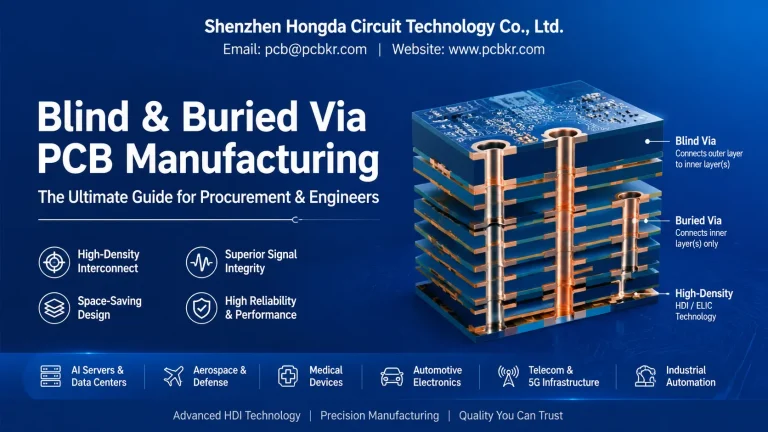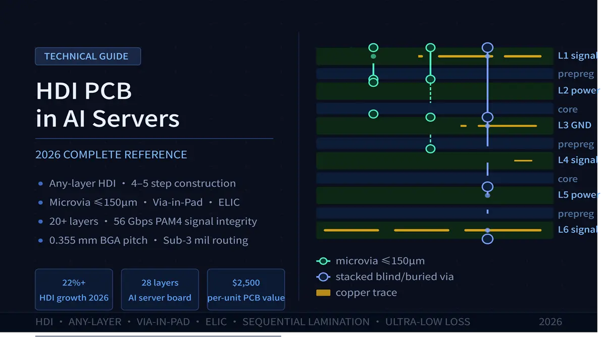
HDI PCB in AI Servers: The Complete Technical Guide (2026)
Introduction
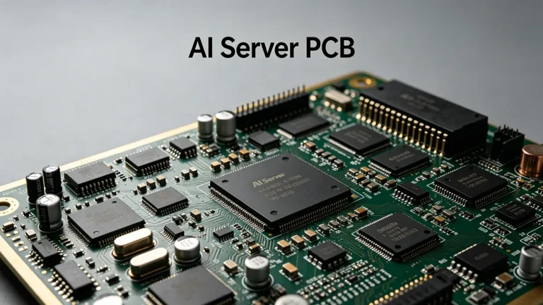
The rapid proliferation of AI infrastructure has fundamentally transformed the demands placed on printed circuit board technology. As AI servers grow denser, faster, and more thermally challenging, High-Density Interconnect (HDI) PCBs have emerged as the foundational enabling technology — not a premium option, but an absolute requirement. A single AI server motherboard can incorporate $1,000–$2,000 worth of PCB value, and that figure is rising. This guide covers everything hardware engineers, procurement teams, and OEM/EMS manufacturers need to know about HDI PCB design, manufacturing, and selection for AI server applications.
Why AI Servers Need HDI PCBs: 4 Core Drivers
Traditional server PCB architectures were designed for a world of comparatively modest compute density. Modern AI accelerators have broken every assumption that world rested on. Four distinct forces are driving the shift to HDI:
HDI PCB in AI Servers High-Density Interconnect Requirements
Today’s GPU and CPU packages feature BGA pitches as tight as 0.4 mm, with advanced HBM memory routing demanding 0.355 mm pitch precision. Standard through-hole via technology simply cannot route these packages without catastrophic signal congestion. Any-layer HDI construction, combined with via-in-pad techniques and laser-drilled microvias, enables the routing density required. AI accelerator boards routinely carry $1,000–$2,000 in PCB value precisely because of the complexity this demands.
HDI PCB in AI Servers High-Speed Signal Transmission
PCIe 5.0 and 6.0 interfaces, 56 Gbps PAM4 signaling, and emerging 112G transmission rates impose stringent signal integrity requirements that conventional PCB construction cannot satisfy. Microvias reduce signal loss by more than 30% compared to through-hole vias of equivalent function and measurably reduce cross-delay. These gains are not marginal — at 56 Gbps and beyond, they determine whether a design passes or fails compliance testing. The market has responded: HDI PCB shipments grew 17.8% in 2024, making it the fastest-growing PCB category that year.
HDI PCB in AI Servers Multi-Layer Design Requirements
Modern AI server motherboards require 18–22 layers of interconnect; GPU substrates are moving toward 20+ layers, with 2026 designs projected to reach 22–28 layers. Any-layer HDI construction with hybrid stacking is the only practical way to achieve this layer count while maintaining routing integrity and manageable board thickness. For context, 18+ layer PCBs already command a price premium roughly three times that of 12–16 layer equivalents.
HDI PCB in AI Servers Thermal Management and Power Density
Local power densities exceeding 100 W/cm² generate thermal gradients that conventional materials cannot tolerate. HDI construction addresses this through filled-via electroplating, which improves thermal conductance through the stack, and through the use of High-Tg (HTg) dielectric materials with better CTE matching. Optimized power routing in HDI designs enables power supply ripple to remain below the 20 mV peak-to-peak threshold that AI accelerators require for stable operation.
Six Key Application Scenarios for HDI PCBs in AI Servers
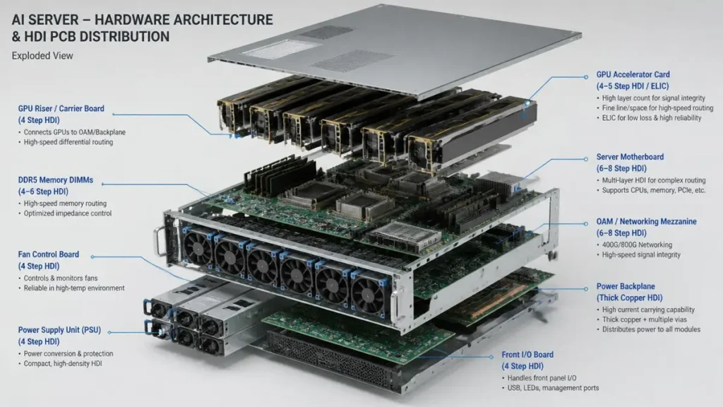
AI SERVER – HARDWARE ARCHITECTURE & HDI PCB DISTRIBUTION
HDI is not a single monolithic technology — it encompasses a family of constructions matched to specific application needs within the AI server ecosystem.
AI Server Motherboards
The central integration hub of any AI server, the motherboard must orchestrate dozens of high-speed interfaces between CPUs, GPUs, memory, and I/O controllers. Hybrid HDI combined with conventional multilayer construction, targeting 20–22 layers of any-layer HDI, delivers the signal integrity required. Sequential lamination and laser drilling are the defining manufacturing processes. NVIDIA’s Blackwell GB200 architecture exemplifies the complexity this scenario demands.
GPU Accelerator Card Substrates
GPU accelerator cards represent the highest-complexity HDI application in the AI server stack. Designs require 4–5 step HDI construction across 16–20 total layers, utilizing via-in-pad, ELIC (Embedded Light Interconnect Construction), and sub-3 mil routing throughout. The NVIDIA H100 and B100 accelerator card families are representative products in this category.
CPU Substrates
CPU substrate designs for AMD EPYC and Intel Xeon platforms require Type 3 HDI construction across 18–20 layers. Blind and buried via technology with staggered via stacking delivers the routing density for modern multi-chip CPU packages.
HBM Memory Carriers
HBM3 and HBM3e memory modules depend on any-layer HDI with microvias across 12–16 layers. The defining technical challenge is routing 0.355 mm BGA pitch connections between the memory stack and its carrier substrate — a task that demands the finest geometries in production HDI manufacturing.
Power Backplanes
AI server power management systems require high-layer HDI construction across 14–18 layers. Thick copper construction combined with low-loss dielectric materials enables the current-carrying capacity and thermal stability that hundred-kilowatt AI server racks demand.
Network Cards and Riser Cards
PCIe 5.0 network interface cards and riser cards operate at the lower end of the HDI complexity spectrum, typically requiring Type 2 HDI across 10–14 layers. Impedance control and EMI suppression are the governing design constraints.
HDI PCB Technical Specifications in NVIDIA AI Servers
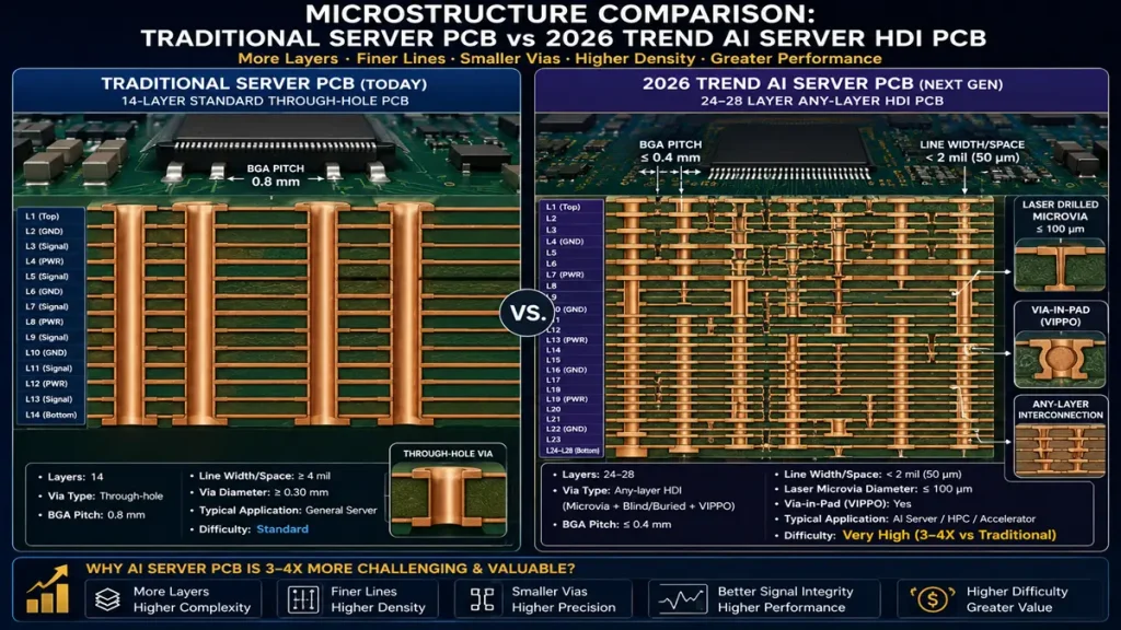
Microstructure Cross-Section Comparison: Traditional Through-Hole Server PCB vs. 2026 Trend High-Density Interconnect (HDI) AI Server PCB.
The evolution from 2019-era traditional servers to today’s AI server generation represents a discontinuous jump in PCB complexity — not incremental improvement.
| Specification | 2019 Traditional Server | 2024 AI Server | 2026 Trend |
|---|---|---|---|
| Motherboard Layer Count | 14 layers | 18–22 layers | 22–28 layers |
| GPU Substrate Layer Count | 12–14 layers | 20+ layers | 24–28 layers |
| HDI Step Count | 1–2 steps | 4–5 steps | 5–6 steps (UHDI) |
| BGA Pitch | 0.8 mm | 0.4 mm | 0.355 mm |
| Line Width/Space | 5–6 mil | 3 mil | Below 2 mil |
| Microvia Diameter | 200 μm (mechanical drill) | ≤150 μm (laser drill) | ≤100 μm |
The transition from mechanical to laser drilling is particularly consequential. Mechanical drilling cannot reliably achieve diameters below 200 μm, and the aspect ratio limitations of mechanical drilling impose hard constraints on layer counts. Laser drilling at ≤150 μm, with a roadmap toward ≤100 μm, unlocks the via density that 20+ layer AI server designs require.
Key HDI Manufacturing Processes in AI Server PCBs
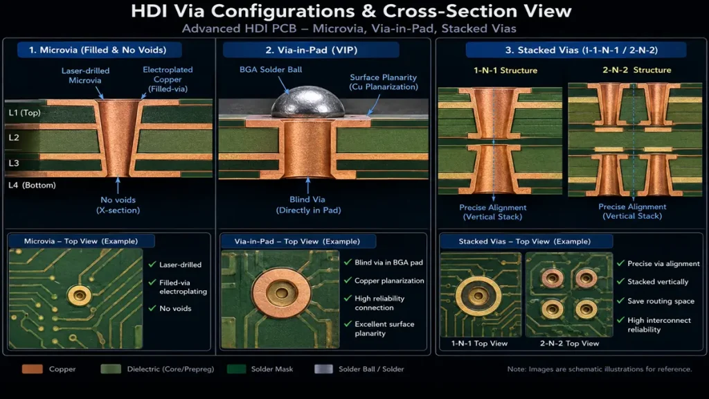
Advanced HDI Via Configurations & Cross-Section View: Engineering Analysis of Microvia, Via-in-Pad (VIP), and Vertically Stacked Vias (1-N-1 & 2-N-2).
Six manufacturing processes define the HDI capability set that AI server designs demand. Understanding them is essential for both design engineers and procurement teams evaluating supplier capability.
Microvias
Laser-drilled holes with diameters at or below 150 μm and depths no greater than 0.15 mm constitute the fundamental building block of HDI. In AI server applications, microvias reduce signal loss by more than 30% relative to through-hole alternatives and provide the via density that dense BGA routing requires. Manufacturing precision demands via alignment accuracy within 50 μm and complete filled-via electroplating without voids.
Via-in-Pad
Placing vias directly within BGA landing pads, then filling and plating them flat, eliminates the dogbone escape routing that conventional PCB design requires. The result is approximately 40% space savings and meaningfully shorter signal paths. The manufacturing challenge lies in maintaining surface planarity and keeping void content below 5% — voids create solder reliability problems during reflow.
Sequential Lamination
The process of building up layers in 2–5 layer increments, laser drilling, then pressing again — repeated 4–5 times for the most complex AI server designs — is what enables 4–5 step HDI and 20+ total layer counts. The manufacturing risks are layer-to-layer alignment and the cumulative thermal stress that multiple lamination cycles impose on the dielectric stack.
ELIC (Embedded Light Interconnect Construction)
ELIC embeds the finest interconnect structures within the core of the PCB stack, enabling sub-3 mil routing geometries that are required for 0.355 mm BGA pitch. This is currently the most demanding production process in commercial HDI manufacturing, requiring line width control at sub-3 mil precision and tight resistance management across embedded traces.
Stacked Blind/Buried Vias
Via-in-via stacking in 1-N-1 and 2-N-2 configurations reduces total layer requirements by approximately 15% for a given routing density, translating directly to cost reduction. Successful execution requires complete via fill integrity across all stacked levels — partial fill creates reliability risks under thermal cycling.
Ultra-Low Loss Materials
Signal integrity at 56 Gbps and above demands dielectric materials with insertion loss below 0.04 dB/inch at 10 GHz and CTE values matched to the copper and via fill materials. The manufacturing challenge is maintaining consistent material properties — CTI values and adhesion strength — across production panels and across thermal cycling exposure.
AI Server HDI PCB Market Trends and Cost Data (2026)
The market data tells a compelling story about where value is concentrating in the AI server supply chain.
| Metric | 2023 | 2024 | 2026 Forecast |
|---|---|---|---|
| Global AI Server Shipment Growth | 50% | 80%+ | 100%+ |
| HDI PCB Year-over-Year Growth | 12% | 17.8% | 22%+ |
| High-End HDI Demand Growth | 80% | 150% | 200%+ |
| AI Server PCB Value vs. Traditional | 3× | 3× | 4× |
| Per-Unit PCB Cost | $800–$1,200 | $1,000–$2,000 | $1,500–$2,500 |
| 18+ Layer PCB Price Premium | 2.5× | 3× | 3.5× |
| AI Server PCB vs. Consumer Electronics | 8× | 12× | 15× |
Several dynamics in this data deserve attention. The per-unit PCB value in AI servers has already crossed $2,000 at the high end, a figure that would have seemed implausible for a circuit board five years ago. The 12× premium over consumer electronics PCBs reflects not just material and process costs but also the supply chain concentration in advanced HDI manufacturing — relatively few facilities worldwide can reliably produce 20+ layer, 4–5 step HDI at volume. That supply concentration is a sourcing risk that procurement teams must actively manage.
The 17.8% growth rate for HDI PCBs in 2024 — the fastest of any PCB category — reflects AI infrastructure investment flowing directly into advanced PCB demand. As AI server shipments are projected to continue growing at 80–100%+ annually, the pressure on HDI manufacturing capacity will intensify.
Five Technical Challenges and HDI Solutions in AI Server PCBs
AI server PCB design involves a cluster of interrelated technical challenges. HDI construction addresses each, but the solutions introduce their own manufacturing constraints that must be managed.
Signal Integrity Degradation
At 56 Gbps and above, through-hole vias become significant signal degradation sources due to stub effects and dielectric losses. Microvia replacement of through-hole vias reduces loss by more than 30% and cross-delay by approximately 40%. Managing this challenge requires simulation-driven design with full via field modeling, not rule-of-thumb design practices.
Power Supply Ripple
GPU instability and unexpected resets are frequently traceable to power supply ripple exceeding the 20 mV peak-to-peak threshold. HDI’s optimized power routing, combined with HTg materials and careful decoupling capacitor placement in via-in-pad configurations, achieves ripple stability improvement of approximately 50% compared to conventional construction. The gain comes from shorter current paths and better-controlled impedance in the power distribution network.
Thermal Stress-Induced Microvia Failure
The thermal cycling that AI servers undergo — from cold startup to full-load operation — creates CTE-driven stress concentrations at microvia interfaces. Filled-via electroplating with CTE-matched materials, validated through thermal cycling qualification to more than 1,000 cycles, is the established solution. Designs that skip fill electroplating on cost grounds frequently encounter field reliability problems.
0.355 mm BGA Routing Feasibility
Routing a 0.355 mm pitch BGA escape on a conventional PCB is geometrically impossible above a small number of signal layers. ELIC construction with sub-3 mil routing geometries and any-layer HDI escape routing achieves routing success rates above 95% on compliant designs. This is a binary capability requirement — suppliers without sub-3 mil production capability simply cannot produce these boards.
Layer-to-Layer Alignment in 20+ Layer Stacks
As layer counts increase, cumulative registration error across sequential lamination cycles can produce via misalignment that causes open circuits or reliability failures. Laser drilling with alignment accuracy within 50 μm, combined with automated optical inspection after each lamination cycle, achieves layer alignment rates of 98%+ in mature manufacturing processes.
Five Evaluation Criteria for AI Server HDI PCB Manufacturers
Selecting an HDI PCB supplier for AI server applications is a high-stakes decision. The following framework covers the five dimensions that matter most.
Layer Count Capability
A supplier’s maximum production layer count sets the ceiling on what designs they can support. For AI server applications, suppliers should demonstrate production capability at 28 layers or above, with documented yields, not just theoretical claims. Request design-for-manufacturing (DFM) review capability and validated sample data at target layer counts.
HDI Precision
Microvia diameter capability and maximum step count define a supplier’s HDI sophistication. AI server roadmaps require microvia diameters at or below 100 μm and 5–6 step UHDI capability for leading-edge designs. Verify through microscopy inspection and X-ray cross-section of qualification coupons — specification sheets alone are insufficient.
First-Pass Yield
Production yield at 95% or above is the threshold for economically viable AI server PCB sourcing. Below this level, schedule risk and landed cost become unmanageable. Request batch-level statistical yield data and third-party inspection reports rather than supplier-reported averages.
Material Certifications
UL94-V0 flammability rating, IPC-6012 Class 3 qualification, and ISO 9001 certification are baseline requirements. For high-speed signal applications, verify material-level data on insertion loss, Dk/Df at operating frequencies, and CTE values — not just that a named material is used, but that incoming material is tested against specification.
Lead Time and Capacity
Standard 15-day and expedited 7-day lead times are reasonable benchmarks for production-ready AI server HDI designs. Verify capacity claims through order tracking records and documented production capacity certificates. In a constrained HDI supply market, paper capacity commitments have limited value
HDI PCB technology is not a feature of AI servers — it is a prerequisite. As GPU pitches tighten to 0.355 mm, signal speeds cross 56 Gbps, and layer counts push past 20, the gap between HDI-capable and HDI-limited suppliers will determine which manufacturers can participate in the AI infrastructure buildout. For hardware engineers, understanding the six key processes — microvias, via-in-pad, sequential lamination, ELIC, stacked vias, and ultra-low-loss materials — is essential for design success. For procurement teams, the five evaluation criteria above provide a structured framework for qualifying suppliers before committing to a program.
The market data is clear: AI server PCB value is rising, HDI demand is accelerating faster than any other PCB category, and the cost of field failures in production AI infrastructure is severe. Investment in rigorous HDI supplier qualification is not overhead — it is risk management for one of the highest-stakes manufacturing decisions in the AI hardware supply chain.
Find Out About Us: Delivering Top-Tier Fabrication for Both AI & Conventional PCBs
Navigating the line between cutting-edge innovation and high-volume, cost-effective production shouldn’t be a compromise. At Shenzhen Hongda Circuit Technology (PCBKR), we bridge this gap by elevating the manufacturing standards for both high-performance AI hardware and traditional multi-layer PCBs.
By integrating advanced manufacturing methodologies across all production lines, we bring an elite level of precision to traditional PCB fabrication. Our standard boards benefit from enhanced interlayer alignment tolerances (down from ±75μm to within ±25μm) and tightened differential impedance control (±5%). Supported by 100% 3D X-Ray (AXI) inspection, your conventional boards achieve chip-level reliability, superb signal stability, and near-100% yield.
Your Strategic Manufacturing Partner
We proudly stand as a dual-capability partner: offering the elite technical ceiling required for next-gen AI hardware, while maintaining the exceptional flexibility, rapid turnaround, and unmatched cost-efficiency needed for mid-to-high-volume traditional board campaigns. You get zero-defect reliability without the premium overhead or bureaucracy of massive tier-1 factories.
Ready to upgrade your hardware’s reliability?
Submit your Gerber files today for an agile engineering review and a highly competitive quote.
Contact our experts: sales@pcbkr.com
About Author
David Chen https://www.linkedin.com/in/pcbcoming
David Chen boasts an extensive professional background in PCBA manufacturing, PCBA testing, and PCBA optimization, with specialized expertise in high-precision PCBA fault analysis and rigorous PCBA reliability testing. The author has worked with high-layer-count server PCB fabrication, ultra-low-loss backplane stackups, and thermo-mechanical reliability optimization for AI infrastructure projects involving 112G and 224G PAM4 architectures. Skilled in complex circuit design and cutting-edge advanced PCB manufacturing processes, he delivers solutions that elevate product durability and performance across industrial applications. His technical articles focusing on PCBA manufacturing workflows and testing methodologies are widely cited by industry peers, research institutions, and technical platforms, solidifying his reputation as a recognized technical authority in the global circuit board manufacturing sector.