mSAP Process vs Subtractive Etching in HDI Fabrication:
A Technical Comparison for Any-Layer HDI PCB Capabilities, IC Substrates, and Advanced Interconnect Design
Published by Shenzhen Hongda Circuit Technology Co., Ltd. | 2026 | Technical Series
Executive Summary: Why mSAP Is Redefining PCB Manufacturing in 2026
Shenzhen Hongda Circuit Technology Co., Ltd. has commissioned its dedicated mSAP production line, achieving verified mass-production capability at 30/30 µm line/space (L/S) with a qualification roadmap extending to 20/20 µm — equivalent to 1.2/1.2 mil — for substrate-like PCB (SLP) and IC carrier applications. This white paper provides a detailed engineering comparison of the mSAP process versus conventional subtractive etching across all relevant parameters: achievable trace geometry, impedance consistency, copper utilization, layer-to-layer registration, and production yield.
For engineering decision-makers evaluating PCB suppliers for AI accelerators, advanced mobile SoC packages, System-in-Package (SiP) modules, or any-layer HDI interconnect designs, this document supplies the quantified data needed to make an informed sourcing choice.
Technology Drivers: Why the PCB Industry Had to Move Beyond Subtractive Etching
1. The Density Inflection Point in Advanced Electronics
Three converging forces have pushed mainstream PCB fabrication beyond what subtractive copper etching can reliably deliver:
- AI accelerator boards (GPUs, NPUs, and custom ASICs) now require PCBs that function as extensions of the semiconductor package, with fine-pitch BGA escapes demanding sub-40 µm trace resolution.
- 5G/6G mmWave RF front-ends require tightly controlled impedance (±5% or better) across differential pairs routed in dense HDI stacks — tolerances subtractive etching cannot guarantee at fine pitch.
- SiP integration places multiple bare dies on a single substrate, compressing board area while demanding simultaneous signal integrity, power delivery, and thermal management on a layer count of 10–20+.
Subtractive processes — even in their most refined HDI forms — are fundamentally limited by copper undercut during etching. As trace widths drop below 40 µm, the isotropic chemical etch removes copper laterally at almost the same rate it removes it vertically, producing trapezoidal trace cross-sections with uncontrolled base width. The result is unpredictable impedance, low routing density, and high defect rates on inner layers.
2. The Three-Process Landscape: Subtractive, mSAP, and Full SAP
The PCB industry in 2026 operates across three major fabrication paradigms, each occupying a distinct position on the density/cost curve:
- Subtractive Etching (Standard & HDI): Starting copper foil 9–35 µm thick is selectively removed by chemical etching after photoresist patterning. Practical L/S limit: 40/40 µm for HDI; yields degrade sharply below this threshold.
- Modified Semi-Additive Process (mSAP): A 1–3 µm electroless copper seed layer is deposited on a dielectric surface; circuit patterns are plated up selectively; the thin seed is removed with a precision flash etch that leaves trace geometry almost untouched. Production L/S range: 15–30 µm. This is the process Hongda now operates at scale.
- Full Semi-Additive Process (SAP): Uses sub-1 µm catalytic seed on fully additive dielectrics to achieve 5–15 µm L/S. Required for true IC-grade organic substrates (Ajinomoto ABF, etc.) but carries significantly higher CAPEX and process complexity.
mSAP Process vs Subtractive Etching: Detailed Technical Comparison
1. Fundamental Mechanism Differences
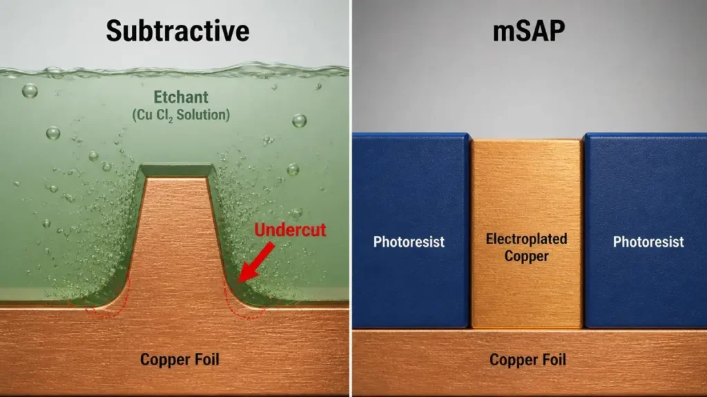
Microscopic Cross-Section Comparison of Subtractive Etching Undercut vs. mSAP Rectangular Trace Geometry
In standard subtractive fabrication, a panel laminated with full copper foil (typically 17–35 µm for outer layers, 9–17 µm for inner layers) undergoes dry-film photoresist lamination, LDI or contact exposure, develop, etch, and strip. The copper remaining after etching forms the circuit. The core problem: the etchant attacks the sidewalls of the trace while consuming the unwanted copper, causing undercut that widens the trace base relative to the top — directly degrading impedance repeatability and density.
In mSAP, the base laminate arrives with an ultra-thin electroless copper seed layer (1–3 µm). A photoresist is applied with the inverse pattern of the desired traces. Copper is electroplated into the exposed resist channels to the required height (typically 10–18 µm finished copper). After resist strip, the thin seed is removed by a controlled flash etch that consumes only the seed — less than 1 µm of lateral copper is removed from the plated traces, resulting in near-vertical sidewalls and trace widths held to ±2 µm of nominal.
2. Quantified Process Capability Comparison Table
| Parameter | Subtractive (Standard) | Subtractive (HDI) | mSAP | Full SAP |
| Min. Line/Space | 75/75 µm | 40/40 µm | 15–30 µm ✓ | 5–15 µm |
| Starting Cu Thickness | 17–35 µm | 9–17 µm | 1–3 µm (seed) | < 1 µm (EL Cu) |
| Trace Edge Definition | Moderate | Moderate | Sharp (±2 µm) | Very Sharp |
| Impedance Tolerance | ±10–12% | ±8–10% | ±5% or better | ±3–5% |
| Cu Material Utilization | ~30% | ~40% | ~85% | ~90% |
| Any-Layer HDI Support | Limited | Partial | Full ✓ | Full ✓ |
| Primary Applications | Standard boards | Mobile, consumer | SLP, SiP, AI PCB | IC substrates |
| Relative Production CAPEX | Low | Medium | Medium–High | Very High |
Data based on Hongda internal process qualification and published industry benchmarks (IPC-2226 Class C, 2025–2026). mSAP impedance results reflect TDR measurements per IPC-TM-650 2.5.5.7.
3. Copper Plating Uniformity and Edge Control in mSAP
Hongda’s mSAP line employs Vertical Continuous Plating (VCP) with real-time current density control (target ±3% across panel). Pulse-reverse plating waveforms suppress surface roughness on trace tops — a critical factor for high-frequency signal integrity, since surface roughness directly increases conductor loss at frequencies above 10 GHz (the Hammerstad-Jensen model predicts roughness-induced loss increase of 15–30% for a 1 µm Rz surface at 28 GHz compared to a smooth copper surface).
Additive suppressors and leveling agents in the plating bath further control edge sharpness. Our measured trace width distribution across a 507 × 407 mm production panel shows a process capability index (Cpk) of ≥1.33 for a 30 µm nominal trace width at ±3 µm tolerance, confirming production-ready mSAP on full panel format.
Material Compatibility: Low-Loss Laminates and mSAP Seed Adhesion
One of the technical barriers early in mSAP adoption was achieving reliable adhesion of the electroless copper seed to low-Dk, low-Df laminates (PTFE-composite, liquid crystal polymer, or hydrocarbon-ceramic materials) that have inherently low surface energy. Hongda has qualified mSAP on the following dielectric families:
- Modified epoxy/glass (Dk 3.5–4.2 / Df 0.008–0.012 at 10 GHz): Standard mSAP stack, highest volume.
- Megtron 6/7-class low-loss (Dk 3.3–3.6 / Df 0.002–0.004): Qualified for 56G PAM4 and 112G interfaces; plasma activation pre-treatment achieves ≥0.5 N/mm peel strength on seed copper.
- Ajinomoto GX-T series (Dk 3.1–3.3 / Df 0.003): Substrate-like applications; build-up film process with mSAP imaging at each layer increment.
Any Layer HDI PCB Capabilities: Architecture, Process Flow, and Engineering Challenges
1. Defining Any-Layer HDI and Its Engineering Demands
Standard HDI PCBs use laser-drilled blind microvias to connect adjacent layers, but these are typically confined to the outer 1+N+1 or 2+N+2 build-up layers. Any-Layer HDI — also called ELIC (Every-Layer Interconnection) — extends filled copper microvias to every dielectric layer of the stackup, enabling arbitrary interconnection between any two layers without routing through the board core.
This architecture is essential for modern high-density BGA fan-out where ball pitches of 0.35–0.5 mm leave insufficient space for traditional via-in-pad escape routing. Any-Layer HDI eliminates the constraint by allowing via stacking through all layers, placing connections exactly where the design requires them.
Engineering challenges unique to Any-Layer HDI include:
- Layer-to-layer registration accuracy: Each sequential lamination cycle introduces dimensional variation. Hongda uses X-ray panel registration before each LDI exposure step, achieving ±15 µm layer-to-layer registration tolerance — a prerequisite for stable stacked microvia columns.
- Stacked microvia reliability: Copper-filled stacked vias must survive thermal cycling without interface delamination. Hongda’s filled-via process (ECD copper fill with < 5 µm dishing per IPC-6012E Class 3 criteria) achieves > 500 cycles at −55°C to +125°C without electrical open failure.
- Dielectric thickness uniformity: Each laser-drillable dielectric layer must be uniform to ±8% or better to maintain via depth consistency, which directly affects laser energy parameters and via bottom quality.
- CTE mismatch management: In builds with 10 or more sequential laminations, cumulative Z-axis CTE stress can cause inner-layer pad cratering. Hongda’s laminate selection process mandates a Z-axis CTE < 50 ppm/°C for all build-up dielectrics used in Any-Layer configurations.
2. Any-Layer HDI Production Flow at Hongda
The Hongda Any-Layer HDI process integrates mSAP imaging at each build-up step rather than applying subtractive etching to thick laminate foils. The production sequence for a representative 16-layer Any-Layer HDI panel is:
- Core fabrication: Standard inner-layer imaging (mSAP or subtractive depending on L/S requirements), laminated and pressed.
- Sequential build-up, Layer N+1: Dielectric film lamination → CO₂/UV laser drilling of microvias (hole diameter 60–100 µm) → plasma desmear → electroless Cu seed → mSAP imaging → VCP copper plating → flash etch → AOI.
- Repeat for each additional build-up layer. Any-Layer HDI panels at Hongda are currently qualified to 8 build-up layers per side (maximum 20-layer total), with a development roadmap to 10+10.
- Final surface finish options: ENIG (3–5 µin Au / 120–240 µin Ni), ENEPIG (for wire-bond pads), OSP, or electrolytic hard gold for edge fingers.
3. Impedance Architecture in Any-Layer HDI Stacks
Impedance control in Any-Layer HDI demands layer-by-layer dielectric thickness management rather than relying on a single controlled-impedance layer. Hongda’s approach:
- Each build-up dielectric layer is measured by cross-section coupon (±0.5 µm resolution SEM) at the start, middle, and end of each production run.
- Trace widths for controlled impedance layers are adjusted per-lot based on actual measured dielectric thickness, using Polar Si9000e field-solver calculations.
- Differential pairs on Any-Layer HDI targets ±5% impedance from nominal, verified by TDR coupon on each production panel.
Key Equipment, Process Parameters, and Production Line Capabilities
1. Critical Equipment at Hongda’s mSAP Line
- Laser Drill: CO₂ + UV combined system, minimum hole diameter 60 µm, positional accuracy ±10 µm (3σ); drilling rate 2,000 holes/second.
- LDI (Laser Direct Imaging): Resolution 8 µm pixel; line width capability to 20 µm; panel size 600 × 530 mm; 3-sigma registration ±5 µm to fiducial.
- VCP (Vertical Continuous Plating): Plating uniformity ±3% (panel); current density 1.0–2.5 ASD; pulse-reverse waveform capability; real-time bath chemistry monitoring (Atotech Uniplate process).
- Electroless Copper Line: Seed deposition 1.0–3.0 µm; bath stability ± 0.2 µm/hr; inline thickness monitor by X-ray fluorescence (XRF).
- AOI (Automated Optical Inspection): Resolution 2 µm; false call rate < 200 ppm; inline after every imaging and plating step.
- X-ray Inspection: Layer registration verification on 100% of panels; defect detection capability for internal voids, cracks, and misregistration > 20 µm.
2. Production Capacity and Yield Metrics
- Monthly production capacity: 15,000 m² of mSAP-capable HDI panels (scalable to 20,000 m² with current equipment).
- Target production first-pass yield: ≥ 95% for 8-layer HDI with 30/30 µm mSAP traces.
- Prototype-to-production lead time: 5–7 working days for 2–4 layer mSAP; 10–14 working days for 8–16 layer Any-Layer HDI.
- Panel size supported: Up to 507 × 610 mm; minimum 50 × 50 mm.
Testing, Verification, and Quality Control in mSAP HDI Manufacturing
1. In-Process Monitoring
Quality in mSAP HDI is built into the process at every step, not inspected in at the end. Hongda’s in-process control protocol includes:
- Copper thickness: XRF measurement every 2 hours on production panels; target plated copper height 15 ± 2 µm for standard mSAP; tolerance tightens to ± 1 µm for impedance-critical layers.
- Plating bath chemistry: Continuous circulation and inline concentration monitoring for all major constituents (Cu²⁺, H₂SO₄, chloride, suppressor, accelerator, leveler); automatic dosing system maintains ±5% of target.
- Laser drill quality: 100% AOI on drilled panels; cross-section coupon (1 per lot, 10 vias minimum) for SEM verification of hole wall quality, smear removal, and copper coverage.
- LDI alignment: 100% panel pre-registration by X-ray fiducial read; NG panels rejected before resist lamination — a zero-defect gate on registration.
2. Final Electrical and Mechanical Validation
- Impedance testing: 100% TDR on controlled-impedance lots per IPC-TM-650 2.5.5.7; results reported with each shipment.
- Continuity and isolation: 100% E-test (flying probe or fixture) per IPC-9252A; isolation resistance > 100 MΩ at 250 VDC.
- Thermal reliability: Thermal shock per IPC-TM-650 2.6.7.2 (−55°C / +125°C, 100 cycles); IST (Interconnect Stress Test) per IPC-TM-650 2.6.26 to 500 cycles equivalent for Any-Layer HDI qualification lots.
- Cross-section metallography: 3 coupons per lot for filled-via dishing (< 5 µm), plated copper grain structure, and dielectric integrity verification.
- Ion chromatography (IC): Ionic cleanliness testing per IPC-TM-650 2.3.28 — standard on all SiP and BGA-carrier products.
3. Common Defect Modes and Prevention
The most frequently encountered failure modes in mSAP HDI and Hongda’s process responses:
- Seed layer delamination: Prevented by controlled plasma desmear time (target 20–25 min at 250 W) and same-day electroless copper deposition after plasma treatment.
- Trace necking or opens: Caused by resist adhesion failure during plating. Prevented by automated resist pin-hole inspection (LDI comparison) and temperature-controlled lamination.
- Microvia copper void: Flash etch over-removal at via capture pads. Controlled by real-time etch rate monitoring and timed bath refresh.
- Registration drift in sequential builds: Addressed by per-layer X-ray registration before each LDI exposure; any panel exceeding ±20 µm drift is re-registered or scrapped.
Production Case Studies and Engineering Validation Data
1. Case Study: SLP for Mobile AI Processor BGA Escape
Customer requirement: 0.4 mm pitch µBGA escape routing for a 12 × 12 mm AI SoC; 8 signal layers + 2 power/ground planes; overall board thickness 0.65 mm; operating frequency to 56 Gbps PAM4.
- Trace/space achieved: 30/30 µm mSAP on 4 inner build-up layers; 40/40 µm subtractive on core.
- Impedance result: 100Ω ± 4.8% (TDR, 25 pairs measured per coupon across 3 production lots).
- Thermal cycling: 0 failures after 300 cycles (−40°C to +125°C), equivalent to 7 years in-field reliability at standard JEDEC conditions.
- Production yield: 96.3% first-pass for 1,500 panels produced in validation run.
2. Case Study: Any-Layer HDI for SiP Wearable Module
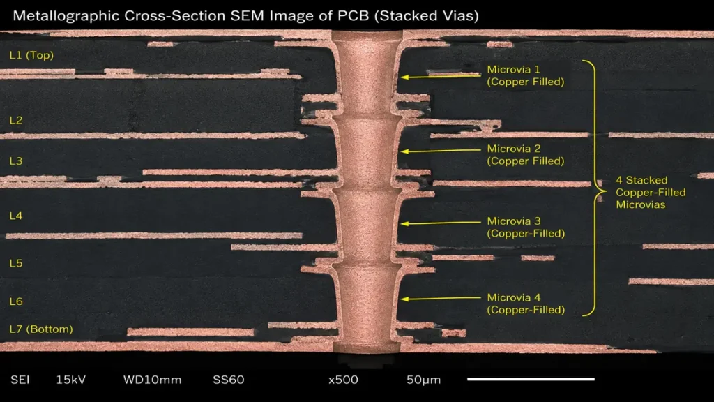
SEM Metallographic Cross-Section of 4 Stacked Copper-Filled Microvias showing perfect alignment and zero voids from L1 to L7
Customer requirement: 12-layer Any-Layer HDI, 4+4+4 build-up, carrying RF, digital, and power on a 28 × 28 mm footprint; stacked microvias through all layers.
- Microvia column: 4 stacked filled microvias (80 µm diameter), cross-section dishing < 3 µm per via.
- Min. trace: 30/30 µm mSAP on all build-up layers.
- Layer registration: ±12 µm average, worst-case ±18 µm, all within ±20 µm spec.
- IST reliability: 480 cycles passed (IPC-TM-650 2.6.26); production qualification achieved.
- Substrate material: Panasonic Megtron 7 build-up film; Dk 3.4 / Df 0.002 at 10 GHz.
DFM Guidelines for mSAP HDI and Any-Layer HDI PCB Design
1. Critical Design Rules for mSAP Trace and Via Geometry
Engineers specifying boards for mSAP fabrication at Hongda should apply the following design rules from the initial layout stage. DFM reviews are available at no charge before order placement.
| Design Parameter | Recommended Value (mSAP) | Notes |
| Min. Line/Space | 30/30 µm production; 20/20 µm on request | Verify with pre-DFM check |
| Min. Annular Ring | 50 µm (laser via), 75 µm (mechanical) | X-ray inspection on every panel |
| Microvia Diameter | 60–100 µm (stacked), 75–150 µm (staggered) | Confirm aspect ratio ≤ 0.8:1 for copper fill |
| Diff. Pair Spacing | ≥ 3× trace width from adjacent signals | Critical for 56G PAM4 / 112G applications |
| Impedance Target | 50Ω single-ended; 100Ω differential | Tolerance ±5% guaranteed |
| Preferred Substrate Dk/Df | Dk 3.0–3.5 / Df < 0.003 at 10 GHz | Low-loss laminates for RF & AI accelerator |
2. Stack-Up and Material Recommendations
- For designs operating above 10 GHz, specify Dk ≤ 3.5 and Df ≤ 0.004 laminates. Pair low-loss core material with compatible build-up film (same manufacturer family where possible to minimize CTE mismatch).
- Minimum dielectric thickness between mSAP signal layer and adjacent reference plane: 50 µm for 50Ω single-ended; 65 µm for 100Ω differential with 30 µm trace width. Thinner dielectrics require narrower traces and tighter LDI control.
- For any-layer HDI stacks exceeding 8 total layers, specify Z-axis CTE < 50 ppm/°C for all dielectric materials to prevent pad cratering in thermal cycling.
- Thermal vias: Minimum 0.2 mm drill (mechanical), copper-filled, on 0.4 mm pitch grid for effective heat spreading in power stages.
3. Design Delivery Requirements
To initiate a Hongda mSAP/HDI project, please provide:
- Gerber RS-274X or ODB++ fabrication data with all copper, soldermask, silkscreen, and drill layers.
- IPC-2581 or equivalent netlist for E-test reference.
- IPC-2226 or equivalent stack-up specification with impedance targets, dielectric material preferences, and copper thickness per layer.
- BOM with component footprints for DFM review of pad geometry, via-in-pad requirements, and assembly process compatibility.
Production Capabilities, Commercial Conditions, and Quality Assurance Commitments
1. What Hongda Guarantees in Writing
- mSAP trace/space: 30/30 µm production standard; 20/20 µm available with engineering review (no additional tooling charge for qualifications).
- Any-Layer HDI: Up to 20 total layers (10+core+10 build-up sequence) in production; larger configurations on request.
- Impedance tolerance: ±5% from nominal for all controlled-impedance mSAP products (TDR-verified, certificate supplied).
- Layer registration: ±20 µm maximum for any-layer HDI; ±15 µm target.
- First-article sample delivery: 5–7 working days (standard mSAP HDI, ≤ 8 layers); 10–14 working days (Any-Layer HDI ≤ 20 layers).
2. Certifications and IP Protection
- Quality management system: ISO 9001:2015 certified; IATF 16949 (automotive) in process.
- Reliability standards: Products conform to IPC Class 2 as standard; IPC Class 3 available with explicit specification.
- Environmental compliance: RoHS 3 (EU 2015/863) and REACH SVHC < 0.1% by weight; halogen-free build-up materials available.
- IP protection: NDAs signed before any customer design data transfer; dedicated servers for customer file storage; no design data shared across customer accounts.
- Minimum order quantity: 1 piece (prototype); volume pricing from 50 panels.
mSAP and Any-Layer HDI as the Production Standard for Next-Generation PCBs
The evidence presented in this document establishes that mSAP is not an emerging technology — it is the production-proven process for achieving sub-40 µm trace resolution, tight impedance control, and reliable any-layer interconnect architectures that the current generation of AI, RF, and SiP electronics demand.
Shenzhen Hongda Circuit Technology Co., Ltd. operates mSAP at full production scale, with verified process capability, published yield data, and completed reliability qualification for Any-Layer HDI. Our engineering team is equipped to support design entry through production ramp, with DFM reviews, impedance modeling, and test report generation included in standard service.
© 2026 Shenzhen Hongda Circuit Technology Co., Ltd. All rights reserved. Technical data subject to change without notice. Contact engineering team for latest specifications.
FAQ
What is the difference between mSAP and subtractive etching in HDI fabrication?
The fundamental difference lies in how the copper traces are formed. Conventional subtractive etching starts with a full copper foil (9–35 µm) and chemically etches away unwanted areas
. As line width drops below 40 µm, chemical etchants attack the trace sidewalls laterally, causing severe undercut and trapezoidal cross-sections that degrade impedance consistency
In contrast, the Modified Semi-Additive Process (mSAP) utilizes an ultra-thin 1–3 µm electroless copper seed layer
. Traces are electroplated vertically into precise dry-film resist channels, followed by a controlled flash etch to remove the seed layer
. This achieves near-vertical sidewalls (sharp trace edge definition within ±2 µm) and tight impedance control (±5% or better), which are essential for chip-level and advanced packaging applications
What are your factory’s production capabilities for Any-Layer HDI PCBs?
Shenzhen Hongda Circuit Technology operates a dedicated, high-precision mSAP production line capable of fabricating Any-Layer HDI PCBs (Every-Layer Interconnection / ELIC) up to 20 total layers (10+core+10 sequential build-up)
Our advanced manufacturing setup features
1. Trace Resolution: Standard production at 30/30 µm (1.2/1.2 mil) line/space, with a technical roadmap scaling down to 20/20 µm
2. Microvia Execution: CO₂ + UV combined laser drilling down to 60 µm hole diameters with a 3-sigma positional accuracy of ±10 µm
3. Layer-to-Layer Registration: Active X-ray panel registration combined with Laser Direct Imaging (LDI) achieving a strict ±15 µm to ±20 µm alignment tolerance across high-layer sequential laminations
Can your mSAP process handle low-loss laminates for AI accelerators and IC substrates?
Yes. One of the primary engineering challenges in mSAP adoption is ensuring strong copper seed adhesion to low-surface-energy, high-frequency dielectrics. Hongda has fully qualified and verified its mSAP line across premium low-loss material families:
1. Megtron 6 / Megtron 7-class: Ideal for 56G and 112G PAM4 ultra-high-speed AI server architectures. We utilize specialized plasma activation pre-treatment to guarantee a seed copper peel strength of ≥0.5 N/mm.
2. Ajinomoto GX-T Series: Optimized for substrate-like PCBs (SLP) and System-in-Package (SiP) modules using automated sequential build-up film imaging
3.Modified Epoxy/Glass: For high-volume, cost-optimized dense HDI configurations operating up to 10 GHz.
How does Hongda guarantee yield and reliability for 1.2/1.2 mil (30 µm) ultra-fine line traces?
We don’t just promise capability; we back it up with a quantified ≥95% first-pass yield for 8-layer mSAP boards with 30/30 µm traces
Our quality control infrastructure involves:
1. Plating Uniformity: We use Vertical Continuous Plating (VCP) with pulse-reverse waveforms, maintaining a strict ±3% plating uniformity to suppress trace surface roughness and control high-frequency conductor loss
2. Process Stability: Our line delivers a Process Capability Index (Cpk) of ≥1.33 for 30 µm nominal trace widths
3. Rigorous Validation: Every production lot undergoes 100% Time-Domain Reflectometry (TDR) impedance testing (guaranteeing ±5% tolerance), 100% Automated Optical Inspection (AOI) down to 2 µm resolution, and Interconnect Stress Testing (IST) up to 500 thermal cycles (−55°C to +125°C) to ensure zero stacked via delamination
What are the critical DFM design rules and submission requirements for an mSAP HDI project?
To ensure optimal manufacturability and high yields, layout engineers should implement the following baseline mSAP DFM guidelines:
1. Traces & Vias: Maintain a 30/30 µm line/space standard. Laser microvia annular rings should be ≥50 µm, with a via aspect ratio held ≤ 0.8:1 for perfect copper filling.
2. Signal Integrity: Differential pairs should maintain a spacing of ≥ 3× the trace width from adjacent signals to mitigate cross-talk in 56G/112G PAM4 setups.
3. Materials: For stacks exceeding 8 layers, specify a dielectric with a Z-axis CTE < 50 ppm/°C to prevent pad cratering during sequential laminations
Find Out About Us: Delivering Top-Tier Fabrication for Both AI & Conventional PCBs
Navigating the line between cutting-edge innovation and high-volume, cost-effective production shouldn’t be a compromise. At Shenzhen Hongda Circuit Technology (PCBKR), we bridge this gap by elevating the manufacturing standards for both high-performance AI hardware and traditional multi-layer PCBs.
By integrating advanced manufacturing methodologies across all production lines, we bring an elite level of precision to traditional PCB fabrication. Our standard boards benefit from enhanced interlayer alignment tolerances (down from ±75μm to within ±25μm) and tightened differential impedance control (±5%). Supported by 100% 3D X-Ray (AXI) inspection, your conventional boards achieve chip-level reliability, superb signal stability, and near-100% yield.
Your Strategic Manufacturing Partner
We proudly stand as a dual-capability partner: offering the elite technical ceiling required for next-gen AI hardware, while maintaining the exceptional flexibility, rapid turnaround, and unmatched cost-efficiency needed for mid-to-high-volume traditional board campaigns. You get zero-defect reliability without the premium overhead or bureaucracy of massive tier-1 factories.
Ready to upgrade your hardware’s reliability?
Submit your Gerber files today for an agile engineering review and a highly competitive quote.
Contact our experts: sales@pcbkr.com
About Author
David Chen https://www.linkedin.com/in/pcbcoming
David Chen boasts an extensive professional background in PCBA manufacturing, PCBA testing, and PCBA optimization, with specialized expertise in high-precision PCBA fault analysis and rigorous PCBA reliability testing. The author has worked with high-layer-count server PCB fabrication, ultra-low-loss backplane stackups, and thermo-mechanical reliability optimization for AI infrastructure projects involving 112G and 224G PAM4 architectures. Skilled in complex circuit design and cutting-edge advanced PCB manufacturing processes, he delivers solutions that elevate product durability and performance across industrial applications. His technical articles focusing on PCBA manufacturing workflows and testing methodologies are widely cited by industry peers, research institutions, and technical platforms, solidifying his reputation as a recognized technical authority in the global circuit board manufacturing sector.