How to Meet Tight NPI Deadlines with Quick Turn HDI PCB Prototype Services in 2026
Introduction:Why HDI PCB Fast Turnaround Is More Critical Than Ever in 2026
The pressure on hardware engineering teams has never been higher. In 2026, product release cycles in consumer electronics, AI infrastructure, automotive ADAS, and medical devices have compressed to the point where a two-week PCB fabrication delay can cost a company millions in delayed revenue, missed design windows, or lost investor confidence.
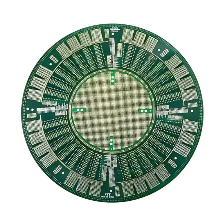
High-Density Interconnect (HDI) PCBs sit at the center of nearly every advanced electronic device — from 5G mmWave modules and edge AI accelerators to wearable biosensors and satellite communication payloads. These boards are not simple: they demand microvias, laser-drilled blind and buried vias, any-layer interconnects, and sub-2-mil trace geometries. Historically, that technical complexity came with a painful trade-off: long lead times. Finding a reliable partner who offers true fast turnaround hdi fabrication china wide has been a persistent challenge for engineering teams
The question hardware program managers and senior engineers are asking in 2026 is no longer ‘Can we get an HDI board fast?’ — it’s ‘Can we get a production-grade HDI board fast, without sacrificing yield, signal integrity, or traceability?’
This article addresses exactly that, combining the latest 2026 manufacturing advances with a procurement framework for engineering teams managing NPI (New Product Introduction) schedules under real-world constraints.
Speed Defined by Numbers: What Does ‘Fast Turnaround HDI Fabrication’ Mean in 2026?
The word ‘fast’ is meaningless without a number behind it. When you are searching for a qualified quick turn hdi pcb prototype supplier, here is what a credible manufacturer in China should be able to commit to in 2026:
| Stack-Up Type | Layer Count | Fastest Turnaround | Standard Turnaround |
| 1+N+1 HDI | 4–8 Layers | 3–4 Business Days | 7–10 Business Days |
| 2+N+2 HDI | 6–12 Layers | 4–5 Business Days | 10–12 Business Days |
| Any-Layer HDI (ELIC) | 8–20 Layers | 5–7 Business Days | 14–18 Business Days |
| Any-Layer + mSAP | 12–24 Layers | 6–8 Business Days | 18–22 Business Days |
| Rigid-Flex HDI | 4–16 Layers | 7–10 Business Days | 18–25 Business Days |
These timelines assume design files (Gerber/ODB++/IPC-2581) arrive complete and DFM-clean. Where they do not — and they rarely do — the differentiating factor becomes how quickly the manufacturer’s CAM engineering team can identify issues, resolve them, and restart the clock.
2026 Industry Context: According to supply chain intelligence tracked through early 2026, lead times for complex Any-Layer HDI boards at Tier-1 volume fabs average 18–24 days. A quick-turn specialist with 24/7 CAM operations and dedicated fast-track lines can compress this to 5–7 days without changing the process chemistry or material stack — a capability that simply did not exist at scale before 2024.
2026 HDI PCB Manufacturing Technology: What Has Genuinely Changed?
Many suppliers claim to offer ‘2026-ready’ technology. The following are the advances that are now commercially available from leading quick-turn HDI fabricators and that directly affect NPI feasibility:
Modified Semi-Additive Process (mSAP) for Sub-2-Mil Trace Geometries
Traditional subtractive etching struggles below 3/3 mil (line/space). In 2026, mSAP — the same copper deposition process used in advanced IC substrates — is now offered by select fast-turn PCB manufacturers for high-speed signal routing down to 1.5/1.5 mil. This unlocks escape routing from 0.3 mm BGA components without violating IPC-6012F Class 3 specifications.
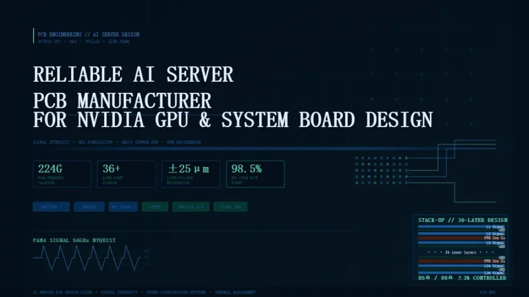
For AI accelerator boards, networking ASICs, and 5G radio units handling 112G PAM4 and emerging 224G signaling, mSAP capability is no longer optional — it is the difference between a board that works and one that cannot route cleanly.
Laser Via Technology: UV DPSS and CO2 Hybrid Drilling
The latest laser drilling platforms deployed in 2025–2026 combine ultraviolet DPSS (Diode-Pumped Solid-State) lasers for copper-capped microvias with CO2 laser systems for dielectric ablation. The result is via diameters as small as 50 microns with tighter positional accuracy (±15 µm vs. the older ±25 µm standard). For stacked microvia structures and copper-filled VIPPO (Via-In-Pad Plated Over) configurations required by high-pin-count BGA devices, this translates directly into higher first-pass yield — reducing the risk of expensive respins during NPI.
AI-Assisted DFM and Automated CAM Review
One of the most significant 2026 developments is the deployment of machine-learning-assisted DFM (Design for Manufacturability) tools directly within fabricator CAM workflows. Leading suppliers have integrated AI engines that can scan Gerber or ODB++ files and flag issues — minimum annular ring violations, acid trap geometries, impedance discontinuities, and solder mask web failures — within minutes of file upload.
This is not a gimmick. In practice, it compresses what used to be a 12–24 hour manual CAM review into a 90-minute automated pre-screen, with a human engineer validating edge cases. For NPI programs where every hour matters, this single capability improvement can save an entire business day off the schedule.
Oxide-Alternative Surface Bonding for Thin Dielectric Stacks
HDI boards frequently use prepreg materials as thin as 50–75 µm between layers. Traditional brown oxide or black oxide adhesion treatments were prone to variability at these thicknesses. In 2026, leading fabricators have standardized on horizontal conveyorized oxide-alternative (OA) processes with tighter bath chemistry control, delivering more consistent peel strength and reducing delamination risk — a failure mode that historically inflated NPI rework rates.
Digital Twin Process Monitoring and Traceability
For customers in aerospace, medical, and automotive sectors, full process traceability from raw laminate to final test is now expected at the quick-turn level. The best 2026-capable fabs operate digital twin environments where each panel’s process parameters — etch chemistry concentrations, laser energy, plating current density, lamination press profiles — are logged per job, exportable as a PDF or structured data file alongside the shipped boards. This is not standard across the industry, but it is a qualifying criterion for serious procurement decisions.
Overcoming the Engineering Query (EQ) Delay: The 24/7 DFM Fast-Track Advantage
The single most common cause of NPI schedule slippage is not manufacturing complexity — it is the engineering query (EQ) loop. A customer submits Gerber files late Friday (California time). The China-based fab’s engineers are already gone for the evening. By the time a DFM issue surfaces and an EQ is generated, 18–24 hours have passed before the customer even sees the question.
A 2026-capable quick-turn HDI supplier should eliminate this entirely through:
- A 24/7 CAM engineering team operating in three-shift rotations, ensuring that no file submission sits unreviewed for more than two hours regardless of the time zone differential.
- A structured EQ Matrix format sent to the customer, not a wall of text — listing each issue, its location in the design (layer, coordinates, net name), the proposed fix, and a yes/no confirmation field. This format reduces reply time from customers by an average of 60%.
- A ‘silent DFM’ option for experienced customers: the fab applies standard design rule corrections within pre-agreed parameters without raising an EQ, streamlining the process further for repeat customers with known design styles.
Real-World Benchmark: An engineering team submitting Any-Layer HDI Gerbers on a Monday at 5:00 PM PST should receive a complete DFM report and commercial quote before 9:00 AM Tuesday PST — even accounting for the overnight gap. This is the operational standard that separates professional quick-turn HDI fabricators from low-cost sample shops.
From HDI PCB Prototype to Mass Production: Eliminating the ‘Transfer Risk’ Problem
A frustration that every experienced hardware PM knows: the prototype passed qualification at the quick-turn fab, but when the same design transferred to the volume production factory, yields dropped and re-spins were required. This ‘transfer risk’ is not inevitable — it is an artifact of using two different manufacturers with different equipment baselines, material qualifications, and process windows.
The right quick-turn HDI PCB supplier in 2026 eliminates this risk through a unified one-stop solution:
Same Materials from Prototype to Production
High-volume-grade laminates such as Shengyi S1000-2, Panasonic Megtron 6/7, Rogers 4350B, and Isola I-Tera MT40 should be available for quick-turn prototype quantities — not just for production runs. When the engineer qualifies a design on Megtron 6 at the prototype stage, they should be able to confirm that the mass production run will use Megtron 6 from the same qualified supply chain, with the same dielectric constant and Dk/Df values that the signal integrity model assumed.
Single CAM Data Set Across Both Phases
The CAM files, impedance calculations, and panelization layouts generated during prototyping should carry forward without modification to the production phase. Any deviation — even a minor panelization change — introduces a new variable that may affect yield. Leading suppliers maintain a locked CAM data package that travels with the job number from first article through mass production sign-off.
Controlled Impedance Consistency
HDI boards for high-speed digital applications typically require controlled impedance traces with tolerances of ±8% or tighter. In 2026, impedance is verified not just by coupon measurement at end-of-line, but through inline dielectric thickness monitoring and automated copper plating thickness feedback loops during the build. This means prototype impedance measurements are predictive of production performance — not just incidental.
Technical Capability Checklist: Evaluating Your Fast Turnaround HDI Fabrication China Partner
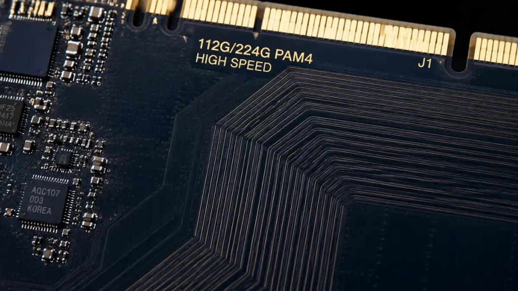
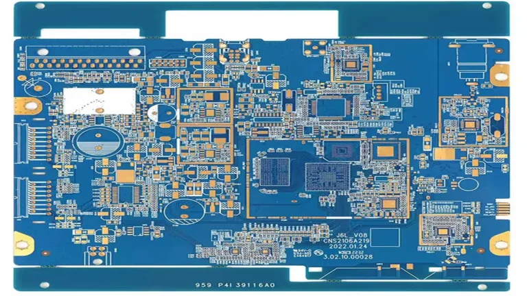
Inspection detail of a 112G/224G PAM4 high-speed routing fabric with tight geometric tolerance and gold finger finish.
When evaluating a quick-turn HDI PCB manufacturer for demanding applications, request documentation confirming the following 2026-standard capabilities:
| Capability Category | Specification (2026 Best-in-Class) | Why It Matters |
| Stack-Up Range | 1+N+1 through Any-Layer (ELIC), up to 24 layers | Covers low-complexity to advanced AI/5G designs |
| Minimum Line / Space | 1.5 / 1.5 mil (mSAP process) | Required for 0.3 mm BGA escape routing |
| Microvia Diameter | 50 µm (laser drilled) | Enables high-density via arrays |
| Microvia Positional Accuracy | ±15 µm | Critical for stacked via reliability |
| Copper Fill (VIPPO) | Fully planar-filled microvias | Required for thermal via and BGA applications |
| Controlled Impedance Tolerance | ±5% (with inline monitoring) | Ensures signal integrity for 112G+ SerDes |
| Surface Finish Options | ENIG, ENEPIG, Immersion Silver, OSP, Hard Gold | Covers RF, wire-bond, and solderability needs |
| Max Copper Weight | 4 oz outer / 2 oz inner | Power delivery for high-current applications |
| Thermal Management | Embedded heat slug, cavity routing | Required for high-power RF and power modules |
| IPC Certification | IPC-6012F Class 2 / Class 3 certified | Traceability and qualification documentation |
| Signal Speed Support | 112G PAM4 validated; 224G design support | Next-generation networking and AI fabric boards |
How to Evaluate and Qualify a Quick-Turn HDI PCB Supplier: A Procurement Framework
Sourcing a new HDI PCB supplier under NPI pressure is high-stakes. The following framework helps procurement engineers move efficiently from shortlist to qualified supplier:
Step 1 — Verify Equipment, Not Just Claims
Request the equipment list for laser drilling, LDI (Laser Direct Imaging), and AOI (Automated Optical Inspection) systems. Legitimate quick-turn HDI fabs in 2026 operate LDI systems from suppliers such as Orbotech or Ucamco — not older phototool-based exposure. Laser drilling systems should be from established platforms capable of 50 µm microvias. If a supplier cannot name their equipment, that is a red flag.
Step 2 — Request a Capability Sample and Cross-Section Report
Before committing to a first NPI run, request a capability verification coupon — a standard test vehicle with representative HDI features at your target specifications. Alongside the boards, request a cross-section report showing microvia geometry, copper fill quality, and layer-to-layer registration. A professional HDI fab will provide this as a standard service; a sample shop often cannot.
Step 3 — Assess Communication and EQ Response Time
Send a test Gerber package — ideally with a few known, minor DFM issues embedded — and measure response time and quality. A supplier targeting serious NPI customers will respond within two hours with a structured EQ matrix. If the response takes 24 hours and arrives as a casual email, that supplier’s actual fast-turn claim should be treated with skepticism.
Step 4 — Confirm Material Traceability and Certification
Ask for a sample material certification (C of C) from a recent job. It should identify the specific laminate by manufacturer part number, lot number, and Dk/Df values. IPC-6012F Class 3 certification should be confirmed by a third-party audit report, not just a logo on a marketing page.
Stop Letting Fabrication Define Your NPI Calendar
In 2026, a hardware team’s competitive advantage is defined by how quickly they can go from silicon-validated design to working prototype in the hands of the integration team. Fabrication should be a controlled, predictable variable — not the wildcard that blows up the schedule.
A qualified quick-turn HDI PCB fabrication partner in China should deliver:
- 3–7 business day turnaround on complex HDI stack-ups, using production-grade materials and equipment.
- 2-hour DFM review and EQ response, regardless of the customer’s time zone.
- Full process traceability and impedance documentation from first article to production.
- A seamless, single-CAM-data transition from NPI prototype to volume manufacturing — zero transfer risk.
- mSAP capability, VIPPO copper fill, and 112G/224G PAM4 signal integrity support for next-generation designs.
Ready to Accelerate Your NPI Program with an Experienced HDI PCB Supplier? Submit your Gerber or ODB++ files to our quick turn hdi pcb prototype fast-track team today.
Submit your Gerber or ODB++ files and receive a comprehensive DFM review plus commercial quote within 2 hours. Our CAM engineering team operates 24/7 to ensure your fast-track request is never delayed by time zones. Email: sales@pcbkr.com | Fast Track Desk | www.pcbkr.com
FAQ
What is the realistic lead time for quick-turn HDI PCB prototypes from a China supplier in 2026?
For 1+N+1 and 2+N+2 HDI designs in the 4–12 layer range, a legitimate quick-turn specialist can deliver in 3–5 business days from DFM approval. Any-Layer HDI (ELIC) boards typically require 5–7 business days. These timelines apply when the design files are complete and DFM-clean. Add 1–2 days if engineering queries require customer input. Shipping via DHL Express from China to North America or Europe adds approximately 2–3 days, making total elapsed time from order to receipt approximately 7–10 calendar days for most NPI scenarios. Beware of suppliers quoting ‘3-day’ turnaround on Any-Layer HDI — confirm whether that includes DFM review time or starts only after file approval.
Can a quick-turn HDI PCB manufacturer in China support Class 3 IPC-6012 quality requirements?
Yes — but only from a subset of fabs. IPC-6012F Class 3 compliance requires documented process control, specific minimum annular ring and copper thickness specifications, and lot traceability. Not every China-based quick-turn PCB shop maintains IPC-6012 Class 3 certification. When evaluating suppliers, request a copy of their IPC certification documentation and ask whether the fast-turn process line uses the same process parameters as the standard production line. At some facilities, ‘fast turn’ means a different line with different controls — which may not meet Class 3 requirements. A qualifying supplier should be able to ship Class 3-compliant boards on both fast-turn and standard schedules, with no process compromises.
How do I ensure that HDI PCB prototypes and mass production boards have matching impedance and electrical performance?
This is one of the most technically important questions in HDI procurement, and it is frequently overlooked until a transfer-to-production problem surfaces. To ensure matching performance across NPI and production phases: (1) Specify the exact laminate by manufacturer and part number — do not accept substitutions. (2) Require controlled impedance coupons on every prototype panel, with test data reported in the delivery package. (3) Confirm that the fab uses LDI (Laser Direct Imaging) rather than phototool exposure — LDI delivers ±5 µm feature accuracy vs. ±25 µm for phototools, which directly affects trace width consistency and impedance. (4) Request that the CAM data package is locked and carried forward to the production run without modification. Any change to layer stack-up, trace width adjustments, or panelization should require a formal ECO with a re-verification coupon.
What HDI PCB manufacturing technologies are required for 112G PAM4 and next-generation AI chip designs in 2026?
Boards supporting 112G PAM4 SerDes interfaces — used in switches, AI accelerator interconnects, and coherent optical modules — require a specific set of fabrication capabilities that not all HDI fabs can provide. At minimum, the fab must offer: (1) Low-loss laminates with Dk below 3.5 and Df below 0.004 at 10 GHz (e.g., Panasonic Megtron 7, Isola I-Tera MT40). (2) mSAP or semi-additive copper patterning for trace widths below 2 mil with consistent edge definition. (3) Copper-filled microvias (VIPPO) to minimize stub effects on vertical transitions through the stack-up. (4) Controlled impedance to ±5% with inline dielectric measurement. (5) Via-in-pad technology with planar finish for 0.4 mm and 0.3 mm BGA component landing pads. For 224G designs entering the lab phase in 2025–2026, add requirements for glass-fiber weave management (spread glass or resin-coated foil) to minimize fiber weave effect on differential pairs.
How do I compare HDI PCB quotes from multiple China suppliers without comparing apples to oranges?
This is the practical reality of procurement: two quotes for the same Gerber files from two different suppliers can vary by 40–60% and still represent entirely different products. To create a fair comparison, require each supplier to quote against a standardized specification sheet that includes: (1) Laminate material by manufacturer and part number. (2) Surface finish type and specification (e.g., ENIG per IPC-4552 Rev B). (3) Solder mask by name and color. (4) Impedance tolerance and verification method. (5) IPC Class (2 or 3). (6) Panel size and quantity per panel. (7) Electrical test method (flying probe vs. fixture). (8) Delivery terms (EXW factory vs. DDP destination). A supplier that cannot or will not fill in all fields on a structured quote template is, by definition, not controlling those variables — which means the delivered product quality is uncontrolled. Price alone is never a valid comparison metric for HDI PCB sourcing.
Navigating the line between cutting-edge innovation and high-volume, cost-effective production shouldn’t be a compromise. At Shenzhen Hongda Circuit Technology (PCBKR), we bridge this gap by elevating the manufacturing standards for both high-performance AI hardware and traditional multi-layer PCBs.
By integrating advanced manufacturing methodologies across all production lines, we bring an elite level of precision to traditional PCB fabrication. Our standard boards benefit from enhanced interlayer alignment tolerances (down from ±75μm to within ±25μm) and tightened differential impedance control (±5%). Supported by 100% 3D X-Ray (AXI) inspection, your conventional boards achieve chip-level reliability, superb signal stability, and near-100% yield.
Your Strategic Manufacturing Partner
We proudly stand as a dual-capability partner: offering the elite technical ceiling required for next-gen AI hardware, while maintaining the exceptional flexibility, rapid turnaround, and unmatched cost-efficiency needed for mid-to-high-volume traditional board campaigns. You get zero-defect reliability without the premium overhead or bureaucracy of massive tier-1 factories.
Ready to upgrade your hardware’s reliability?
Submit your Gerber files today for an agile engineering review and a highly competitive quote.
Contact our experts: sales@pcbkr.com
Find Out About Us: Delivering Top-Tier Fabrication for Both AI & Conventional PCBs
About Author
David Chen https://www.linkedin.com/in/pcbcoming
David Chen boasts an extensive professional background in PCBA manufacturing, PCBA testing, and PCBA optimization, with specialized expertise in high-precision PCBA fault analysis and rigorous PCBA reliability testing. The author has worked with high-layer-count server PCB fabrication, ultra-low-loss backplane stackups, and thermo-mechanical reliability optimization for AI infrastructure projects involving 112G and 224G PAM4 architectures. Skilled in complex circuit design and cutting-edge advanced PCB manufacturing processes, he delivers solutions that elevate product durability and performance across industrial applications. His technical articles focusing on PCBA manufacturing workflows and testing methodologies are widely cited by industry peers, research institutions, and technical platforms, solidifying his reputation as a recognized technical authority in the global circuit board manufacturing sector.