DFM Design Rules, Via Optimization, and Differential Pair Routing for AI-Era Electronics
The printed circuit board is no longer just a passive carrier of components. In 2026, as AI servers, 400G data center switches, and autonomous driving compute platforms push signal speeds beyond what traditional layout practices can reliably support, the PCB has become a precision high-frequency transmission medium. The gap between what design engineers simulate in software and what a fabrication facility can consistently manufacture is wider than most procurement teams realize — and that gap is where most project delays and respins are born.
Shenzhen Hongda Circuit Technology Co., Ltd. has manufactured high-density, impedance-controlled PCBs for global customers across defense, telecom, medical, and industrial markets. This article draws on our factory-floor experience to translate the latest 2026 PCB manufacturing technology into design rules that engineers can act on immediately, and purchasing professionals can use to evaluate supplier capability with confidence.
What Is a High-Speed Signal in PCB Design — and Why It Changes Everything in 2026
Engineers sometimes define “high-speed” by clock frequency alone. That is a shortcut that leads to underspecified boards. The more precise definition is based on signal rise time: when the edge rate of a digital signal is fast enough that the electrical length of a trace becomes a significant fraction of the signal’s wavelength, transmission line effects dominate and standard PCB layout rules break down.
In practical terms, this applies to PCIe Gen 5 and Gen 6 lanes, DDR5 and LPDDR5 memory buses, multi-gigabit SerDes interfaces, and 100G/400G Ethernet PHY connections — all of which have become standard in 2026 product designs. It also increasingly applies to USB4, Thunderbolt 5, and CXL 3.0 interconnects appearing in consumer and edge computing hardware.
When a signal behaves as a transmission line, four effects must be managed simultaneously: impedance discontinuities that cause reflections back toward the source; signal attenuation losses that degrade the eye opening at the receiver; crosstalk between adjacent traces that corrupts data on neighboring channels; and electromagnetic interference that can cause regulatory failure. None of these can be solved by the PCB designer working in isolation. All of them require close coordination with the fabrication facility.
The 2026 landscape adds a new dimension: AI accelerator boards using silicon interposers, co-packaged optics, and chiplet architectures demand multi-layer PCBs with 20+ copper layers, microvia arrays, and embedded passive components that only a small number of advanced PCB manufacturers can reliably produce.
High-Speed PCB DFM Challenges: The Manufacturing Perspective on Design for Manufacturability
Design for Manufacturability — DFM — is the discipline of building fabrication constraints into a design before the files are released to the factory. The inverse, releasing a design and discovering fabrication conflicts during engineering review, is the single largest cause of PCB project delays. In our experience processing DFM reviews for customers shipping high-speed boards, the majority of respins are traceable to four root causes that advanced PCB manufacturing technology in 2026 has made more tractable, but has not eliminated.
High Speed PCB Design Trace Width and Spacing Versus Process Capability in Advanced PCB Fabrication
Every PCB fabrication facility publishes a minimum trace width and spacing capability. In 2026, leading manufacturers like Hongda can achieve 50µm trace width on outer layers and 75µm on inner layers under standard production conditions, with tighter capabilities available for specialized substrate-like PCB (SLP) processes. The critical point for design teams: published minimums are the floor of what is physically possible, not the recommended working dimension.
A design that routes 75µm traces on inner layers is operating at the absolute edge of process tolerance. Any variation in copper plating thickness, etchant temperature, or photoresist adhesion — all of which fluctuate within normal production windows — can shift that 75µm trace to 60µm or 90µm. At 60µm, the impedance shifts, signal reflection increases, and the board may fail in-system testing. At 90µm, adjacent traces merge and the board is scrapped.
The 2026 DFM recommendation from our engineering team: add a 20% margin above the facility’s stated minimum. If the process minimum is 75µm, design to 90µm. Use the tighter capability only in areas where density makes it unavoidable, and flag those areas explicitly in the design package for additional process attention.
Stackup Architecture Versus Press Cycle Yield
The PCB stackup — the arrangement of copper layers and dielectric materials — is the most consequential design decision for both electrical performance and manufacturing yield. For high-speed boards, the stackup defines reference plane continuity, inter-layer dielectric properties (Dk and Df), and via stub length.
In 2026, AI server boards are routinely designed with 24 to 32 copper layers. Each additional press cycle to laminate the inner layer cores introduces the possibility of layer-to-layer misregistration, resin squeeze-out variability, and delamination under thermal stress. Our process yields for 20-layer sequential lamination boards are high, but the tolerances are tighter than most standard EDA tool libraries reflect.
The DFM guidance we provide to design teams: validate the stackup with the fabrication facility before routing begins, not after. A stackup that looks clean in the design tool may have inner-layer copper-to-dielectric ratios that cause warpage during reflow, or via-in-pad structures that cannot be reliably filled without voiding.
Via Structures Versus Cost and Long-Term Reliability
Via selection is where the tradeoff between electrical performance, manufacturing complexity, and unit cost is most visible. The 2026 design environment has normalized structures — stacked microvias, via-in-pad with conductive fill, back-drilled through-holes — that were considered advanced specialty techniques just five years ago. Manufacturing consistency for these structures varies significantly between fabrication facilities.
Via Parasitic Effects and Via Optimization for High-Speed PCB Signals
Every via in a high-speed PCB is an impedance discontinuity. The via structure creates parasitic capacitance (primarily from the pad-to-plane coupling) and parasitic inductance (from the via barrel itself). At signal frequencies above 5 GHz, these parasitics produce measurable reflection and insertion loss that degrades the signal eye. PCB via optimization is therefore one of the highest-return design activities for high-speed digital and RF boards.
Understanding Via Parasitic Capacitance and Inductance in High-Frequency PCB Design
The parasitic capacitance of a through-hole via increases with pad diameter and decreases with the clearance between the via pad and adjacent reference planes. A standard 0.25mm drill / 0.5mm pad via on a 10-layer board in close proximity to ground planes can contribute 0.5 to 1.0 pF of capacitance — enough to create a measurable impedance discontinuity at PCIe Gen 5 frequencies. Anti-pad diameter, the clearance cutout in adjacent copper planes, directly controls this value and must be deliberately sized rather than left to EDA tool defaults.
Inductive parasitics scale with via length. A full through-hole via traversing a 3.2mm board contributes roughly 1–2 nH of inductance. The combination of capacitive and inductive parasitics creates a low-pass filter characteristic at each via transition — which is why high-speed designs increasingly avoid through-hole vias for high-frequency signals and use blind or buried via structures that minimize the barrel length actually traversed by the signal.
Via Stub Problems and Back-Drilling in PCB Manufacturing
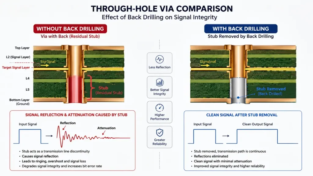
Through-Hole Via Comparison — Impact of Back Drilling on Signal Integrity
The via stub is one of the most consistently damaging structures in high-speed PCB design. When a through-hole via carries a signal from layer 1 to layer 8 in a 16-layer board, the lower portion of the via barrel (layers 9 through 16) is not part of the signal path. That unused length acts as a resonant stub that creates nulls in the frequency response at specific frequencies determined by the stub length.
At PCIe Gen 5 data rates (32 GT/s, fundamental frequency around 16 GHz), a stub as short as 0.8mm can create a transmission null that falls within the signal bandwidth and collapses the eye diagram. The 2026 solution is back-drilling: after the board is laminated and drilled, a second controlled-depth drilling operation removes the stub by boring out the unused via barrel from the opposite side. Back-drilling adds cost and lead time, but it is less expensive than the alternative — using blind vias for every high-speed signal, which requires additional sequential lamination press cycles.
Via-in-Pad Design and Conductive Fill Requirements for Advanced PCB Assemblies
Via-in-pad is a high-density design technique in which component pads and vias share the same footprint, eliminating the trace between pad and via and reducing the total footprint area. It is standard practice on BGA packages with pitches below 0.8mm and is increasingly required on 0.65mm and 0.5mm pitch AI processor packages.
The manufacturing requirement for via-in-pad is reliable conductive or non-conductive fill followed by planarization to create a flat, solderable surface. Inconsistent fill — partial voids, incomplete copper capping — leads to solder joint defects during reflow and is a known reliability risk in thermal cycling environments. Our 2026 via-in-pad process uses copper-filled and capped microvias with vertical interconnect continuity verified by cross-section analysis sampling before shipment on impedance-controlled production orders.
DFM Rules for Via Optimization: Aspect Ratio, Spacing, and Stack Configuration
The aspect ratio of a via — the ratio of drill depth to drill diameter — is the primary determinant of reliable copper plating in the barrel. The industry guideline for reliable plating is an aspect ratio at or below 10:1. A 1.6mm board with a 0.15mm drill has an aspect ratio of approximately 10.7:1, which is at the edge of what can be reliably plated with uniform copper wall thickness. At higher ratios, the electroplating bath cannot adequately circulate inside the hole, and thin spots in the copper barrel become fatigue initiation sites under thermal cycling.
For microvia (laser-drilled) structures, the standard 2026 capability at Hongda is 100µm diameter laser via with a depth-to-diameter ratio at or below 1:1. Stacked microvia structures — where three or more microvias are aligned vertically through sequential build-up layers — carry additional reliability risk at the interfaces between layers and should be validated against IPC-6012 Class 3 requirements for critical applications.
Through-hole via spacing to adjacent copper should maintain a minimum 0.1mm clearance beyond the anti-pad edge to prevent solder wicking during assembly. Designs that stack multiple layers of vias should alternate via positions between adjacent layers (staggered, not stacked) unless the design specifically requires stacked microvias for density.
Differential Pair Routing Rules for High-Speed PCB Manufacturing: Spacing, Impedance, and Length Matching
Differential signaling is the dominant interconnect paradigm for high-speed digital interfaces in 2026. PCIe, USB4, HDMI 2.1, DisplayPort 2.1, 100G/400G Ethernet SerDes, and MIPI standards all use differential pairs as the fundamental signal transport mechanism. The electrical advantage — common-mode noise rejection, doubled voltage swing for the same supply voltage — comes with precise manufacturing and routing requirements.
Differential Pair Impedance Control in PCB Fabrication
Differential pair impedance — typically 85Ω, 90Ω, 100Ω, or 120Ω depending on the interface standard — is a function of trace width, the gap between the two conductors, the dielectric thickness between the trace layer and the adjacent reference plane, and the dielectric constant of the PCB laminate material.
The 2026 PCB manufacturing environment offers significantly improved impedance control tolerances compared to five years ago. Hongda’s standard production tolerance for controlled-impedance traces is ±10%, with a premium tighter-tolerance process available at ±5% for microwave and phased-array antenna boards. The practical implication for designers: specify the target differential impedance on the fabrication drawing and coordinate with the manufacturer to confirm the stackup parameters will achieve it before routing begins.
Laminate material selection is central to impedance stability. Standard FR-4 laminates have a dielectric constant that varies with frequency and temperature. At 10 GHz, the Dk of standard FR-4 can shift by 15–20% compared to the 1 MHz reference value used in most material datasheets. High-speed designs routing at 25+ Gbps SerDes use low-loss laminates — materials such as Megtron 6, Isola I-Tera MT40, or Rogers 4350B — that maintain stable Dk and low dissipation factor (Df) at operating frequencies.
Common Differential Pair Routing Conflicts and DFM Solutions for High-Density PCBs
The most common routing conflict for differential pairs occurs when length-matching requirements push the designer toward serpentine (accordion) routing in dense areas of the board. Length matching ensures that the positive and negative members of a differential pair arrive at the receiver within a specified time window; the standard tolerance for PCIe Gen 5 is ±0.15mm intra-pair skew. Achieving this on a complex 24-layer board with multiple layer transitions often requires inserting meandered trace segments.
The DFM problem: serpentine sections that are too tightly spaced (where the straight segments are closer to each other than the coupling distance) create intra-pair crosstalk and degrade the noise rejection that differential signaling is supposed to provide. The 2026 routing guideline is to maintain a spacing between parallel segments of the meander equal to at least three times the trace width. A 100µm wide trace meander should have at least 300µm between parallel segments.
Layer transitions for differential pairs require matched vias: both the positive and negative conductors must transition through vias of identical geometry, placed symmetrically with respect to the pair centerline. Asymmetric via placement introduces skew and converts a portion of the differential signal to common mode, degrading EMI performance. This is a detail that automated via-placement tools often handle incorrectly and that requires manual verification in the design review.
Routing differential pairs across layer transitions also introduces the reference plane discontinuity problem. If the positive conductor transitions from a microstrip layer (with an adjacent ground plane on one side) to a stripline layer (with ground planes on both sides), and the negative conductor does not make the same transition simultaneously, the two conductors experience different electromagnetic environments for a portion of the routing — introducing skew and common-mode conversion. The DFM rule: always transition both members of a differential pair at the same point, using adjacent via structures.
Minimum Trace Width and Spacing for Differential Pairs in 2026 PCB Fabrication
The minimum manufacturable trace dimensions for differential pairs in controlled-impedance designs are constrained by both the impedance target and the fabrication process capability. For a standard 100Ω differential impedance on a stripline layer in a 0.2mm thick dielectric, typical trace dimensions are 100–120µm width with 100–150µm intra-pair gap. These dimensions are within the standard production capability of advanced PCB manufacturers in 2026 but require careful control of the etching process to maintain uniform width along the trace length.
Designers who tighten these dimensions to achieve higher routing density should verify that the resulting impedance still falls within the ±10% tolerance window before committing to the layout. A 10µm over-etch on a 100µm trace produces a 90µm trace, which shifts a 100Ω target to approximately 106Ω — still within tolerance. The same 10µm over-etch on a 75µm target trace shifts impedance to approximately 110Ω, outside the ±10% window.
2026 PCB Manufacturing Technology: What’s New and What Matters for Procurement
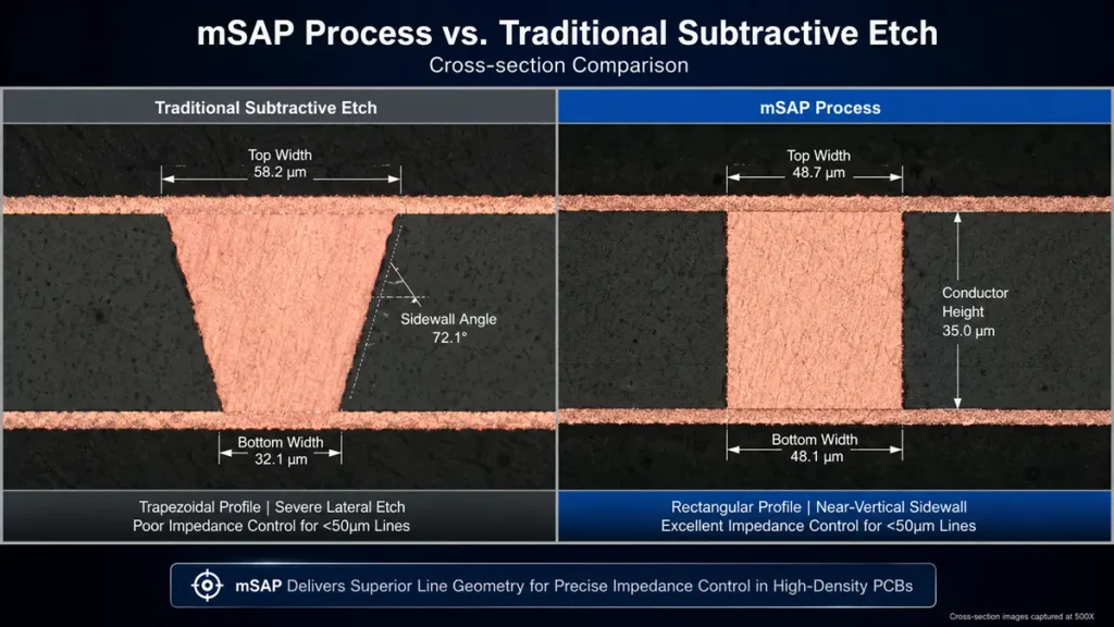
500X Cross-Section Comparison — mSAP Process vs. Traditional Subtractive Etch
The PCB industry has seen meaningful process capability advances enter volume production in 2026. Understanding these advances helps engineering and procurement teams identify which suppliers have invested in current-generation equipment and which are shipping boards on older baseline processes.
MSAP (modified Semi-Additive Process) for fine line production is now available from a growing number of Asia-Pacific manufacturers including Hongda. mSAP enables trace widths below 50µm with tighter dimensional control than subtractive etch, making it the enabling process for smartphone-class SLP boards and advanced AI chip carrier substrates entering the industrial and telecom PCB space.
Laser direct imaging (LDI) has largely replaced traditional photoplot and contact printing for inner layers on controlled-impedance boards. LDI eliminates the dimensional variation introduced by film handling and contact pressure, improving layer-to-layer registration by 30–50% compared to contact printing. This improvement directly reduces microvia misregistration risk in HDI stackups.
In-process impedance verification using time-domain reflectometry (TDR) on production coupons is standard practice at Hongda for all controlled-impedance orders. Coupon TDR data is included in the First Article Inspection report provided with each production lot.
AI-assisted DFM review tools have been integrated into Hongda’s engineering workflow, enabling faster turnaround on complex multi-layer designs and flagging potential manufacturing conflicts — such as via aspect ratio violations, annular ring deficiencies, and differential pair impedance mismatches — before the job enters the production queue.
Manufacturing-Friendly High-Speed PCB Design Rule Summary
The following condensed checklist reflects Hongda’s 2026 manufacturing guidance for high-speed PCB design teams. A complete version is available on request from our engineering team.
For trace geometry, design all controlled-impedance traces with a minimum 20% margin above the facility’s stated minimum width. Verify impedance calculations with the actual stackup, not a generic EDA library stackup, before routing begins.
For via design, keep through-hole via aspect ratios at or below 10:1. Specify back-drilling for all through-hole vias carrying signals above 10 Gbps when those vias do not use the full board thickness. Use via-in-pad only with conductive fill and copper capping, and confirm the fill process with the fabrication facility before tape-out.
For differential pair routing, always route both members of a pair on the same layer for the entire signal path except at planned layer transitions. Maintain consistent intra-pair gap throughout the routing, including through layer transitions. Keep serpentine meander segment spacing at three times trace width or greater. Match via geometry for positive and negative conductors at every layer transition point.
For stackup design, validate the stackup with the fabrication facility before beginning detailed routing. Confirm laminate material Dk and Df values at operating frequency, not at 1 MHz. For AI server and 400G networking designs, specify low-loss laminate materials and document material acceptance criteria in the purchase specification.
For DFM collaboration, submit designs for a formal DFM review before Gerber release. A DFM review adds one to two business days at the front end of a project and reliably eliminates the three to five business day respins that result from fabrication conflicts discovered after the job enters production.
FAQs:
How do I verify that a PCB manufacturer can actually deliver the impedance tolerance my high-speed design requires?
Request the manufacturer’s TDR measurement capability documentation and ask for sample TDR coupon reports from a recent production lot with comparable layer count and trace geometry. A credible advanced manufacturer will provide actual TDR data with the First Article Inspection package, not just a statement that they offer controlled impedance. Hongda provides coupon TDR data as standard documentation for all impedance-controlled orders, with measurements traceable to the IPC-2141A and IPC-6012 standards.
What PCB manufacturing certifications should I require for aerospace, medical, or defense applications?
The baseline certifications for safety-critical PCB applications are IPC-6012 Class 3 (performance specification for rigid printed boards), UL 94V-0 for flammability, and ISO 9001:2015 for quality management system. For military and aerospace procurement, AS9100D certification and adherence to IPC-A-600 Class 3 acceptability standards are typically required. Medical device PCBs should be manufactured by suppliers with ISO 13485 certification. Shenzhen Hongda Circuit Technology Co., Ltd. holds IPC, UL, ISO 9001:2015, and IATF 16949 certifications and can supply documentation packages meeting AS9100D requirements on request.
What information does a PCB supplier need to provide an accurate quote for a high-speed, multi-layer board?
A complete quotation package for a high-speed PCB should include Gerber RS-274X files or ODB++ data for all layers, a board outline drawing with tolerance, a drill file with finished hole size specifications, a stackup specification with dielectric material call-out and target layer thicknesses, controlled impedance requirements with target values and tolerances referenced to specific trace layers, surface finish specification (ENIG, HASL, OSP, etc.), IPC class requirement, quantity and delivery schedule, and any special requirements such as back-drilling, conductive via fill, or embedded components. Incomplete packages — particularly missing stackup specifications or unresolved impedance targets — are the primary cause of quotation delays and post-order engineering queries.
What is a realistic lead time for a prototype run of a 20-layer high-speed PCB with controlled impedance and back-drilling in 2026?
Standard prototype lead time for a 20-layer controlled-impedance board with back-drilling at Hongda is 10–14 working days from receipt of approved fabrication data and order confirmation. Expedited service for 7-working-day delivery is available on a capacity-confirmed basis with a surcharge. Lead times for production quantities (50+ panels) range from 15 to 25 working days depending on order complexity and current factory loading. Note that board designs requiring sequential lamination for blind and buried via structures, or designs using specialty low-loss laminates that require material procurement lead time, may require additional days.
How should I evaluate the DFM review process of a PCB supplier before placing a production order?
A supplier’s DFM review capability is one of the most important indicators of how well the production partnership will function. When evaluating a new supplier, ask for a sample DFM review report from a comparable board design. The report should identify specific issues (with layer, coordinate, and rule reference) rather than generic statements, provide recommended remedies for each flagged item, and include a response turnaround time commitment. At Hongda, our DFM review process covers trace width and spacing versus process capability, via aspect ratios and microvia stack configurations, differential pair routing consistency, impedance target verification against the submitted stackup, annular ring compliance, solder mask bridge capability for fine-pitch components, and panel utilization efficiency. The DFM report is delivered within 24 hours for standard designs and 48 hours for designs above 16 layers or with specialty requirements.
Shenzhen Hongda Circuit Technology Co., Ltd. is a certified PCB manufacturer specializing in high-density interconnect (HDI), controlled-impedance, and multi-layer rigid PCB fabrication for high-speed digital, RF, and mixed-signal applications. To request a DFM review, fabrication capability overview, or quotation, contact our engineering team through our official website. Email: pcb@pcbkr.com
About Author
David Chen https://www.linkedin.com/in/pcbcoming
David Chen boasts an extensive professional background in PCBA manufacturing, PCBA testing, and PCBA optimization, with specialized expertise in high-precision PCBA fault analysis and rigorous PCBA reliability testing. The author has worked with high-layer-count server PCB fabrication, ultra-low-loss backplane stackups, and thermo-mechanical reliability optimization for AI infrastructure projects involving 112G and 224G PAM4 architectures. Skilled in complex circuit design and cutting-edge advanced PCB manufacturing processes, he delivers solutions that elevate product durability and performance across industrial applications. His technical articles focusing on PCBA manufacturing workflows and testing methodologies are widely cited by industry peers, research institutions, and technical platforms, solidifying his reputation as a recognized technical authority in the global circuit board manufacturing sector.