Copper Base PCB for Power Electronics: Thermal Engineering for High-Power Systems
Copper Base PCB for Power Electronic.How copper substrate PCB manages junction temperature, thermal cycling, and current density across switching power supplies, IGBT/SiC modules, motor drives, renewable inverters, EV charging, and industrial lighting.
Copper Base PCB for Power Electronic delivers core thermal and mechanical advantages to address the rising power density challenges seen in industrial drives, renewable inverters, and EV charging hardware. The printed circuit board mounted under an IGBT or SiC module often determines if the power module can operate reliably through its full rated duty cycle. Shenzhen Hongda Circuit Technology Co., Ltd. manufactures copper base PCB and copper substrate PCB specifically to solve this pain point: these specialized boards rapidly dissipate heat from switching components, maintaining junction temperature, solder joints and dielectric layers within safe operating limits for long-term service.
This guide walks through why copper base PCB outperforms aluminum core and standard FR4 in power electronics, what has changed in copper substrate PCB manufacturing heading into 2026, and what a sourcing team needs to have ready before requesting a quote.
Why Power Electronics Rely on Copper Base PCB Instead of Aluminum or FR4
IGBTs, MOSFETs, and SiC power modules concentrate enormous current through a small silicon footprint. That concentration turns into heat almost instantly under load, and if the board under the device can’t carry that heat away, the junction temperature climbs until the part derates itself or fails outright.
Thermal Conductivity Gap Between Copper Base PCB and Aluminum Base PCB
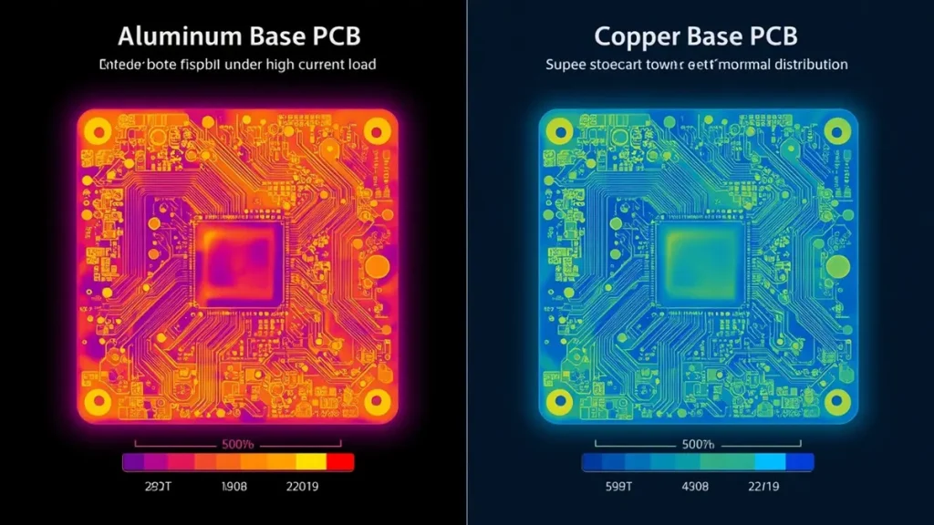
Thermal Conductivity Comparison: Aluminum Base PCB vs. Copper Base PCB
Copper’s thermal conductivity sits well above aluminum’s, and it clears standard FR4 by an order of magnitude. For a power converter running at continuous high current, that difference shows up directly as lower baseplate temperature and a wider safety margin before thermal shutdown.
Mechanical Load Capacity for Heavy Components and High-Current Layouts
Beyond heat, copper base PCB gives designers a substrate stiff enough to hold heavier connectors, bus bars, and press-fit components without the board flexing under vibration or thermal cycling — a common failure point in motor drives and traction inverters.
Thermal Diffusion and Power Stability: What Copper Substrate PCB Actually Buys You
The engineering payoff isn’t just “runs cooler.” It changes the failure curve of the whole assembly.
Junction Temperature Control and Device Lifespan
Faster thermal diffusion caps how high the junction temperature rises during a load transient. Since semiconductor lifetime scales inversely with peak junction temperature, even a modest drop compounds into meaningfully longer service life for the power module.
Reducing Thermal Gradients to Prevent Solder Fatigue and Delamination
Lower thermal resistance keeps electrical performance stable under sustained load, and a flatter thermal gradient across the board reduces the cyclic stress that drives solder joint fatigue and layer delamination. In a high-power inverter, improving thermal diffusion has been shown to cut hot-spot temperature by roughly 15–25%, which translates directly into fewer field failures over the warranty period.
2026 Manufacturing Advances in Copper Base PCB Production
Copper base PCB fabrication has moved past simple metal-core lamination. Several process refinements are now standard practice among specialized manufacturers.
Direct Bonded Copper and Active Metal Brazing Refinements
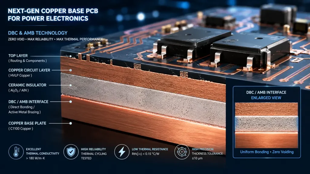
Cross-Section Stack-up of Next-Gen Copper Base PCB Featuring DBC & AMB Technology with Zero Voiding
Direct Bonded Copper (DBC) and Active Metal Brazing (AMB) ceramic substrates continue to tighten bond-layer uniformity, reducing voiding at the copper-ceramic interface and improving thermal cycling endurance for SiC and GaN power modules operating at higher switching frequencies.
Laser-Drilled Microvias and Copper Inlay for High-Current Density
Laser-drilled microvias paired with copper inlay or coin technology let designers route direct thermal paths under the power device itself, rather than relying solely on lateral heat spreading — a meaningful step up for compact, high-current-density layouts.
Simulation-Driven Design for Manufacturability Review
Thermal simulation tools now run earlier in the design cycle, flagging hot-spot risk and copper balance issues before the first prototype panel is even fabricated. Pairing this with a formal DFM review shortens the iteration loop between stack-up design and first-article inspection.
Typical Applications for Copper Base PCB in Power Electronics
Copper base PCB shows up wherever a design pushes high current through a compact footprint and can’t tolerate a weak thermal path. The six categories below cover most of the real-world sourcing requests we see for copper substrate PCB.
Switching Power Supplies and Industrial Power Converters
Switch-mode power supplies and industrial power converters run their rectification and switching stages at high frequency, and every switching transition generates a heat pulse concentrated right at the MOSFET or diode footprint. In a PSU rated for continuous industrial duty, a copper base PCB keeps the baseplate temperature stable across load swings, which matters more than peak efficiency numbers once the unit is running 24/7 in a cabinet with limited airflow. Designers working on AC-DC front ends, DC-DC converters, and industrial power modules typically specify copper base thickness alongside dielectric thermal conductivity as a matched pair, not as independent variables, since undersizing either one shows up as thermal derating on the datasheet.
IGBT and Silicon Carbide (SiC) Power Modules
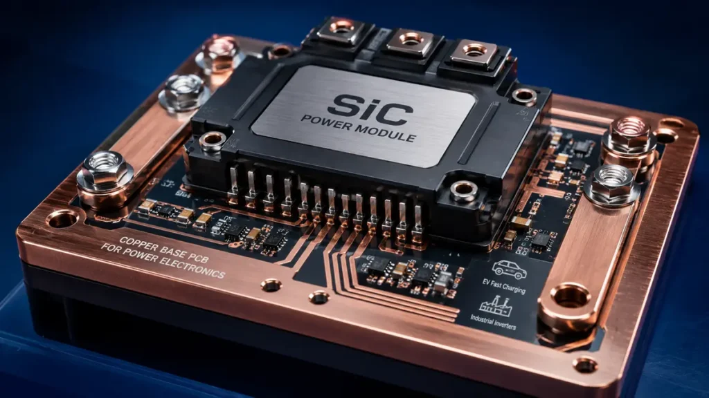
Premium Silicon Carbide (SiC) Power Module Integrated on Thick Copper Base PCB
IGBT and SiC modules are the clearest case for copper base PCB or DBC/AMB copper-ceramic substrates, because the die itself has almost no thermal mass to buffer a current spike. SiC modules in particular switch faster than silicon IGBTs, which pushes switching losses into shorter, sharper thermal events. A copper substrate PCB with a direct thermal path — copper inlay or thermal via array positioned directly under the die — pulls that heat out before it raises junction temperature enough to shorten the module’s service life. This is also where DBC and AMB process refinements matter most, since bond-layer voiding at the copper-ceramic interface directly limits how many thermal cycles the module survives.
Motor Drives and Servo Control Systems
Motor drive and servo control boards combine high-current switching stages with dense control circuitry on the same board, often in a housing with no active cooling beyond a heat sink bolted to the copper base. Servo systems in particular see frequent direction reversals and load transients, which cycle the thermal load up and down constantly rather than holding it steady — exactly the pattern that drives solder joint fatigue if the board’s thermal gradient isn’t well controlled. Copper base PCB gives these designs the mechanical stiffness to mount heavier connectors and current sensors as well as the thermal path to survive the duty cycle.
Renewable Energy Inverters: Solar and Wind
Solar string inverters and wind turbine power converters operate outdoors or in enclosures exposed to wide ambient temperature swings, and they’re expected to run for a warranty period measured in decades, not years. That combination — variable ambient conditions plus a very long service life requirement — makes thermal margin a reliability question as much as a performance one. Copper base PCB in these inverters supports the IGBT or SiC switching stage while also tolerating the thermal cycling that comes from daily sun exposure or fluctuating wind loads, which is why inverter manufacturers tend to specify thicker copper base layers than an indoor industrial converter would need.
EV Charging Systems and Onboard Power Modules
DC fast chargers and onboard EV power modules push very high current through connectors, bus bars, and switching stages packed into a housing with strict size and weight targets. Copper base PCB handles both sides of that constraint: it carries the current density without excessive trace heating, and it moves heat to the enclosure fast enough to keep the charging session running at rated power rather than throttling down. Onboard modules add vibration and mechanical shock to the requirement list, which is another reason copper base substrates are preferred over lighter alternatives that can’t hold up mechanically under automotive duty cycles.
High-Current LED Drivers and Industrial Lighting Power Boards
High-current LED drivers and industrial lighting power supplies are a lower-voltage application, but the current density at the driver IC and output stage still generates concentrated heat in a small footprint, especially in dimmable or high-output fixtures. Copper base PCB in this application is less about extreme thermal cycling and more about maintaining consistent LED drive current and preventing thermal derating that shows up as flicker or reduced output over the fixture’s lifetime — a common complaint with underspecified aluminum-base alternatives in high-current lighting designs.
Structural Design Considerations for Copper Base PCB Manufacturing
Copper Base Thickness and Circuit Copper Foil Selection
Base thickness is set by the thermal load the application generates, while circuit-layer copper foil thickness is sized for the current the traces need to carry without excessive resistive heating.
Dielectric Layer Selection for Maximum Thermal Conductivity
The dielectric layer should be as thin as the design allows while still meeting isolation voltage requirements, since dielectric thickness is usually the single largest contributor to overall thermal resistance. Thermal vias or direct bonding zones placed under the power device shorten this path further.
Surface Finish: ENIG or OSP for Power Modules
Surface finish selection — ENIG or OSP — depends on assembly process and long-term reliability requirements. Layout should also account for wide trace widths, even current distribution, and adequate creepage distance for high-voltage sections.
Common Failure Modes in Copper Substrate PCB and How They’re Mitigated
| Failure Mode | Root Cause | Mitigation |
| Thermal delamination | CTE mismatch between layers | Optimized dielectric material, controlled lamination process |
| Solder joint fatigue | Repeated thermal cycling | Improved heat spreading, refined pad geometry |
| Component failure at hot spots | Uneven copper distribution | Balanced copper fill, engineered thermal path |
| Dielectric breakdown | Insufficient dielectric strength under high voltage | Higher dielectric-strength material selection |
| Warpage affecting assembly | Unbalanced copper and base thickness | Controlled copper balance and base thickness |
How to Select a Copper Base PCB Manufacturer: A Sourcing Guide
Start with power density and thermal load requirements for the target application.- Select copper foil thickness based on current rating and mechanical strength needed.
- Weigh thermal conductivity against dielectric thickness — this trade-off shapes total thermal resistance.
- Match the PCB structure to the cooling method: air cooling, liquid cooling, or heat-sink integration.
- Confirm the manufacturer can document compliance with relevant standards, including industrial safety requirements and RoHS.
Requesting a Copper Base PCB Quote from Shenzhen Hongda Circuit Technology
Parameters to Include in Your RFQ
- Rated power and current load
- Board dimensions and layer stack-up
- Thermal performance targets (thermal resistance, maximum operating temperature)
- Copper layer thickness and base thickness
- Application context (inverter, power supply, motor drive, etc.)
- Compliance requirements, including RoHS, REACH, and UL certification where applicable
Next Steps: Gerber Submission and DFM Review
Submit Gerber files along with stack-up requirements, request thermal simulation support and a DFM review, and expect a quote turnaround within 24–48 hours.
Frequently Asked Questions: Sourcing a Copper Base PCB Supplier
What should I look for when comparing copper base PCB manufacturers on Google?
Check whether the supplier publishes real thermal resistance data and stack-up options rather than generic marketing copy, confirm they support DFM review and thermal simulation before tooling, and look for documented certifications (ISO 9001, UL, IATF 16949 for automotive work) rather than unverified claims.
What’s the difference between copper base PCB and aluminum base PCB for power applications?
Copper base PCB offers substantially higher thermal conductivity and greater mechanical rigidity than aluminum base PCB, making it the stronger choice for high-current power modules, though it typically comes at a higher material cost and added board weight.
Can a copper base PCB manufacturer support small-batch prototyping before mass production?
Most established manufacturers, including Shenzhen Hongda Circuit Technology, offer prototype runs with the same stack-up and copper thickness intended for production, which lets engineering teams validate thermal performance before committing to volume tooling.
What lead time should a buyer expect for a custom copper base PCB order?
Quote turnaround is typically 24–48 hours once Gerber files and stack-up requirements are submitted; actual production lead time depends on copper thickness, layer count, and whether DBC/AMB processing is required, so it’s worth confirming both quote and production timelines separately.
Do copper base PCB suppliers in China meet RoHS, REACH, and UL requirements for export markets?
Reputable manufacturers maintain documentation for RoHS, REACH, and relevant UL certifications and will provide compliance paperwork on request — buyers sourcing for EU or North American end markets should ask for this documentation before finalizing an order rather than assuming it by default.
About Author
David Chen https://www.linkedin.com/in/pcbcoming
David Chen boasts an extensive professional background in PCBA manufacturing, PCBA testing, and PCBA optimization, with specialized expertise in high-precision PCBA fault analysis and rigorous PCBA reliability testing. The author has worked with high-layer-count server PCB fabrication, ultra-low-loss backplane stackups, and thermo-mechanical reliability optimization for AI infrastructure projects involving 112G and 224G PAM4 architectures. Skilled in complex circuit design and cutting-edge advanced PCB manufacturing processes, he delivers solutions that elevate product durability and performance across industrial applications. His technical articles focusing on PCBA manufacturing workflows and testing methodologies are widely cited by industry peers, research institutions, and technical platforms, solidifying his reputation as a recognized technical authority in the global circuit board manufacturing sector.