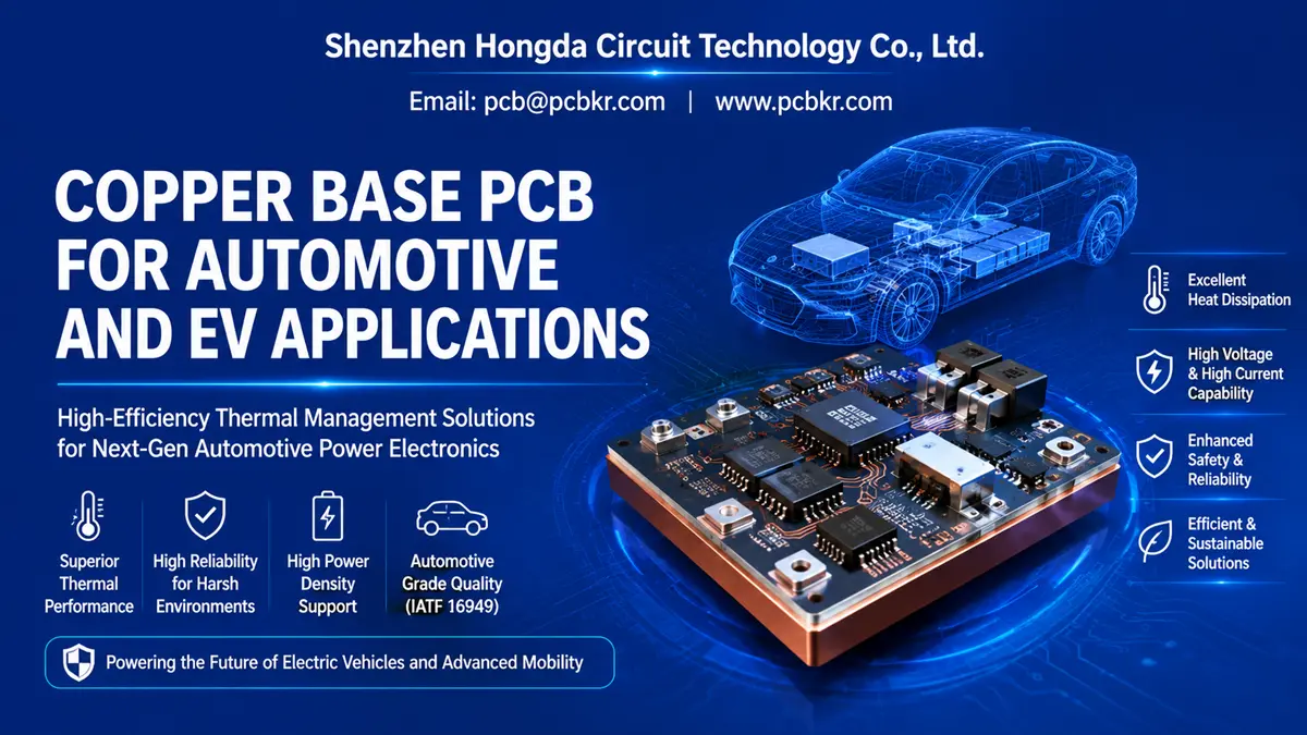
Copper Base PCB for Automotive and EV Applications
High-Efficiency Thermal Management Solutions for Next-Gen Automotive Power Electronics
Shenzhen Hongda Circuit Technology Co., Ltd
Copper Base PCB for Automotive and EV Applications is pivotal amid the profound transformation of modern automotive electronic architectures, driven by the rapid transition toward electric vehicles (EVs) and advanced driver-assistance systems (ADAS). As operating currents surge and electronic package sizes continue to shrink, traditional FR4 substrates are increasingly incapable of dissipating critical thermal loads generated by high-performance automotive electronic systems. Against this backdrop, sourcing high-reliability thermal substrates has evolved into a fundamental safety priority for global Tier 1 automotive suppliers and original equipment manufacturers (OEMs) to guarantee the stable and safe operation of EV and ADAS devices.
This technical deep dive breaks down design logic, material performance, automotive validation standards, and manufacturing innovations of high thermal conductivity copper base PCBs built for harsh EV power electronics environments.
Why Automotive & EV Electronics Require Superior Thermal Stability
Modern electric drivetrains operate under extreme electrical stress, demanding thermal performance far beyond standard industrial circuit boards.
The Thermal Burden of High Power Density EV PCBs
EV powertrains rely on wide-bandgap semiconductors (SiC, GaN) installed inside traction inverters, onboard chargers (OBC), and Battery Management Systems (BMS). These power components generate concentrated local heat. Without effective heat dissipation via specialized metal-core PCBs, semiconductor junction temperatures quickly exceed safe limits, triggering mechanical stress, gate oxide failure, and irreversible system breakdown.
Thermal Runaway Prevention & Functional Safety Compliance
High-voltage battery packs and Power Distribution Units (PDUs) suffer heat buildup with inadequate cooling. Excess heat damages dielectric insulation, creates microcracks in solder joints, and raises thermal runaway risks. Stable thermal performance directly safeguards ASIL C/D rated vehicle safety systems, making copper base substrates a non-negotiable reliability component.
FR4 & Aluminum IMS vs. Copper Base PCB Thermal Performance
Standard FR4 thermal conductivity sits at only 0.25 W/m·K. Conventional aluminum insulated metal substrates (IMS) deliver 1.0–3.0 W/m·K. Automotive-grade copper base PCBs feature pure copper cores with thermal conductivity up to 400 W/m·K. This massive thermal jump cuts thermal resistance drastically, lowers chip junction temperatures, and extends semiconductor service life.
Hongda Manufacturing Advantage
Shenzhen Hongda Circuit Technology uses multi-stage vacuum lamination equipment to produce void-free heavy copper and metal-base PCB structures. Precision pressure and temperature control guarantee uniform dielectric bonding on high-conductivity copper cores.
Core Automotive & EV Use Cases for Copper Base PCBs
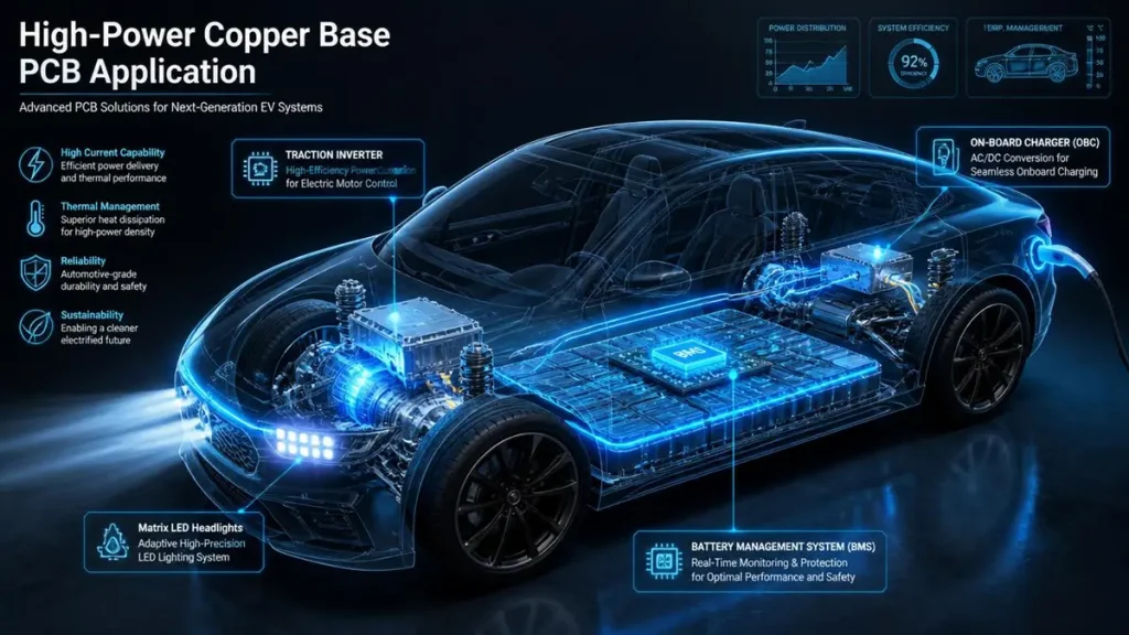
Primary Applications of High-Power Copper Base PCBs in Next-Generation EV Powertrains and Electronic Control Units
Copper core circuit boards serve mission-critical, high-current, high-heat vehicle subsystems:
- EV Traction Inverters & Motor Control Units (MCU) High-frequency switching creates heavy heat losses. Copper base substrates deliver fast vertical and horizontal heat transfer to boost energy conversion efficiency.
- On-Board Chargers (OBC) & DC-DC Converters High-voltage AC-DC conversion generates sustained thermal load; thick copper traces support extreme continuous current flow.
- Battery Management Systems (BMS) Manages hundreds of lithium-ion cells with precision monitoring. Copper base backing provides rigid mechanical support and cooling for monitoring ICs and high-current balance resistors.
- Power Distribution Units (PDU) Heavy copper conductive paths carry hundreds of amps across the full vehicle power network.
- Adaptive Matrix LED Headlights Compact high-power LED arrays create concentrated hotspots. Metal core PCBs stabilize light output and prevent LED color shift or premature burnout.
- ADAS & Autonomous Driving Compute Modules High-speed processors for lidar, radar, and camera data require efficient cooling inside sealed, zero-ventilation enclosures.
Strict Automotive Environmental & Reliability Standards
Automotive PCB specifications far outpace commercial electronics with rigid operating limits:
Wide Temperature Cycle Endurance
Vehicle power electronics must reliably operate from -40°C to +150°C. Standard FR4 suffers severe Z-axis thermal expansion that damages copper vias. Qualified automotive copper base PCBs maintain structural integrity through over 1,000 thermal shock cycles, complying with IPC-TM-650 and JESD22 testing standards.
Shock & Vibration Mechanical Resistance
Continuous road vibration and sudden impact loads are standard vehicle operating conditions. Per ISO 16750 requirements, copper base PCBs adopt high-tensile copper alloys and specialized resin dielectrics to absorb mechanical shock, eliminating trace and solder joint micro-fractures.
Harsh Environment Chemical Protection
Road salt, constant humidity, and industrial chemical contaminants demand robust surface protection. Automotive copper base boards use premium surface finishes, flawless solder masks, and high-adhesion conformal coatings for long-term corrosion resistance.
Critical Performance Benchmarks: FR4 vs Aluminum IMS vs Hongda Copper Base PCB
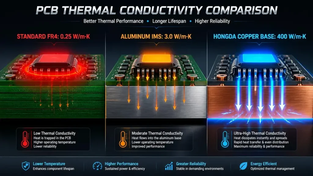
Thermal Conductivity Comparison between Standard FR4, Aluminum IMS, and Hongda Advanced Copper Base PCB
| Performance Metric | Standard FR4 Substrate | Aluminum IMS Substrate | Hongda Advanced Copper Base PCB |
|---|---|---|---|
| Thermal Conductivity (W/m·K) | 0.20 – 0.35 | 1.0 – 3.0 | 200 – 400 (Direct Bonding Structure) |
| X/Y CTE Thermal Expansion | 14 – 17 ppm/K | 22 – 24 ppm/K (High ceramic stress) | 16 – 17 ppm/K (Perfect copper trace matching) |
| Dielectric Breakdown Voltage | >40 kV | 2 – 6 kV | Up to 10 kV (Ultra-thin high-performance dielectric resin) |
| Maximum Continuous Current | Low (<20A) | Moderate (20A – 80A) | Extreme (>200A) with heavy copper traces |
Ultra-Low Thermal Resistance + High Dielectric Strength
We deploy ultra-thin (50µm) thermally conductive insulating (TCI) dielectric layers. These substrates achieve minimal thermal resistance while supporting >8kV AC breakdown voltage, combining efficient heat transfer and high-voltage isolation.
CTE Matching Eliminates Thermal Delamination
Copper base core CTE (16.5 ppm/K) nearly matches copper circuit traces (17 ppm/K). This alignment eliminates shear stress during thermal cycling, solving the common delamination failure seen in aluminum IMS boards.
Automotive-Grade Surface Finishes for SMT Assembly
We offer mass-production compatible surface finishes for automated SMT assembly:
- ENIG (Electroless Nickel Immersion Gold)
- OSP (Organic Solderability Preservative)
- Immersion Silver
These finishes block copper oxidation and maintain flat co-planarity for fine-pitch power device soldering.
High-Power PCB Layout Design & Engineering Guidelines
Automotive high-power circuit design requires strict DFM rules and high-voltage electrical safety compliance.
Optimized Stack-Up & Direct Copper Bonding (DCB)
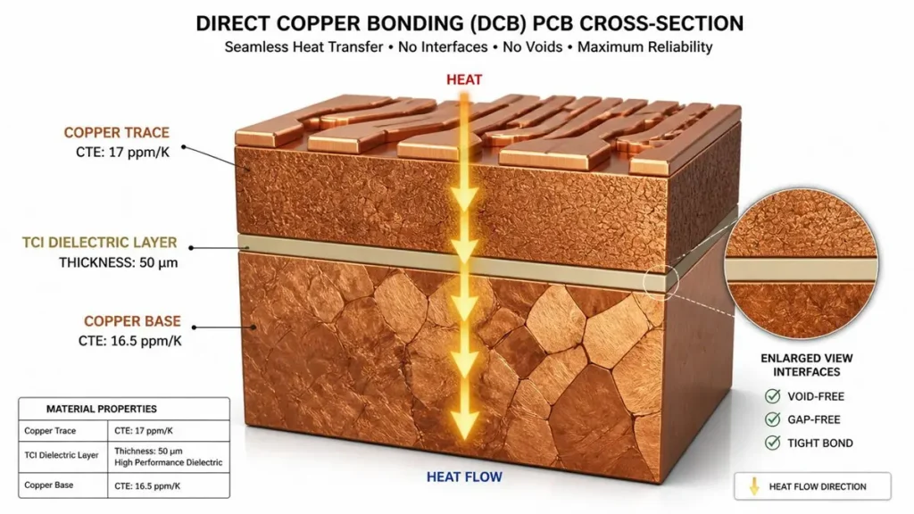
Microscopic 3D Cross-Section of Hongda Direct Copper Bonding (DCB) Structure with Perfect CTE Matching
Standard insulated metal substrates rely on a polymer barrier between circuit copper and metal base. For high-density power components, we apply Direct Copper Bonding (DCB) and thermocompression bonding. This technology bonds copper traces directly to the copper core, removing the polymer thermal barrier and driving thermal resistance close to zero.
High-Voltage Clearance, Creepage & Isolation Safety
EV platforms operate at 400V up to 800V systems. To prevent arcing and electrical tracking, layouts must follow IEC 60664 creepage and clearance rules. Our engineering team optimizes edge spacing and separates high-voltage traces from grounded copper base layers to eliminate isolation risks.
FEA Thermal Simulation Pre-Production Validation
Before manufacturing, our engineers run full Finite Element Analysis (FEA) thermal simulation:
- Identify potential hotspots under maximum current loads
- Map complete heat dissipation pathways
- Verify mechanical layout meets target service life
Precision Fabrication Equipment
Our workflow uses LPKF Laser Direct Structuring (LDS) and Schmoll high-precision drilling machines. Sub-micron accuracy enables microvia fabrication and custom mechanical cavities for complex multi-layer copper base PCB designs.
Automotive-Grade Quality Testing & Validation Protocols
Zero-defect long-term field reliability requires comprehensive destructive and non-destructive testing:
- Thermal Shock & Power Cycling Test Environmental chambers cycle boards between -40°C and +150°C to validate dielectric adhesion and detect copper trace micro-fractures.
- HTOL High-Temperature Operating Life Test Boards run at full electrical/thermal load for up to 1,000 hours, simulating 15 years of real-world vehicle operation.
- 100% Automated Hi-Pot Dielectric Testing Every finished board undergoes high-voltage isolation inspection to eliminate pinholes and micro-voids in dielectric insulation.
- Microsection Cross-Section Analysis Destructive slice testing under high-magnification microscopy verifies metal grain structure, copper thickness, and lamination interface integrity.
Mandatory Supplier Capabilities for Automotive Copper Base PCBs
Supplying Tier 1 auto manufacturers demands certified production systems and specialized manufacturing technology.
IATF 16949 Certified Production
Shenzhen Hongda Circuit holds full IATF 16949 automotive quality certification. Our quality system includes:
- Full end-to-end material batch traceability
- Complete PPAP production part approval workflows
- Real-time SPC statistical process control for all manufacturing stages
Advanced Heavy Copper & Lamination Technology
Metal core and heavy copper PCB production requires precise etching and registration control. Our automated horizontal etching lines support copper thickness up to 6 oz (210µm), delivering low resistance traces and consistent impedance control.
Full MES Production Traceability
Every automotive PCB receives a unique laser-engraved 2D barcode linked to our Manufacturing Execution System (MES). Data records include raw material batches, production shift logs, vacuum lamination parameters, and AOI inspection results for full audit traceability.
Inspection Equipment Investment
Our facility runs Orbotech LDI laser direct imaging and dual-sided automated optical inspection (AOI) systems. High-resolution trace scanning achieves 100% automated inspection of fine line/spacing copper base substrates.
OEM & Tier 1 Bulk Procurement Guidance
Procurement teams must balance performance, cost, and stable supply chain delivery:
Cost vs. Total System Performance Tradeoff
Copper base PCBs carry higher upfront material costs than aluminum IMS, but superior thermal performance removes bulky external heat sinks and liquid cooling assemblies. This reduces overall vehicle weight and cuts total system manufacturing costs.
Stable Supply Chain & Lead Time Control
Long-term raw material partnerships and high-capacity automated production lines guarantee consistent delivery timelines for mass automotive production volumes.
Custom Co-Engineering Support
Our engineering team collaborates directly with customer design teams to optimize board dimensions, surface finishes, and stack-up configurations, balancing performance targets and cost budgets.
Why Copper Base PCBs Are The Standard For Next-Gen EV Power Systems
Integrating heavy copper metal-core substrates into automotive power designs delivers three core competitive advantages:
- Class-Leading Thermal Dissipation Direct heat evacuation from power semiconductors eliminates thermal throttling and extends component operational lifespan.
- Superior Mechanical & Electrical Reliability CTE-matched copper cores paired with high-performance resin dielectrics prevent laminate separation and solder joint fatigue during thousands of thermal cycles.
- Reduced Vehicle Weight & Compact Packaging Eliminating large passive heat sinks shrinks power converter footprint and lowers overall vehicle weight, directly improving EV driving range.
For Tier 1 automotive suppliers upgrading power electronic hardware, partnering with a specialized IATF 16949 copper base PCB manufacturer is critical. Shenzhen Hongda Circuit Technology combines dedicated thermal substrate manufacturing equipment, strict automotive quality control, and specialized thermal design expertise to deliver high-reliability thermal management boards for next-generation electric vehicles.
Buyer FAQ: Sourcing Automotive Copper Base PCBs
How does Shenzhen Hongda Circuit Technology guarantee void-free lamination in heavy copper
and metal-clad PCBs?
We deploy high-precision vacuum lamination presses operating under <10 mbar vacuum with optimized heat and pressure cycles, fully removing air bubbles and micro-voids from insulating resin layers.
Every batch undergoes 100% automated C-SAM scanning acoustic microscopy sampling plus cross-section microimaging to confirm full resin fill around thick copper traces and uniform bonding.
What dielectric materials support 800V high-voltage EV architectures with high thermal conductivity?
We supply ultra-thin polymer-ceramic filled dielectric sheets ranging from 50µm to 150µm, with thermal conductivity between 3.0 W/m·K and 8.0 W/m·K. These materials deliver high dielectric strength, sustaining over 8kV AC breakdown voltage for safe isolation in 800V EV drivetrains.
Can your factory fabricate heavy copper traces up to 6oz+? What DFM rules apply for thick copper layers?
Yes, we specialize in metal-core heavy copper PCBs supporting trace thickness up to 10 oz. Minimum line width/spacing DFM requirements for thick copper:
3 oz copper: 8mil line / 10mil space minimum
6 oz copper: 15mil line / 18mil space minimum Our engineering team reviews all customer layouts pre-production to optimize trace spacing and ensure stable etching yields.
How do you maintain full traceability and change control under IATF 16949 automotive standards?
The entire production line is tracked by MES manufacturing execution software. Each PCB carries a serialized unique 2D laser barcode linked to raw material batches, AOI inspection logs, and vacuum press process parameters.
We follow formal PPAP protocols; all material, process, or tooling modifications require formal customer approval before implementation.
What are your standard lead times for copper base PCB prototypes vs mass automotive production?
1. Expedited engineering prototypes: 7–10 working days (includes full DFM review + thermal dielectric testing)
2. Standard mass production orders: 3–4 weeks Lead times shift slightly based on copper thickness and raw material availability. We maintain safety stock of specialized copper laminates to stabilize delivery schedules for high-volume automotive programs.
About Author
David Chen https://www.linkedin.com/in/pcbcoming
David Chen boasts an extensive professional background in PCBA manufacturing, PCBA testing, and PCBA optimization, with specialized expertise in high-precision PCBA fault analysis and rigorous PCBA reliability testing. The author has worked with high-layer-count server PCB fabrication, ultra-low-loss backplane stackups, and thermo-mechanical reliability optimization for AI infrastructure projects involving 112G and 224G PAM4 architectures. Skilled in complex circuit design and cutting-edge advanced PCB manufacturing processes, he delivers solutions that elevate product durability and performance across industrial applications. His technical articles focusing on PCBA manufacturing workflows and testing methodologies are widely cited by industry peers, research institutions, and technical platforms, solidifying his reputation as a recognized technical authority in the global circuit board manufacturing sector.