Copper Base PCB Thermal Performance Guide: How Advanced Manufacturing Drives Better Heat Dissipation
Copper Base PCB Thermal Performance Guide: Power density keeps climbing in LED lighting, motor drives, and industrial power electronics, and the printed circuit board is often where a design either survives that heat or fails under it. This guide focuses on copper base PCB, also known as metal core PCB (MCPCB), which delivers engineers a direct, low-resistance heat conduction channel to draw heat away from active components, preventing junction temperature from becoming the bottleneck of product performance.
At Shenzhen Hongda Circuit Technology Co., Ltd., our production lines combine thick-copper electroplating, precision laser via drilling, and in-house thermal simulation to turn that theoretical advantage into a board that performs consistently in real tests, matching datasheet thermal indicators.
This complete guide covers PCB thermal performance definitions, copper base heat conduction principles, key design variables, power density-based structural selection, thermal testing methods, and actionable design tips for high-power hardware projects.
1. What Is Thermal Performance and Thermal Management in PCB Design
1.1 Core Concept & Key Thermal Indicators
Thermal performance describes how effectively a board structure transfers heat from electronic components to the surrounding environment. Thermal management refers to systematic design optimization that controls heat flow, adjusting materials, layout and stacking structure to keep chip junction temperature within safe operating ranges during long-term operation.
The core objectives of PCB thermal management:
- Guarantee long-term device reliability
- Lower semiconductor junction temperature (Tj) relative to ambient temperature (Ta)
- Stabilize electrical performance throughout the product service life
Engineers rely on these standard thermal metrics for evaluation:
- Power density: Heat generation per unit board area
- Junction temperature (Tj) & Ambient temperature (Ta)
- Thermal resistance: θJA (junction-to-ambient), θJC (junction-to-case), unit: °C/W
- Heat flux: Thermal energy flow rate passing through a fixed cross-section
1.2 Board-Level vs System-Level Thermal Management
Thermal optimization includes two inseparable dimensions:
- Board-level thermal management: Determines the baseline thermal resistance via copper thickness, thermal via density, dielectric thickness and substrate material. This is the foundation of all heat dissipation design.
- System-level thermal management: Depends on external conditions such as enclosure airflow, heatsink fitting and ambient temperature range.
Key rule: Even high-performance cooling systems cannot avoid component thermal runaway if the PCB substrate itself has high thermal resistance. A copper base PCB must be designed with both board and system cooling boundaries in mind.
2. How Copper Base PCBs Improve Heat Dissipation Efficiency
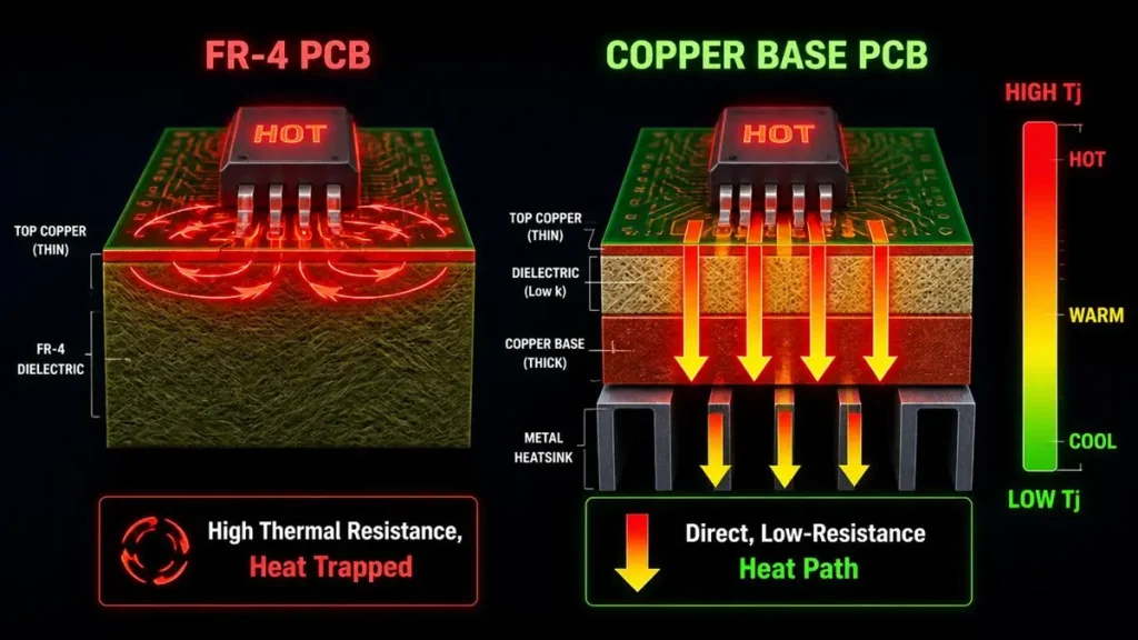
Thermal Performance Comparison: Copper Base PCB vs FR-4
2.1 Basic Stack-up Structure of Copper Base MCPCB
A copper base PCB replaces standard FR-4 core with a solid copper metal substrate, bonded to circuit layers through thermally conductive dielectric. The standard three-layer stack-up:
- Conductor copper layer: SMD soldering area, copper weight ranges from 1oz to heavy copper 10oz
- Thermally conductive dielectric insulation layer: Provides electrical isolation while minimizing thermal resistance
- Solid copper base plate: Acts as integrated heat spreader to eliminate local hot spots
2.2 Copper Base PCB vs Traditional FR-4
Copper thermal conductivity is nearly two orders of magnitude higher than standard FR-4 laminate. FR-4 boards trap heat near chips and only rely on surface copper traces and air convection for cooling; copper base substrates create a continuous low-resistance vertical heat conduction path straight to heatsinks or chassis.
Core advantages of copper base PCB:
- Lower overall junction-to-case thermal resistance
- Short, direct vertical heat conduction instead of weak lateral spreading only
- Uniform temperature distribution on dense high-power boards
2.3 Typical Application Scenarios
Copper base metal core boards are widely used for equipment with sustained high current and high heat output:
- High-power LED lighting modules
- Industrial motor drives
- Power converter electronics
- Solid-state relays & solar power optimizers
3. Heat Conduction Pathways and Structural Relationships
3.1 Standard Heat Transfer Route
Heat follows a fixed multi-layer conduction path on copper base PCB: Component Chip → Thermal Pad / Land Pattern → Conductive Dielectric Interface → Copper Base Plate → Thermal Interface Material (TIM) → External Heatsink / Chassis / Ambient Air
3.2 Layer Structure Impacts Thermal Resistance
Every layer in the stack creates thermal resistance. Three critical structural factors:
- Dielectric thickness & thermal conductivity: Thinner, high-k dielectric is the most effective way to cut vertical thermal resistance
- Conductor copper thickness: Thick copper foil expands heat spreading area under power chips to avoid thermal bottlenecks
- Copper base plate thickness: Thicker copper substrate provides thermal capacitance to absorb transient temperature spikes
3.3 Interfacial Contact Thermal Resistance
Air voids between contact surfaces become natural thermal insulators. Solder joints, thermal adhesive and TIM layers all introduce contact resistance. Poor solder wetting or voids inside bonding layers will completely offset the heat dissipation advantages of copper base substrates. Uniform mechanical pressure and high-performance thermal interface materials are required to eliminate air gaps.
3.4 Lateral vs Vertical Heat Conduction
PCB heat dissipation relies on two heat transfer modes:
- Lateral (in-plane) spreading: Copper base plate evenly distributes heat across the board surface
- Vertical (through-plane) conduction: Thermal vias and dielectric layers transfer heat downward to the metal base
Qualified thermal layout balances both modes instead of relying on a single heat transfer path.
4. Key Variables That Affect PCB Thermal Performance
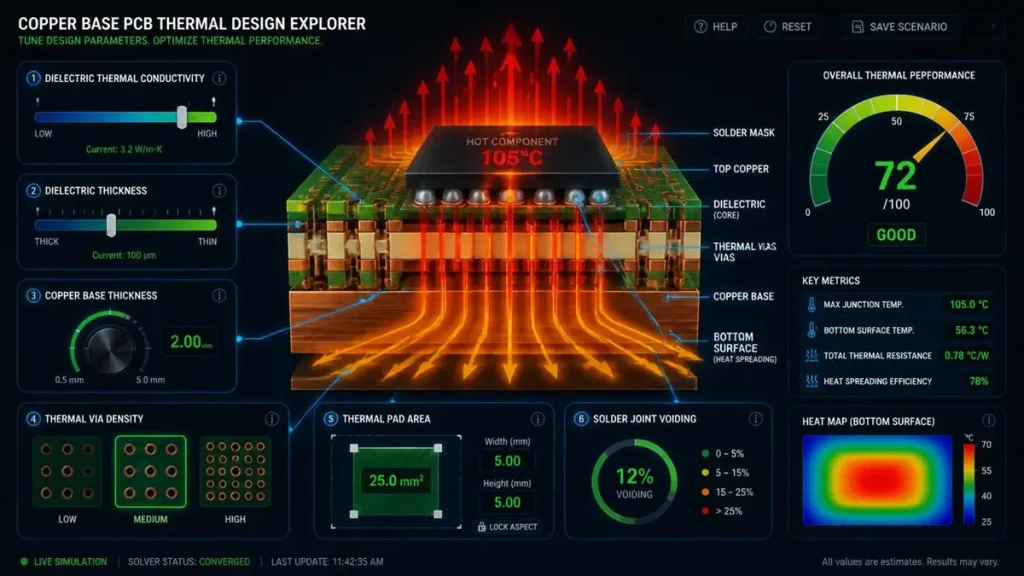
Interactive PCB Thermal Performance Simulation Dashboard
Five categories of factors determine the final thermal performance of copper base PCB:
- Material parameters Copper base thickness, dielectric thermal conductivity & thickness, solder alloy thermal characteristics. These values define the minimum thermal resistance the board can achieve and the maximum sustainable power density.
- Geometry & layout design Component spacing density, thermal pad size, thermal via quantity, via diameter and filling method. Reasonable layout reduces thermal coupling between heat sources and eliminates concentrated hot spots.
- Power load characteristics Local power density, steady-state continuous power vs transient pulse power. Transient power spikes bring greater thermal stress to dielectric and bonding interfaces.
- Manufacturing tolerance & interface quality Copper thickness uniformity, void-free dielectric lamination, surface flatness. Voids inside dielectric or solder pads form micro hot spots and easily trigger dielectric breakdown under long-term operation.
- Environmental boundary conditions Natural convection vs forced air cooling, ambient temperature range, heatsink mounting pressure. These conditions decide the maximum heat the whole system can dissipate.
5. How to Select PCB Structure Based on Power Density
We classify designs by power density to avoid over-engineering or insufficient cooling performance.
5.1 Power Density Classification
- Low power density: Heat load can be fully dissipated by natural air convection, no concentrated hot spots, standard FR4 or thin copper core is acceptable
- Medium power density: Requires thick copper foil, dense thermal via arrays and thin high-conductivity dielectric to enhance lateral heat spreading
- High power density: Needs copper base metal core, ultra-thin high-k dielectric and filled thermal vias to build direct vertical heat conduction channels
5.2 Optional Copper Base PCB Structures
- Single-sided copper MCPCB: Cost-effective for high-power LED and general industrial equipment
- Double-sided / Multilayer copper base PCB: For complex signal routing on both sides of substrate, with insulated thermal vias connecting layers
- DBC / AMB ceramic copper substrate: High-end solution for extreme power electronics, supporting high voltage and repeated thermal cycling
5.3 Core Design Trade-offs: Thermal Performance vs Cost & Manufacturability
Thicker copper base and ultra-thin dielectric reduce thermal resistance but bring obvious drawbacks:
- CTE mismatch between copper, dielectric and chips leads to solder joint fatigue and dielectric delamination during thermal cycling
- Heavy copper base requires special CNC machining, raising production costs
Professional PCB manufacturers can provide DFM review to optimize stacking structure and balance cooling performance with manufacturing cost.
6. Testing and Validation Methods for Thermal Performance
Thermal design cannot be finalized without real measurement verification. Standard testing and validation solutions include:
6.1 Core Test Indicators
Thermal resistance θJA/θJC measurement, junction temperature testing, full board surface temperature mapping.
6.2 Common Test Equipment & Methods
- Infrared thermal imaging: Capture full surface temperature distribution to locate hot spots
- Thermocouple / thermistor point temperature measurement
- Transient thermal impedance spectroscopy: Detect high-resistance interfaces inside stacking layers
- 3D X-Ray inspection: Analyze void rate inside power component solder joints
6.3 Board & System Level Reliability Verification
- Steady-state thermal testing & power cycling test
- Accelerated aging & thermal shock test (-40℃ ~ +125℃)
- Wind tunnel cooling fixture test to simulate real airflow environment
6.4 Standard Test Data Management Rules
Record complete operating conditions, ambient temperature and measurement uncertainty for all test data, to ensure comparability between different design revisions.
7. Practical Design Recommendations for Copper Base PCB Thermal Management
7.1 Standard Thermal Design Workflow
- Clarify core requirements: Power density, operating ambient temperature, target junction temperature Tj
- Select matching copper thickness, dielectric material and substrate stacking structure
- Run thermal simulation to predict chip temperature and hot spot distribution
- Manufacture prototype samples and complete physical thermal testing
- Optimize layout or stacking structure according to test data before mass production
7.2 Layout Optimization Tips
- Expand thermal pad area under high-power semiconductor devices
- Separate heat-generating components to avoid heat superposition hot zones
- Add more, larger filled thermal vias to strengthen vertical heat conduction
- Match copper foil thickness and dielectric thermal conductivity to actual power load
- Improve thermal interface material selection and heatsink mechanical contact pressure
7.3 Manufacturing Coordination Suggestions
Complete DFM review with PCB manufacturers in advance to confirm copper thickness tolerance, thermal via filling process and dielectric lamination quality. All thermal performance verification must be finished on prototype samples before mass production.
How Shenzhen Hongda Circuit Technology Supports Thermal-Critical PCB Manufacturing
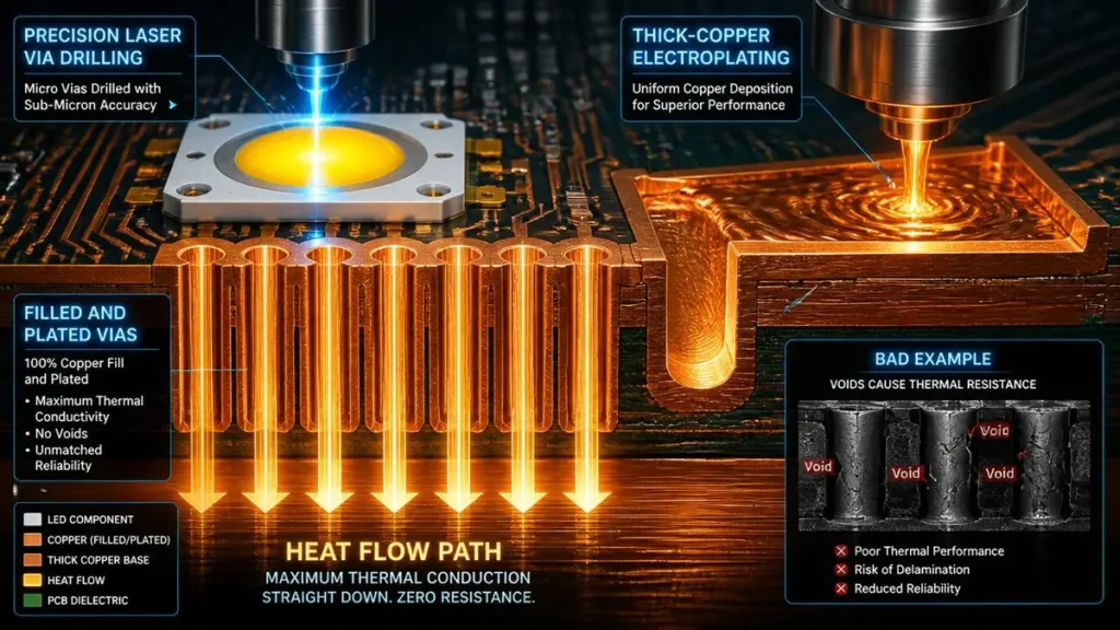
Advanced Copper Base PCB Manufacturing Processes
From thermal simulation to mass-produced copper base PCB, stable thermal performance relies on precise manufacturing process control. Our factory provides full-process support for high-heat-dissipation metal core boards:
- Thick-copper electroplating production lines: Uniform copper deposition for high-current, high thermal conductivity circuit layers
- Precision laser via drilling: Custom diameter dense thermal vias, filled & plated vias for maximum vertical heat transfer
- Full inspection system: AOI automated optical inspection + X-Ray void detection to eliminate bonding defects before delivery
- Early DFM engineering review: Optimize stacking, copper weight and via layout according to thermal requirements before quotation
- Prototype thermal measurement service: Test real θJA / θJC thermal resistance data on physical samples instead of relying solely on simulation
This complete process control ensures the measured thermal resistance of finished copper base PCB matches design simulation values, effectively avoiding field failures of high-power electronic products caused by insufficient heat dissipation.
FAQ for PCB Buyers & Hardware Engineers
What key standards should I check when selecting a copper base PCB manufacturer?
Ignore simple marketing slogans and focus on verifiable process capabilities: copper thickness processing range, optional dielectric thermal conductivity grades, thermal via filling capacity, and whether the supplier provides free DFM review before quotation. Valid certifications include ISO 9001, IATF 16949 (automotive industry) and UL certification for LED products. Sample lead time is also an important screening factor.
How to compare thermal performance data between different PCB suppliers?
Ask suppliers to provide actual tested θJA/θJC data under unified standard test conditions, not only raw material thermal conductivity parameters. Even with identical dielectric materials, thermal resistance differs greatly due to via layout, copper thickness and lamination void rate. Request physical samples for side-by-side thermal testing for accurate comparison.
What is the core difference between metal core MCPCB and standard FR4 PCB with thermal vias?
Metal core PCB replaces the base substrate with high-conductivity copper plate connected by continuous conductive dielectric, forming a full-board low-resistance heat transfer channel. FR4 boards with thermal vias only improve local vertical heat conduction around via arrays, without upgrading the overall low thermal conductivity of epoxy substrate. High-power products require copper base MCPCB; medium-low power designs can adopt FR4 with dense thermal vias as a cost-saving alternative.
Can manufacturers assist with thermal stacking design, or do I need to finalize the structure before quotation?
Experienced copper base PCB suppliers can provide thermal design suggestions during DFM review. Provide your power density, component layout and target junction temperature requirements, and our engineers will recommend copper thickness, dielectric grade and thermal via layout plans. You do not need fully fixed stacking layers to request quotations.
How long is the prototype lead time for thermally validated copper base PCB samples?
Lead time depends on copper thickness and thermal via complexity. Factories with self-owned thick copper plating and laser drilling equipment (no outsourced processing) deliver prototypes faster with fewer process errors. We provide customized sample delivery cycles based on your specific stacking structure.
About Author
David Chen https://www.linkedin.com/in/pcbcoming
David Chen boasts an extensive professional background in PCBA manufacturing, PCBA testing, and PCBA optimization, with specialized expertise in high-precision PCBA fault analysis and rigorous PCBA reliability testing. The author has worked with high-layer-count server PCB fabrication, ultra-low-loss backplane stackups, and thermo-mechanical reliability optimization for AI infrastructure projects involving 112G and 224G PAM4 architectures. Skilled in complex circuit design and cutting-edge advanced PCB manufacturing processes, he delivers solutions that elevate product durability and performance across industrial applications. His technical articles focusing on PCBA manufacturing workflows and testing methodologies are widely cited by industry peers, research institutions, and technical platforms, solidifying his reputation as a recognized technical authority in the global circuit board manufacturing sector.