Blind Via PCB Cost Guide: Price Breakdown, Cost Drivers & Money-Saving Tips
Introduction: Why Blind Via PCB Pricing Demands Strategic Understanding
Blind via technology sits at the intersection of performance necessity and cost sensitivity. Every procurement manager who has requested an HDI PCB quote has faced the same question: why does adding a few laser-drilled vias multiply the board cost by two, three, or even five times? To understand total cost of ownership across full stackups, review our complete cost and manufacturing guide for blind & buried via PCBs.
The answer lies not in markup, but in physics and process engineering. A standard 8-layer through-hole board requires one lamination cycle, one drilling pass, and one plating sequence. An equivalent 2+N+2 HDI board with blind vias demands five lamination cycles, three drilling passes (two laser, one mechanical), and three plating sequences. The raw processing time stretches by a factor of 3.2x, which maps directly to a 2.5–3.5x price multiplier after accounting for material costs and yield loss.
At Shenzhen Hongda Circuit Technology Co., Ltd., we have manufactured blind via PCBs across every industry tier—from consumer wearables to NVIDIA Blackwell-class AI server substrates. This guide draws from our actual 2026 production data, material costs, and process economics to give you a transparent, actionable understanding of blind via PCB pricing. You will learn exactly where costs originate, how to optimize your design for manufacturability, and how to distinguish genuine value from inflated quotes.
Whether you are budgeting a prototype run or negotiating a 10,000-unit production contract, the insights here will sharpen your procurement strategy and protect your margins.
Average Blind Via PCB Cost: 2026 Price Ranges by Board Type and Volume
Blind Via PCB Price Comparison Across Complexity Tiers
Blind via PCB pricing does not follow a linear scale. Each additional process step—laser drilling, sequential lamination, via filling—compounds rather than adds to the base cost. The following table reflects actual Q3 2026 pricing from Shenzhen-based HDI manufacturers, FOB Shenzhen, for standard 100mm × 100mm boards:
| PCB Type | Construction | Prototype (5–10 pcs) | Low Volume (100 pcs) | Production (1,000+ pcs) |
|---|---|---|---|---|
| Standard Multilayer | 8L, through-hole only | $350–$600 | $30–$75 | $8–$18 |
| Blind Via PCB | 8L, 1+N+1 HDI | $800–$1,500 | $40–$100 | $12–$35 |
| Blind & Buried Via PCB | 10L, 2+N+2 HDI | $1,200–$2,500 | $60–$150 | $20–$50 |
| Advanced HDI PCB | 12L, 3+N+3 stacked | $2,000–$4,000 | $100–$250 | $35–$80 |
| Any Layer HDI | 16L, ELIC (Every Layer Interconnect) | $3,500–$7,000 | $200–$400 | $60–$120 |
Source: AtlasPCB 2026 China PCB Manufacturing Pricing Guide
Prototype vs. NPI vs. Mass Production Blind Via PCB Cost
The cost curve for blind via PCBs is steep at low volumes and flattens significantly at scale. Understanding where you sit on this curve determines your negotiation leverage:
- Prototype quantities (5–10 units): Fixed tooling costs dominate. Laser drilling programs, test fixture fabrication, and engineering review represent 40–60% of the total quote. Expect $800–$1,500 per board for a basic 1+N+1 HDI prototype.
- NPI quantities (50–200 units): Variable material and process costs begin to dominate, but setup fees still inflate per-unit pricing. Typical range: $40–$150 per board depending on complexity.
- Mass production (1,000+ units): Economies of scale kick in aggressively. Material purchasing power, optimized panel utilization, and streamlined process flows can reduce per-unit costs by 60–70% compared to prototype pricing. A board that costs $1,200 in prototype drops to $12–$35 at 1,000-unit volume.
Why Blind Via PCB Prototype Cost Is Disproportionately High
Prototype pricing shocks many first-time HDI buyers. A typical mid-capability PCB fabrication facility carries approximately $122,000 in fixed monthly operating expenses before producing a single board. These costs—equipment depreciation, cleanroom climate control, wastewater treatment compliance, and engineering salaries—are recovered through setup and tooling fees on low-volume orders. When you order 5 prototype boards, you are effectively subsidizing the entire facility’s fixed cost base across those 5 units.
The 10 Biggest Factors Affecting Blind Via PCB Manufacturing Cost
Laser Drilling Cost — The Primary Cost Driver in Blind Via PCB Fabrication
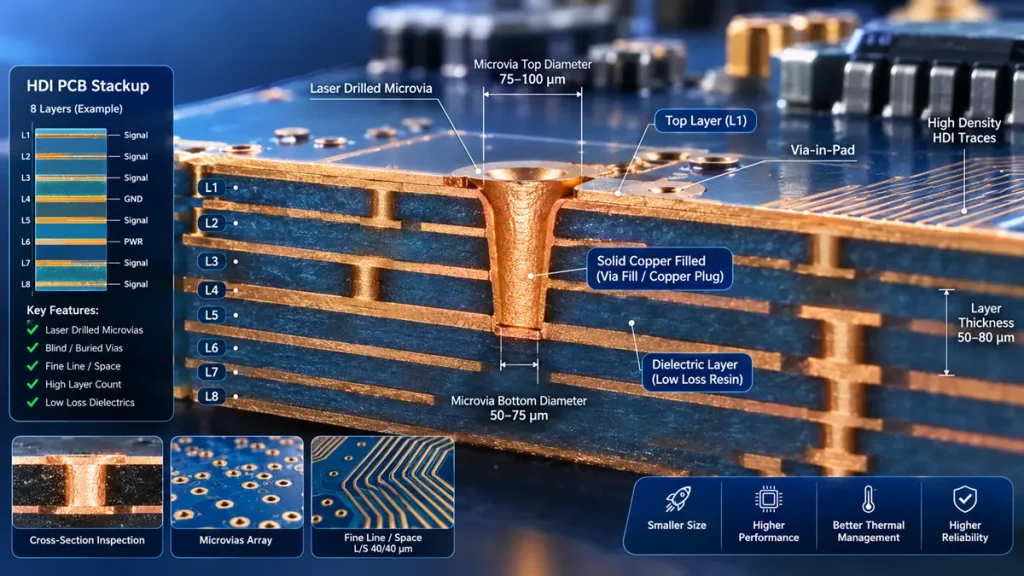
3D isometric cutaway diagram of an 8-layer HDI PCB stackup detailing laser-drilled blind via dimensions, layer-by-layer buildup (L1–L8), and electroplated solid copper filling structure.
Laser drilling is the single most expensive process step unique to blind via manufacturing. A UV+CO2 hybrid laser system capable of 50μm microvias represents a capital investment of $800,000–$1,200,000 per machine. Amortized across production volume, this equipment cost translates directly to per-hole pricing.
Cost breakdown per laser-drilled blind via (2026 rates):
| Via Diameter | Standard FR-4 | High-Tg / Low-Loss | Notes |
|---|---|---|---|
| 100–150μm | $0.03–$0.05 | $0.05–$0.08 | Standard HDI range |
| 75–100μm | $0.05–$0.10 | $0.08–$0.15 | Fine-pitch BGA applications |
| 50–75μm | $0.10–$0.20 | $0.15–$0.30 | Advanced AI server microvias |
Variables affecting laser drilling cost:
- Hole quantity: Each additional 1,000 holes adds 15–25 minutes of machine time
- Material type: Low-loss laminates (Megtron 6/7, Rogers) require adjusted laser parameters and slower feed rates
- Registration accuracy: ±10μm accuracy demands dual-camera systems with real-time drift compensation—increasing cycle time by 20–30%
- Panel size: Larger panels allow more holes per loading cycle, reducing per-hole overhead
At Hongda Circuit, our 2026 equipment fleet includes femtosecond laser systems for next-generation glass substrate processing, enabling sub-50μm vias with zero thermal damage to surrounding dielectric.
Sequential Lamination Cost — Why Each Extra Press Cycle Multiplies Your Quote
Sequential lamination is the second-largest cost driver after laser drilling. Each lamination cycle requires five distinct process steps that standard multilayer fabrication does not:
- Laser via drilling — Separate program, separate pass for each buildup layer
- Desmear and seed layer deposition — Preparing blind via walls for plating
- Electrolytic copper fill or flash plating — Filling the vias
- Surface preparation for next lamination — Oxide treatment or alternative bonding enhancement
- Precision alignment lamination — Registration verification before pressing
Cost impact of sequential lamination cycles:
| Lamination Cycles | Process Time Multiplier | Price Multiplier (vs. Standard ML) | Typical Application |
|---|---|---|---|
| 1 cycle (standard ML) | 1.0x | 1.0x | Consumer electronics |
| 2 cycles (1+N+1) | 1.8x | 1.5–2.0x | Networking, industrial |
| 3 cycles (2+N+2 staggered) | 2.5x | 2.2–2.8x | Automotive, telecom |
| 4 cycles (2+N+2 stacked) | 3.2x | 2.8–3.5x | AI servers, medical |
| 5+ cycles (3+N+3 / ELIC) | 4.0x+ | 3.5–5.0x | Aerospace, military |
The raw processing time for a 2+N+2 HDI board is approximately 3.2x longer than an equivalent through-hole multilayer, which directly maps to the price multiplier after accounting for material costs and yield loss.
Via Filling Cost — Resin Filled vs. Copper Filled vs. VIPPO
Via filling transforms hollow vias into solid structures, enabling via-in-pad (VIP) designs and improving thermal/mechanical performance. The filling method you choose has a direct and significant impact on cost:
| Filling Method | Cost per Via (prototype) | Cost per Via (volume) | Thermal Performance | Best For |
|---|---|---|---|---|
| Resin Filled | $0.08 | $0.03–$0.05 | Moderate | Consumer, standard BGA |
| Conductive Filled | $0.12 | $0.05–$0.08 | Good | Power distribution |
| Copper Filled | $0.15–$0.25 | $0.08–$0.15 | Excellent | High-power, fine-pitch BGA |
| VIPPO (Via in Pad, Plated Over) | $0.20–$0.35 | $0.10–$0.20 | Excellent | AI server, high-density |
Key considerations:
- Resin filling is the default for most HDI applications. It provides adequate planarity for standard BGA pitches (0.8mm+) at the lowest cost.
- Copper filling adds 20–50% to via-related costs but delivers superior thermal conductivity and mechanical reliability. It is mandatory for fine-pitch BGA (0.4mm pitch) and high-current applications.
- VIPPO requires copper filling plus additional surface planarization steps, making it the most expensive option but essential for maximum density designs.
Hongda Circuit offers all four filling methods with vacuum-assisted processes that achieve <2% void content, verified by 3D X-ray CT inspection.
Material Cost — How Laminate Selection Drives 40–60% of Total Blind Via PCB Price
Material selection is the silent cost giant in blind via PCB manufacturing. While laser drilling and lamination grab attention, the laminate itself often represents the largest single cost component.
2026 material cost comparison (per square meter, 1.6mm thickness):
| Material Grade | Cost (USD/m²) | Tg (°C) | Df @10GHz | Typical Application |
|---|---|---|---|---|
| Standard FR-4 | $8–$12 | 130–140 | 0.020 | Consumer electronics |
| High-Tg FR-4 | $12–$18 | 170–180 | 0.018 | Automotive, industrial |
| Megtron 6 | $25–$40 | 180 | 0.002 | 10G/25G networking |
| Megtron 7 | $40–$60 | 200 | 0.001 | 56G/112G telecom |
| Megtron 8 / M9 | $60–$90 | 220 | 0.0008 | 224G AI server |
| Rogers 4350B | $80–$120 | — | 0.0037 | RF/microwave |
| Polyimide (Flex) | $50–$80 | — | 0.003 | Rigid-flex HDI |
The 2026 BOM crisis context: Industry data shows that net BOM costs for high-density systems have surged 25% to 40% compared to the latter half of 2025. Copper prices have exceeded $13,300/ton, and a structural shortage of low-CTE glass fiber fabric has created long lead times and quota systems. These constraints are independent—both must ease before significant laminate cost relief is likely.
Layer Count — The Non-Linear Cost Escalation in Blind Via PCB Manufacturing
Each additional layer in a blind via PCB does not add a fixed cost—it multiplies complexity across drilling, lamination, alignment, and testing.
Prices per board at 1,000-unit volume, 100×100mm, standard materials
| Layer Count | Standard ML Cost | 1+N+1 HDI Cost | 2+N+2 HDI Cost | Key Cost Driver |
|---|---|---|---|---|
| 4L | $2–$12 | N/A | N/A | Basic multilayer |
| 6L | $10–$25 | $25–$60 | N/A | First HDI capability |
| 8L | $30–$75 | $40–$100 | $60–$150 | Impedance control |
| 10L | $50–$120 | $80–$180 | $100–$250 | Sequential lamination |
| 12L | $80–$180 | $120–$280 | $150–$350 | Stacked vias |
| 16L | $150–$350 | $200–$450 | $250–$550 | ELIC consideration |
| 20L+ | $300–$600 | $400–$800 | $500–$1,000+ | Maximum complexity |
Trace Width and Space — mSAP and Fine Line Technology Cost Impact
Trace geometry directly determines which imaging and etching technologies a manufacturer must deploy:
| Trace/Space | Manufacturing Method | Cost Premium | Application |
|---|---|---|---|
| 6/6 mil (0.152mm) | Standard LDI | Baseline | General HDI |
| 4/4 mil (0.102mm) | Advanced LDI | +15–25% | Fine-pitch BGA |
| 3/3 mil (0.076mm) | mSAP (semi-additive) | +40–60% | High-density mobile |
| 2/2 mil (0.051mm) | SAP (fully additive) | +80–120% | Ultra-HDI, SiP |
mSAP (modified semi-additive process) is increasingly required for AI server PCBs routing 224Gbps signals. While it adds significant cost, it enables the 30μm line/space geometries necessary for dense BGA escape routing.
Hongda Circuit operates both LDI and mSAP lines, with production capability down to 30μm line/space on M9-grade substrates.
Surface Finish Cost — ENIG, ENEPIG, OSP, and Hard Gold Comparison
Surface finish selection affects both assembly compatibility and long-term reliability:
| Finish Type | Cost (per m²) | Shelf Life | Best For | Cost Impact |
|---|---|---|---|---|
| OSP | $2–$4 | 6 months | Consumer, cost-sensitive | Baseline |
| Immersion Tin | $4–$8 | 12 months | Press-fit connectors | +10–15% |
| ENIG | $8–$15 | 24 months | BGA, fine-pitch | +20–30% |
| ENEPIG | $12–$20 | 24+ months | Wire bonding, medical | +35–45% |
| Hard Gold | $25–$50 | 36+ months | Edge connectors, high-wear | +50–100% |
For blind via PCBs with via-in-pad designs, ENIG is the default choice due to its flat surface topography and excellent solderability. ENEPIG is increasingly specified for medical and aerospace applications requiring wire bonding capability.
Panel Utilization — The Hidden Cost Optimizer in Blind Via PCB Manufacturing
PCB raw material is sold by the sheet (typically 18” × 24” or 21” × 24”). Panel utilization—the percentage of panel area occupied by usable boards—directly impacts per-unit material cost.
| Panel Utilization | Material Waste | Cost Impact | Optimization Strategy |
|---|---|---|---|
| <50% | >50% | +40–60% vs. optimal | Redesign board outline |
| 50–65% | 35–50% | +15–25% vs. optimal | Adjust array configuration |
| 65–80% | 20–35% | Baseline | Standard array design |
| >80% | <20% | -10–15% vs. baseline | Custom panel optimization |
Hongda Circuit panel optimization services: Our engineering team reviews every new design for panel utilization before quoting. Simple adjustments—rounding corners, reducing board outline by 2mm, or rotating the array—can improve utilization by 15–20% without affecting electrical performance.
Testing Cost — AOI, Flying Probe, Fixture Test, X-Ray, and Cross Section
Blind via PCBs require more extensive testing than standard multilayer boards:
| Test Method | Cost per Panel | Purpose | When Required |
|---|---|---|---|
| AOI (Automated Optical Inspection) | $5–$15 | Surface defect detection | 100% of production |
| Flying Probe Test | $15–$40 | Electrical continuity | Prototype, low volume |
| Fixture Test (ICT) | $200–$800 setup + $2–$5/unit | High-speed electrical test | Volume production |
| X-Ray Inspection | $10–$30 | Void detection, alignment | HDI, stacked vias |
| Cross Section Analysis | $50–$150/sample | Microstructure validation | Qualification, FA |
| Impedance Test | $5–$15 | Controlled impedance verification | High-speed designs |
For a typical 1+N+1 HDI prototype lot, testing represents 15–25% of the total manufacturing cost. At volume, this drops to 5–10% as fixture test amortizes the setup cost.
Reliability Qualification Cost — Thermal Cycling, IST, and CAF Testing
High-reliability applications require additional qualification testing that adds significant cost to prototype and NPI builds:
| Qualification Test | Cost per Build | Lead Time | Required For |
|---|---|---|---|
| Thermal Cycling (500 cycles) | $300–$600 | 2–3 weeks | Automotive, industrial |
| Thermal Cycling (1000+ cycles) | $600–$1,200 | 4–6 weeks | Aerospace, medical |
| IST (Interconnect Stress Test) | $200–$400 | 1–2 weeks | Automotive (IATF 16949) |
| CAF Test (1000h) | $400–$800 | 6–8 weeks | High-voltage, dense designs |
| Humidity Bias (85/85, 1000h) | $300–$500 | 6–8 weeks | Automotive, marine |
| Full IPC Qualification Package | $1,500–$3,000 | 8–12 weeks | Class 3, military |
These costs are typically absorbed by the manufacturer for production orders but charged separately for prototype and qualification builds.
Blind Via PCB Cost Breakdown — Where Every Dollar Goes

3D data visualization breakdown of HDI blind via PCB manufacturing costs, highlighting key percentage allocations across raw materials, laser microvia drilling, sequential lamination, and quality testing.
Typical Cost Distribution in a 2+N+2 Blind Via PCB (1,000-unit volume)
The following table represents actual cost allocation from Hongda Circuit’s 2026 production analytics for a 10-layer, 2+N+2 HDI board with 100μm blind vias, Megtron 6 material, ENIG finish, and standard testing:
| Cost Component | Percentage | USD per Board | Notes |
|---|---|---|---|
| Raw Material ( laminate, copper foil, prepreg) | 28% | $14.00 | Megtron 6, 1.6mm, 1oz Cu |
| Sequential Lamination | 22% | $11.00 | 3 press cycles |
| Laser Drilling | 18% | $9.00 | 2,000 holes, UV+CO2 hybrid |
| Via Filling (Copper) | 12% | $6.00 | VIPPO, vacuum-assisted |
| Testing & Inspection | 8% | $4.00 | AOI, X-ray, flying probe |
| Surface Finish (ENIG) | 5% | $2.50 | 2μ” Au / 120μ” Ni |
| Engineering & CAM | 4% | $2.00 | DFM review, panelization |
| Scrap & Yield Loss | 2% | $1.00 | 95% first-pass yield |
| Packaging & Shipping | 1% | $0.50 | Vacuum seal, desiccant |
| Total | 100% | $50.00 |
Note: This represents a mid-range 2+N+2 HDI board. Costs scale significantly with material grade, layer count, and via density.
How Yield Loss Affects Blind Via PCB Fabrication Cost
Yield is the hidden variable that separates profitable HDI manufacturing from financial loss. A 5% yield improvement on a $50 board saves $2.50 per unit—at 10,000 units, that’s $25,000 in recovered margin.
Typical yield rates by HDI complexity (Hongda Circuit 2026 data):
| HDI Structure | First-Pass Yield | Rework Rate | Scrap Rate |
|---|---|---|---|
| 1+N+1 | 96–98% | 2–3% | <1% |
| 2+N+2 staggered | 92–95% | 4–6% | 1–2% |
| 2+N+2 stacked | 88–92% | 6–8% | 2–3% |
| 3+N+3 | 85–90% | 8–10% | 3–5% |
| ELIC / Any Layer | 80–85% | 10–12% | 5–7% |
Yield loss concentrates in three areas:
- Laser drilling misregistration — Most common in stacked via designs
- Plating voids in high-aspect-ratio vias — Especially in 3+N+3 and ELIC
- Delamination during sequential lamination — Material-dependent, worse with low-Tg laminates
Hongda Circuit’s investment in dual-camera fiducial alignment, vacuum-assisted filling, and real-time SPC monitoring maintains yield rates 3–5% above industry averages.
Blind Via PCB vs. Through Hole PCB Cost — A Complete Side-by-Side Comparison
Manufacturing Complexity and Cost Differential
| Comparison Factor | Through Hole PCB | Blind Via PCB | Cost Impact |
|---|---|---|---|
| Drilling method | Mechanical drill, one pass | UV+CO2 laser, multiple passes | +200–400% |
| Lamination cycles | 1 cycle | 2–5 cycles | +150–400% |
| Plating sequences | 1 sequence | 2–3 sequences | +100–100% |
| Layer registration | Standard alignment | Precision alignment (<±25μm) | +50–100% |
| Testing requirements | Basic electrical | AOI + X-ray + microsection | +100–150% |
| Material grade | Standard FR-4 | High-Tg / low-loss required | +50–200% |
| Design density | Moderate | Very high (BGA escape routing) | Enables smaller board size |
| Signal integrity | Limited by via stubs | Stub-free interconnects | Essential for >10Gbps |
| Overall cost ratio | 1.0x (baseline) | 2.5–5.0x |
When Blind Vias Actually Reduce Total Product Cost
Despite the 2.5–5x fabrication premium, blind vias can reduce total system cost in three scenarios:
- Board size reduction: A 6-layer blind via design often replaces an 8–10 layer through-hole board. The layer count reduction can offset the via premium while delivering a smaller, lighter product.
- Assembly cost savings: Via-in-pad eliminates the need for dog-bone fanout patterns, reducing board area by 20–30% and simplifying assembly.
- Performance-driven designs: In 224Gbps AI server backplanes, through-hole vias create unacceptable signal reflections. The blind via premium is non-negotiable—there is no cheaper alternative that meets the electrical specification.
Blind Via vs. Buried Via Cost Comparison — Which Is More Expensive and Why?
Cost Structure Analysis of Blind Vias vs. Buried Vias
| Cost Factor | Blind Via | Buried Via | Explanation |
|---|---|---|---|
| Drilling cost | Higher | Lower | Blind vias require precision laser drilling from the surface; buried vias are drilled during inner layer processing |
| Lamination cycles | Same | Same | Both require sequential lamination |
| Inspection cost | Higher | Lower | Blind vias can be X-rayed from the surface; buried vias require layer-by-layer verification or destructive testing |
| Rework feasibility | Possible | Nearly impossible | Blind via defects can sometimes be accessed; buried via defects scrap the entire board |
| Design flexibility | Higher | Lower | Blind vias connect surface to inner layers; buried vias only connect internal layers |
| Typical cost premium | Baseline | -10 to -20% | Buried vias are slightly cheaper but far less flexible |
Practical recommendation: Most cost-optimized HDI designs use a combination—blind vias for surface-to-layer connections and buried vias for internal routing. This hybrid approach balances cost with routing density.
HDI PCB Cost Comparison by Structure — 1+N+1 vs. 2+N+2 vs. 3+N+3 vs. Any Layer HDI
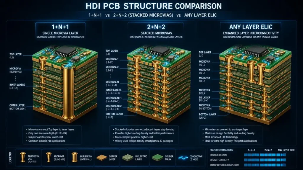
Comprehensive 3D cross-section comparison of HDI PCB buildup architectures (1+N+1, 2+N+2 with stacked microvias, and Any Layer ELIC), detailing microvia connections, routing density, and manufacturing complexity.
Price Scaling Across HDI Complexity Tiers
Source: AtlasPCB HDI Cost Breakdown 2026
| HDI Structure | Layer Count | Price Range (100pc, 50×50mm) | Price Range (1k vol., 100×100mm) | Key Cost Driver |
|---|---|---|---|---|
| 1+N+1 | 6–8L | $12–$35/unit | $12–$35/unit | 1 laser drill + 1 extra press |
| 2+N+2 (staggered) | 8–12L | $25–$60/unit | $25–$60/unit | 2 sequential laminations |
| 2+N+2 (stacked) | 8–12L | $35–$80/unit | $35–$80/unit | Via fill + cap between cycles |
| 3+N+3 | 12–16L | $55–$150/unit | $55–$150/unit | 3 sequential laminations |
| 4+N+4 | 16–20L | $90–$220/unit | $90–$220/unit | Process complexity, yield loss |
| 5+N+5 / ELIC | 16–24L | $120–$300+/unit | $120–$300+/unit | Maximum process complexity |
Cost-Benefit Analysis for HDI Structure Selection
The jump from 1+N+1 to 2+N+2 represents the steepest cost increase in the HDI spectrum—not because of material cost, but because of yield risk. The second lamination cycle introduces registration challenges that can scrap entire panels if alignment drifts beyond tolerance.
Hongda Circuit recommendation: Always start with the simplest HDI structure that meets your routing constraints. Our DFM team evaluates BGA assignments and routing density to determine whether a simpler buildup achieves your requirements—often saving 30–40% on PCB cost.
How to Reduce Blind Via PCB Cost — Design, Manufacturing, and Purchasing Optimization Strategies
Design Optimization Techniques to Lower Blind Via PCB Manufacturing Cost
- Minimize laser-drilled via count Every blind via you eliminate saves $0.03–$0.20 in drilling cost plus associated filling and testing overhead. Strategic layer assignments can often reduce via count by 20–30% without affecting functionality.
- Reduce sequential lamination cycles The cost jump from 1+N+1 to 2+N+2 is 60–80%. If your BGA pitch is 0.8mm or larger, 1+N+1 may be sufficient. Hongda Circuit’s DFM review includes HDI structure optimization recommendations.
- Optimize stackup design Proper stackup design balances signal integrity with manufacturability. Symmetrical constructions reduce warpage and improve lamination yield. Asymmetrical stackups increase scrap rates by 3–5%.
- Avoid unnecessary via fill Not every blind via needs copper filling. Standard unfilled blind vias are adequate for non-VIP applications and cost 40–50% less than filled alternatives.
- Standardize drill sizes Using standard laser drill diameters (100μm, 125μm, 150μm) eliminates custom tooling charges and improves drilling throughput.
Manufacturing Optimization to Cut Blind Via PCB Fabrication Expenses
- Maximize panel utilization A 15% improvement in panel utilization directly reduces material cost by 15%. Hongda Circuit provides free panelization optimization with every quote.
- Select cost-appropriate materials For applications below 10Gbps, standard High-Tg FR-4 often performs as well as Megtron 6 at 40% lower material cost. Match the material to the application, not the specification.
- Leverage production yield improvements Hongda Circuit’s 96%+ first-pass yield on 1+N+1 HDI means fewer reworks, less scrap, and faster delivery—translating to lower total cost of ownership.
- Consolidate testing requirements Combine electrical test, X-ray, and cross-section into a single qualification build rather than repeating tests across multiple prototype iterations.
Purchasing Optimization Strategies for Blind Via PCB Procurement
- Batch production to hit volume breakpoints The price drop from 100 units to 1,000 units is typically 40–50%. Consolidate demand across product lines or forecast further ahead to reach volume pricing.
- Establish long-term supplier partnerships Multi-year agreements with guaranteed volumes unlock preferential pricing, dedicated capacity allocation, and faster NPI turnaround. Hongda Circuit offers 10–15% volume discounts for annual contracts exceeding $500,000.
- Engage DFM review before requesting quotation A 30-minute DFM review can identify design changes that save 20–30% on manufacturing cost. Hongda Circuit provides complimentary DFM analysis with no obligation.
- Negotiate tooling amortization For prototype orders, laser drilling programs and test fixtures represent fixed costs. Negotiate to amortize these across future production orders rather than paying upfront.
Blind Via PCB Cost by Industry — Why Application Requirements Drive Pricing Divergence
AI Server and Data Center Blind Via PCB Cost Profile
AI server PCBs represent the premium tier of blind via manufacturing:
- Typical construction: 20–28 layers, 4+N+4 to ELIC
- Material: M8/M9-grade laminates ($60–$90/m²)
- Via density: 50,000+ laser-drilled microvias per panel
- Testing: Full signal integrity validation, thermal cycling, IST
- Cost range: $200–$500 per board at volume; $2,000–$5,000 prototype
The 2026 AI infrastructure boom has strained global HDI capacity. Total cloud service provider capital expenditure is forecast to exceed $60 billion in 2026—a 40% year-on-year increase—consuming a disproportionate share of manufacturing capacity and raw materials.
Automotive Blind Via PCB Cost Under IATF 16949
Automotive HDI boards balance performance with extreme reliability requirements:
- Typical construction: 8–12 layers, 2+N+2 staggered
- Material: High-Tg FR-4 or Megtron 6 ($12–$40/m²)
- Required testing: IST 200+ cycles, thermal cycling 1000+, CAF
- Cost range: $80–$200 per board at volume; $1,000–$2,000 prototype
The IATF 16949 qualification overhead adds 15–20% to base manufacturing cost but is mandatory for Tier 1 automotive suppliers.
Medical Device Blind Via PCB Cost for IPC Class 3
Medical PCBs prioritize traceability and cleanliness over raw performance:
- Typical construction: 6–10 layers, 1+N+1 or 2+N+2
- Material: High-Tg FR-4, halogen-free options
- Required testing: Full IPC Class 3 qualification, biocompatibility verification
- Cost range: $60–$150 per board at volume; $800–$1,500 prototype
ISO 13485 cleanroom manufacturing adds 10–15% to base cost but is non-negotiable for implantable and life-support devices.
Aerospace and Military Blind Via PCB Cost Under MIL Standards
Defense applications demand the highest reliability with full documentation:
- Typical construction: 12–20 layers, 3+N+3 or ELIC
- Material: Polyimide, ceramic-filled PTFE, or high-Tg FR-4
- Required testing: 2000+ thermal cycles, full MIL-PRF-55110 qualification
- Cost range: $150–$400 per board at volume; $2,500–$5,000 prototype
ITAR compliance, outgassing testing, and extensive documentation add 25–30% to base manufacturing cost.
Networking and Telecom Blind Via PCB Cost
Telecom infrastructure balances density with cost efficiency:
- Typical construction: 8–14 layers, 2+N+2
- Material: Megtron 6 for 25G/56G, Megtron 7 for 112G
- Required testing: Signal integrity validation, thermal cycling 500+
- Cost range: $40–$100 per board at volume; $600–$1,200 prototype
Case Study — How Hongda Circuit Reduced a Customer’s Blind Via PCB Cost by 38%
Before Optimization — A Costly 12-Layer HDI Design
Customer: Networking equipment OEM Original design: 12-layer, 4-lamination-cycle, 2+N+2 stacked HDI with resin-filled vias Original cost: $185 per board at 500-unit volume Pain point: Cost exceeded target by 45%, threatening product viability
Hongda Circuit DFM analysis identified:
- Excessive lamination cycles: Design used 2+N+2 stacked vias where 1+N+1 staggered would suffice
- Over-specified material: Megtron 6 specified for 10Gbps design where High-Tg FR-4 was adequate
- Unnecessary via fill: Only 30% of blind vias actually required VIPPO; remainder could be unfilled
- Suboptimal panelization: 62% utilization vs. achievable 78%
After Optimization — Streamlined 10-Layer Design
Optimized design: 10-layer, 2-lamination-cycle, 1+N+1 HDI with selective via fill Optimized cost: $115 per board at 500-unit volume Cost reduction: 38% ($70 per board savings)
Additional benefits:
- Lead time reduced from 4 weeks to 2.5 weeks
- First-pass yield improved from 89% to 96%
- Board thickness reduced from 2.4mm to 2.0mm
Key design changes:
- Consolidated BGA fanout to reduce via count by 35%
- Switched to High-Tg FR-4 with impedance-matched stackup
- Applied copper fill only to VIPPO vias under BGA pads
- Optimized panel array from 2×3 to 2×4 configuration
How to Get an Accurate Blind Via PCB Quote — The Complete RFQ Checklist
Information Required for a Precise Blind Via PCB Quotation
Providing complete information upfront eliminates back-and-forth and ensures your quote reflects actual manufacturing cost rather than conservative estimates.
Mandatory files:
- Gerber files (RS-274X or ODB++)
- Drill files ( Excellon format)
- IPC-2581 or stackup drawing
- Board outline drawing with dimensions
Design specifications:
- Layer count and HDI structure (1+N+1, 2+N+2, etc.)
- Blind via count and diameter
- Material specification (or performance requirements)
- Copper weight (outer / inner layers)
- Trace width / space minimums
- Surface finish type
- Solder mask color and type
- Silkscreen requirements
Testing and quality:
- IPC Class (1, 2, or 3)
- Electrical test method (flying probe vs. fixture)
- X-ray inspection requirements
- Reliability qualification needs (IST, thermal cycling, CAF)
- Cross-section requirements
Logistics:
- Order quantity (prototype / NPI / production breakdown)
- Delivery timeline
- Packaging requirements
- Shipping terms (EXW, FOB, DDP)
Red Flags in Blind Via PCB Quotations
Watch for these indicators of hidden costs or capability gaps:
- Vague material specifications: “FR-4 equivalent” may mask low-grade substitutes
- Missing testing line items: Quotes that omit X-ray or cross-section may not include them
- No yield assumptions: Professional quotes specify expected first-pass yield
- Unrealistic lead times: 1-week delivery for 2+N+2 HDI suggests corner-cutting
- No DFM engagement: Suppliers who quote without reviewing your design are guessing
Why Choose Shenzhen Hongda Circuit Technology Co., Ltd. for Blind Via PCB Manufacturing
Advanced HDI Blind Via Manufacturing Capabilities
Hongda Circuit has invested continuously in HDI manufacturing technology since 2012. Our 2026 capability set includes:
- Laser drilling: UV+CO2 hybrid systems + femtosecond lasers for sub-50μm vias
- Layer count: Up to 40 layers with 6+N+6 ELIC construction
- Via size: 50μm diameter, 75μm depth (aspect ratio 0.67:1)
- Line/space: 30μm/30μm production capability via mSAP
- Registration: ±10μm layer-to-layer alignment with real-time drift compensation
- Materials: M7, M8, M9, Rogers, polyimide, and halogen-free laminates
Comprehensive Via Filling and Inspection Technology
- Vacuum-assisted copper filling: <2% void content, verified by 3D X-ray CT
- Pulse reverse plating: Equiaxed grain structures for maximum thermal cycling reliability
- 3D X-ray inspection: 5μm resolution for void detection and alignment verification
- Automated microsection sampling: Statistical process control with digital image archiving
Certifications and Quality Systems
- ISO 9001: Quality management system
- IATF 16949: Automotive quality (since 2018)
- ISO 13485: Medical device quality
- IPC-A-600 Class 3: High-reliability visual inspection standard
- UL certification: Product safety and flammability
- ITAR registration: US defense export compliance
Engineering Support and DFM Review
Every blind via PCB project at Hongda Circuit begins with a complimentary DFM review. Our engineering team evaluates:
- HDI structure optimization (can we use 1+N+1 instead of 2+N+2?)
- Material selection against electrical requirements
- Panel utilization and array design
- Via fill strategy and cost impact
- Testing strategy aligned with application requirements
Flexible Production Model — From Prototype to High Volume
- Prototype: 5–10 units, 5–7 day turnaround
- NPI: 50–500 units, 2–3 week delivery
- Volume production: 1,000–50,000+ units, dedicated line allocation
- Annual contracts: 10–15% volume discounts, capacity reservation, VMI programs
Frequently Asked Questions (FAQ) — Blind Via PCB Cost for Procurement Professionals
Why Are Blind Via PCBs More Expensive Than Standard Multilayer Boards?
Blind via PCBs require laser drilling (vs. mechanical drilling), sequential lamination (2–5 cycles vs. 1), multiple plating sequences, and extensive inspection (X-ray, cross-section). These processes multiply manufacturing time by 2.5–3.5x and require specialized equipment representing $800K–$1.2M per laser system.
How Much Does a Blind Via PCB Cost in 2026?
Blind via PCB cost ranges from $12–$35 per board for basic 1+N+1 HDI at 1,000-unit volume, up to $120–$300+ for advanced ELIC constructions. Prototype quantities run $800–$1,500 per board due to fixed tooling costs. The exact price depends on layer count, via density, material grade, and testing requirements.
Does Laser Drilling Significantly Increase PCB Cost?
Yes. Laser drilling is the single largest cost driver unique to blind via manufacturing. Each laser-drilled microvia adds $0.03–$0.30 depending on diameter and material. A dense BGA design with 2,000+ blind vias may incur $100–$300 in laser drilling cost alone.
Is Blind Via Cheaper Than Full HDI (Any Layer)?
Yes. Standard blind via (1+N+1 or 2+N+2) is significantly cheaper than Any Layer HDI (ELIC). A 2+N+2 board costs 2.5–3.5x a standard multilayer, while ELIC costs 4–6x. Only designs requiring maximum density justify the ELIC premium.
Does Via Filling Add Significant Cost to Blind Via PCBs?
Via filling adds $0.03–$0.35 per via depending on method. For a board with 1,000 vias, this translates to $30–$350 in additional cost. However, via filling enables via-in-pad designs that reduce board size by 20–30%, often offsetting the fill cost through material savings.
Conclusion: Mastering Blind Via PCB Cost in 2026
Blind via PCB pricing is not arbitrary—it is the mathematical output of process steps, material costs, equipment depreciation, and yield economics. Understanding these drivers transforms you from a price-taker into a strategic procurement partner who can optimize designs, negotiate from knowledge, and select suppliers based on total cost of ownership rather than headline quotes.
The 2026 market presents both challenges and opportunities. Material costs have risen 25–40% year-on-year due to copper price escalation and glass fiber shortages. AI server demand is consuming premium HDI capacity. Yet manufacturers who invest in advanced equipment—femtosecond lasers, mSAP lines, vacuum filling systems—are delivering higher yields and tighter tolerances that offset raw material inflation through reduced scrap and rework.
At Shenzhen Hongda Circuit Technology Co., Ltd., we believe transparency builds trust. This guide reflects our actual cost structures, process capabilities, and pricing philosophy. We invite you to put our DFM team to the test—send us your design for a complimentary review and discover how much your next blind via PCB project could save.
About Shenzhen Hongda Circuit Technology Co., Ltd.
Shenzhen Hongda Circuit Technology Co., Ltd. is a premier HDI PCB manufacturer specializing in blind via technology for AI servers, automotive electronics, medical devices, and aerospace applications. With ISO 9001, IATF 16949, and ISO 13485 certifications, Hongda Circuit combines advanced manufacturing technology with rigorous quality systems to deliver blind via PCBs that meet the most demanding specifications at competitive total cost of ownership.
Contact: pcb@pcbkr.com Website: www.pcbkr.com Certifications: ISO 9001 | IATF 16949 | ISO 13485 | IPC-A-600 Class 3 | UL | ITAR
About Author
David Chen https://www.linkedin.com/in/pcbcoming
David Chen boasts an extensive professional background in PCBA manufacturing, PCBA testing, and PCBA optimization, with specialized expertise in high-precision PCBA fault analysis and rigorous PCBA reliability testing. The author has worked with high-layer-count server PCB fabrication, ultra-low-loss backplane stackups, and thermo-mechanical reliability optimization for AI infrastructure projects involving 112G and 224G PAM4 architectures. Skilled in complex circuit design and cutting-edge advanced PCB manufacturing processes, he delivers solutions that elevate product durability and performance across industrial applications. His technical articles focusing on PCBA manufacturing workflows and testing methodologies are widely cited by industry peers, research institutions, and technical platforms, solidifying his reputation as a recognized technical authority in the global circuit board manufacturing sector.