Sourcing Hard Gold PCBs in Bulk: A Procurement Director’s Guide to China OEM Manufacturing
Hard gold PCB manufacturer selection stands as a critical yet often overlooked factor in server hardware reliability, directly impacting the long-term operational stability of core equipment. Many server backplane failures occurring after 500 insertion cycles stem from underspecified edge connector finishes, a subtle quality flaw that rarely lands immediate blame on the procurement team. Nevertheless, procurement departments ultimately bear all subsequent consequential losses, including expenses for on-site field replacements, production line downtime losses, and additional costs incurred from supplier requalification processes.
Sourcing hard gold PCB products represents a typical scenario that exposes the huge disparity between conventional commodity purchasing and professional strategic supplier selection. Hard gold surface finishing is a high-cost manufacturing process with sophisticated chemical technical requirements, creating a massive capability gap among different manufacturers. The distinction between an ordinary factory that merely possesses basic gold plating capabilities and a professional manufacturer that achieves Class 3-level precision control for electrolytic hard gold plating is far from trivial. In industrial mass production scenarios, this technical and quality gap translates directly into millions of dollars in avoidable operational and failure risks for enterprises, making rigorous hard gold PCB manufacturer screening and strategic sourcing indispensable for hardware reliability control.
This guide is written for supply chain directors and procurement managers who need to qualify bulk hard gold PCB suppliers in China, optimize unit cost without sacrificing reliability, and write RFQ specifications that prevent ambiguity-driven rework. We will cover the engineering fundamentals, the factory audit framework, the cost drivers tied to the London Bullion Market Association (LBMA) gold index, and the exact parameters your Gerber files and fabrication notes must include.
What Is Hard Gold PCB? Engineering Fundamentals for Supply Chain Decision-Makers
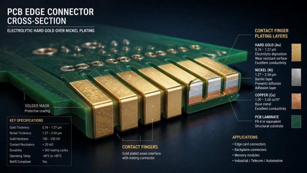
PCB Edge Connector Cross-Section Architecture – Hard Gold Over Nickel Plating
Hard Gold PCB Definition and Electrolytic Plating Mechanics
Hard gold PCB refers to printed circuit boards with an electrodeposited gold-cobalt or gold-nickel alloy layer, typically ranging from 0.25 µm to 5.0 µm (10–200 µin) in thickness, over an electrolytic nickel underlayer. Unlike immersion finishes, hard gold requires an active electrical current and a dedicated plating bus connected to the contact pads. The cobalt or nickel alloying agent—usually 0.1–0.3% by weight—raises the deposit hardness to 130–200 HK (Knoop), which is nearly triple the hardness of pure soft gold used in wire bonding.
For procurement teams, the critical takeaway is that hard gold is not a surface finish you specify by default. It is a functional coating engineered for mechanical wear, not solderability. If your design includes edge connectors, gold fingers, keypad contacts, or press-fit interfaces that must survive 1,000+ mating cycles, hard gold is mandatory. If your design is dominated by SMT pads and BGA footprints, ENIG is the correct choice—and mixing the two on the same board is increasingly common.
Gold Finger PCB Applications and Insertion Cycle Requirements
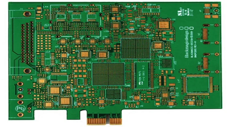
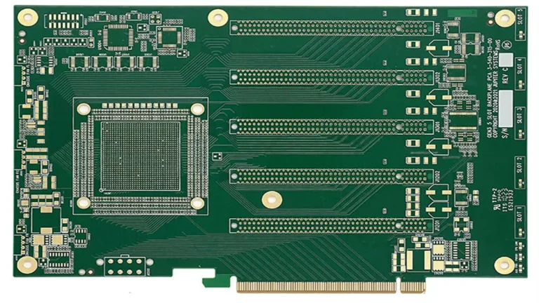
The most visible hard gold application is the gold finger PCB—the edge connector array on memory modules, graphics cards, and server backplanes. PCI-SIG mechanical specifications for PCIe Gen4 and Gen5 add-in cards call for a minimum of 0.8 µm (31 µin) hard gold over 3.8 µm nickel, though procurement professionals increasingly specify 30–50 µin to account for connector vendor tolerance stack-up.
Other high-volume applications include industrial automation backplanes, automotive ECU headers, and telecom line cards. In each case, the procurement specification must tie gold thickness directly to the expected insertion cycle count: 15 µin may suffice for a low-cycle test fixture, while 50 µin is the conservative standard for a 10-year server lifecycle.
Hard Gold vs ENIG: Surface Finish Selection Criteria for Procurement Teams
Durability, Solderability, and Cost Structure Comparison
The hard gold vs ENIG decision is the most consequential surface finish choice in PCB procurement, and conflating the two drives expensive redesigns. ENIG (Electroless Nickel Immersion Gold) deposits a thin pure gold layer—0.05–0.125 µm—over electroless nickel. It delivers exceptional solderability and flatness for fine-pitch QFN and BGA devices, but its hardness sits below 90 HK, making it unsuitable for any mechanical sliding contact.
Hard gold, conversely, cannot be reliably soldered. When gold dissolves into molten solder beyond ~3% by weight, it forms AuSn₄ intermetallics that embrittle joints—a risk that intensifies under lead-free reflow profiles peaking at 245–260°C. The relative cost gap is also significant: ENIG adds roughly 5–15% to bare board cost, while hard gold PCB cost can add 20–50% or more depending on plated area and thickness.
Hybrid Finish Strategy: When to Specify Selective Hard Gold PCB with ENIG
The smartest procurement strategy is often a selective hard gold PCB configuration: ENIG on SMT lands for solderability, hard gold only on edge fingers for wear resistance. This hybrid approach eliminates the need for secondary solder mask steps, reduces gold consumption, and prevents the gold embrittlement risk that occurs when hard gold accidentally covers pads destined for reflow. At Shenzhen Hongda Circuit Technology Co., Ltd., we manufacture both finishes under one roof, allowing hybrid configurations without cross-factory logistics or quality hand-off risks.
Inside Modern Electrolytic Hard Gold Plating: Process Control and Advanced Equipment

Automated VCP Gold Plating Line with Real-Time Bath Analytics
Nickel Underlayer Engineering and Diffusion Barrier Science
Every reliable hard gold deposit begins with the nickel underlayer—not as an afterthought, but as the structural foundation. A sulfamate nickel strike, typically 2.5–5.0 µm thick, serves two functions: it prevents copper diffusion into the gold (which would degrade contact resistance), and it provides a hard substrate that prevents the gold layer from deforming under connector pressure.
At Shenzhen Hongda Circuit Technology Co., Ltd., our dedicated hard gold manufacturing infrastructure includes automated vertical continuous plating (VCP) lines equipped with pulse-reverse rectifiers. These systems deliver sub-micron thickness uniformity across panel formats up to 610 mm × 610 mm, with real-time bath chemistry monitoring that maintains cobalt content within the 0.1–0.3% window required for hardness consistency.
AI-Driven SPC and Real-Time Bath Analytics in Hard Gold PCB Manufacturing
The difference between 1990s-era plating and 2026 manufacturing is the shift from periodic lab sampling to AI-driven SPC process control. Our plating lines integrate inline XRF gauges, closed-loop chemical dosing, and machine-learning algorithms that analyze multivariate process data—current density, bath temperature, agitation flow, and pH—in real time. When the algorithm detects a drift pattern that precedes an out-of-spec deposit, it triggers corrective action before a single panel is compromised.
This predictive capability is not marketing language. Manufacturers deploying AI-enhanced SPC across plating operations have documented defect reductions exceeding 37% and throughput improvements of 22% within six months.
For procurement directors, this translates to fewer incoming QC rejections, more predictable lead times, and a supplier capable of supporting IPC Class 3 programs without manual inspection bottlenecks.
Selective Plating, Blue Glue Masking, and Laser-Aligned Masking Technology
For boards requiring selective hard gold PCB finishes, we employ laser-aligned peelable masking (commonly called “blue glue” in the industry) combined with automated screen-printing registration. This ensures plating boundaries align within ±0.05 mm of the design intent, preventing “gold bleed”—the unnecessary plating of adjacent traces that can inflate material cost by 15–20%.
After plating, the mask is removed cleanly without ionic residue, and panels pass through ultrasonic deionized rinses before final inspection.
Evaluating a China Hard Gold PCB Supplier: Factory Audit Framework for Procurement Directors
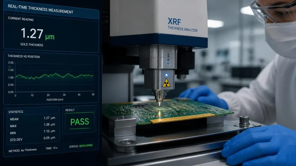
Non-destructive XRF thickness verification measuring micro-inch gold layer uniformity on PCB edge connectors.
In-House Electroplating Lines vs. Outsourcing Risk Assessment
The first question any procurement director should ask during a factory audit is: “Do you own the plating line, or do you subcontract it?” Outsourced hard gold plating introduces three uncontrollable risks: chemistry batch variation, transportation damage between facilities, and broken traceability when defects arise. A qualified china hard gold pcb supplier maintains dedicated in-house electrolytic lines with documented bath analysis logs, daily cobalt content verification, and nickel bath pH control between 3.8–4.2.
At Hongda Circuit, our $12 million investment in dedicated hard gold infrastructure means no third-party plating. Procurement teams auditing our floor can witness live bath analysis, review 5-year test coupon archives, and verify that every lot is traceable to a specific plating line, rectifier settings, and operator shift.
XRF Thickness Verification and Cross-Sectioning Certification Reports
Thickness verification is where commodity suppliers fail and world-class suppliers separate themselves. Demand XRF certification reports showing both gold and nickel thickness at multiple points across the panel—edge, center, and high-current-density corners. Uniformity should be ±10% edge-to-edge. For critical lots, request microsection (cross-sectioning) photos showing columnar nickel morphology and gold grain structure.
Our facility uses 50 µm micro-focus XRF stations calibrated to IPC-4552B guard-band tolerances. This means when your fabrication notes specify “30 µin,” the measurement on our floor carries the same statistical meaning as the measurement in your incoming inspection lab.
IPC Class 2/3 Compliance, ISO 9001, and RoHS Lead-Free Assembly Standards
For U.S. market entry, your hard gold pcb manufacturer must demonstrate compliance with IPC-6012 Class 2 (commercial) or Class 3 (high-reliability) standards, maintain an active ISO 9001:2015 quality management system, and support RoHS lead-free assembly without gold embrittlement failures. Do not accept certificate screenshots at face value—verify the certification scope explicitly includes “electrolytic nickel-gold plating for printed circuit boards” and check the expiration dates. A supplier with ISO 9001 but no IPC Class 3 process controls is not qualified for aerospace or medical programs, regardless of what the sales deck claims.
Hard Gold PCB Cost Factors, Lead Time, and Commercial Volume RFQ Strategy
Gold Market Price Index, Plating Area Calculation, and Thickness Optimization
Hard gold PCB cost is driven by three variables that procurement can influence at the design stage: gold thickness, plated area, and the LBMA spot price. In 2026, sustainability pressures and supply chain constraints continue to elevate precious metal costs, making design-stage optimization more powerful than unit-price negotiation.
Three levers exist:
- Reduce thickness where cycles allow: Dropping from 50 µin to 30 µin for a 500-cycle application cuts gold mass by 40% proportionally.
- Minimize selective area: Review Gerber files for gold bleed around contact pads. A 15% area reduction directly reduces material cost.
- Hybrid finish strategy: Specifying ENIG on SMT lands and hard gold only on fingers eliminates unnecessary gold consumption and secondary masking complexity.
Low MOQ Prototyping, Fast Turnaround, and Bulk Order Logistics for U.S. Buyers
Procurement teams often assume hard gold prototyping requires massive MOQs. That is a legacy constraint. Modern hard gold pcb supplier operations like ours support prototype runs as low as 5 pieces with 24–48 hour engineering review turnaround, allowing validation of contact resistance, insertion force, and chamfer geometry before committing to 1,000+ unit volumes. For bulk orders, panelization efficiency and automated beveling (30° ±1° CNC chamfer) become the cost and quality drivers.
FCA vs DAP Shipping Terms and Supply Chain Risk Mitigation
For U.S.-based procurement directors, shipping terms matter as much as unit price. FCA (Free Carrier) at our Shenzhen facility shifts risk at the handover point, while DAP (Delivered at Place) to your U.S. warehouse consolidates freight and customs complexity under our control. For high-value gold-plated panels, DAP is often preferable because it eliminates buyer-side customs handling that can delay critical production schedules. We recommend DAP for initial bulk orders until your team establishes a freight forwarder relationship.
RFQ Checklist: Key Parameters to Specify in Gerber and Fabrication Notes
Ambiguity in hard gold specifications is the single most expensive mistake in PCB procurement. When requesting quotes, include these parameters explicitly:
| Parameter | Specification Example | Why It Matters |
|---|---|---|
| Gold thickness | 30 µin (0.76 µm) minimum over 3.8 µm nickel | Drives wear life and unit cost directly |
| Plating area | Gold fingers only, rows 1–4, edge connector side | Prevents gold bleed onto SMT pads |
| Hardness requirement | 130–200 HK Knoop | Ensures mechanical durability |
| Bevel angle | 30° ±1° chamfer on connector edge | Prevents insertion damage and snagging |
| Contact resistance | <20 mΩ per IPC-TM-650 | Validates electrical performance |
| Finish hybrid | ENIG on all SMT pads; hard gold on fingers only | Eliminates solderability conflicts |
| Testing protocol | XRF per panel, microsection on 1 coupon per lot | Provides objective quality evidence |
| Compliance class | IPC-6012 Class 3 + RoHS 2.0 | Defines reliability and environmental standard |
Never allow a supplier to “interpret” your gold requirements. A specification of “gold plating” without thickness, hardness, and scope will result in either over-engineering (wasted cost) or under-engineering (field failure).
Ready to Source Hard Gold PCBs with Predictable Quality and Transparent Pricing?
Shenzhen Hongda Circuit Technology Co., Ltd. has built its reputation on the precision that hard gold demands. Our dedicated electrolytic plating lines, AI-driven SPC process control, in-house XRF and cross-sectioning laboratories, and IPC Class 3 certified workflows give procurement directors the audit transparency and lot-to-lot consistency that high-reliability programs require.
Whether you need 5 prototype pieces for insertion-cycle validation or 10,000 units for a server backplane rollout, we support low-MOQ sampling, 24-hour engineering review, and DAP delivery to U.S. facilities. Upload your Gerber files and fabrication notes to www.pcbkr.com or contact our engineering team directly at sales@pcbkr.com for a detailed RFQ response with XRF verification protocol and lead-time options.
FAQ: Hard Gold PCB Procurement—What Buyers Ask Before Signing a PO
How do I verify that a China hard gold PCB supplier actually owns its plating line rather than outsourcing it?
Request a live video walkthrough of the plating floor, ask to see bath analysis logs with today’s date, and demand traceability documentation linking your lot number to a specific rectifier and shift. If the supplier hesitates or routes you to a “partner factory,” you are dealing with a broker or an outsourced process—both of which break quality continuity.
What is the realistic cost difference between hard gold and ENIG for a standard 4-layer board in 2026?
ENIG typically adds 5–15% to bare board cost, while selective hard gold on edge connectors adds 20–50% depending on gold thickness and plated area. For a hybrid finish (ENIG + selective hard gold), expect a 25–35% total premium. The key is that hard gold is never a cost-saving alternative to ENIG; it is a reliability investment for mechanical contact surfaces.
Can I order prototype hard gold PCBs with low minimum quantities and fast turnaround?
Yes. Modern hard gold PCB manufacturers support prototype MOQs as low as 5 pieces with 24–48 hour engineering review. The setup cost for hard gold is higher than HASL or OSP due to masking and bus line preparation, but it is manageable for validation runs. Always prototype before committing to bulk if your design includes new connector geometries or unproven insertion force requirements.
What IPC and RoHS compliance standards should I demand for hard gold PCBs destined for the U.S. market?
Minimum: IPC-6012 Class 2 for commercial electronics, IPC-6012 Class 3 for automotive, medical, or aerospace, plus active ISO 9001:2015 certification. RoHS 2.0 (2011/65/EU) compliance is mandatory for lead-free assembly compatibility. For defense applications, add MIL-G-45204 gold plating requirements and full material traceability.
How do I prevent gold embrittlement when my assembly process uses lead-free solder?
The only reliable prevention is strict selective plating—never allow hard gold on SMT pads that will see reflow. Specify ENIG or OSP on all solderable surfaces, and restrict hard gold to edge connectors, test points, and press-fit interfaces. If rework on a hard gold pad is unavoidable, mechanically remove the gold layer before hand-soldering to prevent AuSn₄ intermetallic formation.
About Author
David Chen https://www.linkedin.com/in/pcbcoming
David Chen boasts an extensive professional background in PCBA manufacturing, PCBA testing, and PCBA optimization, with specialized expertise in high-precision PCBA fault analysis and rigorous PCBA reliability testing. The author has worked with high-layer-count server PCB fabrication, ultra-low-loss backplane stackups, and thermo-mechanical reliability optimization for AI infrastructure projects involving 112G and 224G PAM4 architectures. Skilled in complex circuit design and cutting-edge advanced PCB manufacturing processes, he delivers solutions that elevate product durability and performance across industrial applications. His technical articles focusing on PCBA manufacturing workflows and testing methodologies are widely cited by industry peers, research institutions, and technical platforms, solidifying his reputation as a recognized technical authority in the global circuit board manufacturing sector.