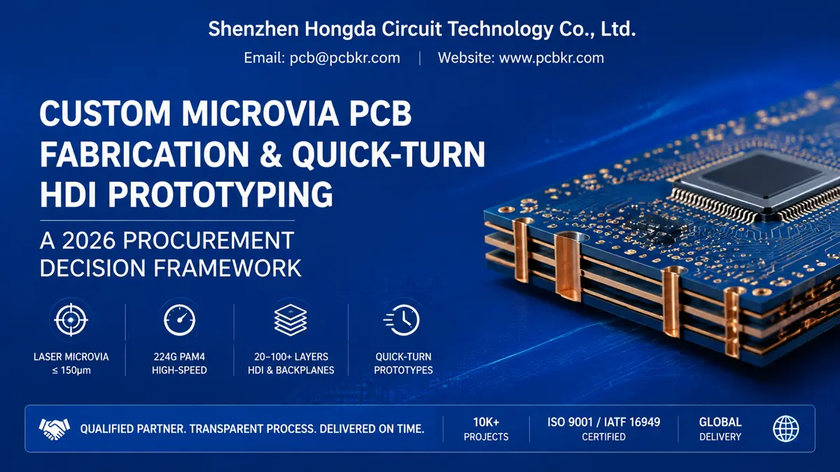
Custom Microvia PCB Fabrication & Quick-Turn HDI Prototyping: A 2026 Procurement Decision Framework
If you are a procurement engineer, supply chain manager, or hardware program director sourcing custom HDI PCB manufacturers in 2026, our full overseas buying manual is Sourcing High-Reliability Microvia PCBs from China: Supply Chain Guide for Global Procurement Teams.
This is not a temporary shortage. The convergence of AI server clusters, 1.6T optical modules, and automotive ADAS electrification has created structural demand for advanced interconnects that traditional subtractive etching cannot deliver. A single NVIDIA Rubin-architecture GPU carrier requires up to seven times the PCB content of a conventional enterprise server, all dedicated design rules are available in Microvia PCBs for AI Servers and HPC Infrastructure: Advanced HDI Manufacturing & Any-Layer Design Guidelines.
The purpose of this guide is straightforward: to provide a procurement decision framework that moves beyond marketing brochures and evaluates microvia PCB suppliers on technical capability, process transparency, and total cost of ownership. Whether you need a quick turn microvia PCB prototype for a 48-hour design iteration or a qualified production partner for 10,000-unit AI server ramps, the following sections reflect actual 2026 manufacturing data, equipment specifications, and quality systems from our facility at Shenzhen Hongda Circuit Technology—not aspirational claims.
2026 Microvia PCB Fabrication Landscape: What Procurement Teams Must Know
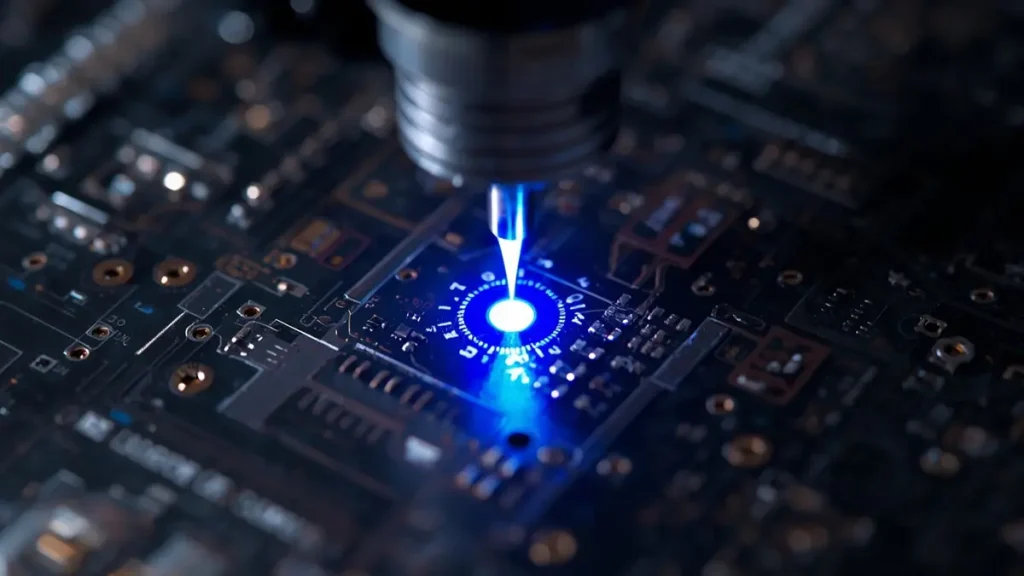
High-Precision UV Laser Drilling in Microvia PCB Fabrication
From 112G to 224G PAM4: Why Microvia Technology Is No Longer Optional
The transition from 112G to 224G PAM4 signaling in advanced High-Density Interconnect (HDI) Microvia PCB Manufacturing | mSAP & SAP Capabilities for AI Server and HPC Applications has fundamentally changed the physics of PCB interconnects. At a 56 GHz Nyquist frequency, a through-hole via stub of just 0.5 mm creates a resonant null at approximately 20 GHz—catastrophically consuming the insertion loss budget before the signal reaches the receiver. For procurement teams qualifying AI server PCB suppliers, this means traditional mechanical drilling and standard FR-4 stackups are no longer viable for high-speed channels.
Microvia PCB technology addresses this through three mechanisms that directly impact procurement specifications:
- Stub length reduction: A laser-drilled blind microvia connecting L1→L2 in a 1.6 mm board presents a stub of approximately 100 μm versus 800 μm for a through-hole. This shifts resonant frequencies above 100 GHz, well beyond current signaling bandwidths.
- Parasitic capacitance control: Microvia pads can be reduced to 200 μm diameter, cutting pad capacitance by 60–70% compared to 400 μm mechanical via pads. This directly improves impedance continuity and reduces differential skew.
- Via-in-pad (VIP) integration: Placing the microvia directly under the BGA pad eliminates dog-bone escape routing, freeing up to two additional signal layers on 0.35 mm pitch devices.
At Hongda Circuit, our 224G PAM4 PCB manufacturing process—in continuous production since Q1 2025—includes depth-controlled back-drilling with ±25 μm stub tolerance, ULP-RTF copper qualification, VIPPO (Via-in-Pad Plated Over) fill inspection, and 4-port VNA S-parameter validation to 70 GHz. First-article deliveries include full impedance coupon reports and insertion-loss/return-loss documentation mapped to IEEE 802.3df templates.
M9-Grade Laminates and the Material Inflection Point
2026 marks the first year of large-scale mass production for M9-grade copper-clad laminates, driven by the NVIDIA Rubin/VR300 platform and 1.6T switch silicon. These materials feature dielectric loss (Df) ≤ 0.0005–0.0008 at 10 GHz and Dk of 2.8–3.0, reducing signal loss by 40% compared to M8-grade predecessors. For procurement teams, this creates a material qualification burden: not every custom HDI PCB manufacturer maintains M9 inventory or has validated lamination cycles for hydrocarbon/modified PPO resin systems.
Our facility maintains strategic partnerships with Panasonic (Megtron 7/8/9), Isola (I-Tera MT40, Tachyon 100G), and domestic M9-qualified suppliers. Each laminate lot undergoes incoming inspection for Dk/Df at 10 GHz, Tg by DSC, and CTE by TMA before release to production. For cost-sensitive programs, we recommend hybrid stackup designs—routing 224G channels on M9 layers while using high-Tg FR-4 for power and ground planes—reducing laminate BOM cost by 38–42% with less than 0.5 dB measured insertion loss penalty.
Custom HDI PCB Manufacturer Evaluation: The Technical Capability Matrix
Laser Drilling Precision and Microvia Aspect Ratio Thresholds
A microvia is defined by IPC-6012 as a blind or buried interconnect with maximum diameter of 150 μm. In 2026 production, leading microvia PCB fabrication facilities routinely produce 50–100 μm holes, with advanced femtosecond systems achieving 20–30 μm at aspect ratios exceeding 15:1. However, procurement teams should distinguish between advertised capability and qualified production yield.
When evaluating a custom microvia PCB manufacturer, demand specifics on:
- Positional accuracy: ±5 μm or better is required for 0.35 mm pitch BGA landing pads. Our Mitsubishi UV/CO₂ laser drilling systems are paired with automated optical registration and real-time beam profiling.
- Aspect ratio limits: For copper-filled blind vias, 15:1 is the practical minimum for AI server applications. Our plating line achieves void-free copper fill at 20:1 using proprietary suppressor/accelerator/leveler chemistry.
- Void detection protocol: 100% 3D X-Ray inspection (AXI) with 5% void sensitivity is non-negotiable for stacked microvia configurations. We utilize Nordson DAGE systems with automated pass/fail sorting.
mSAP vs. SAP: Selecting the Right Fine-Line Process for Your Application
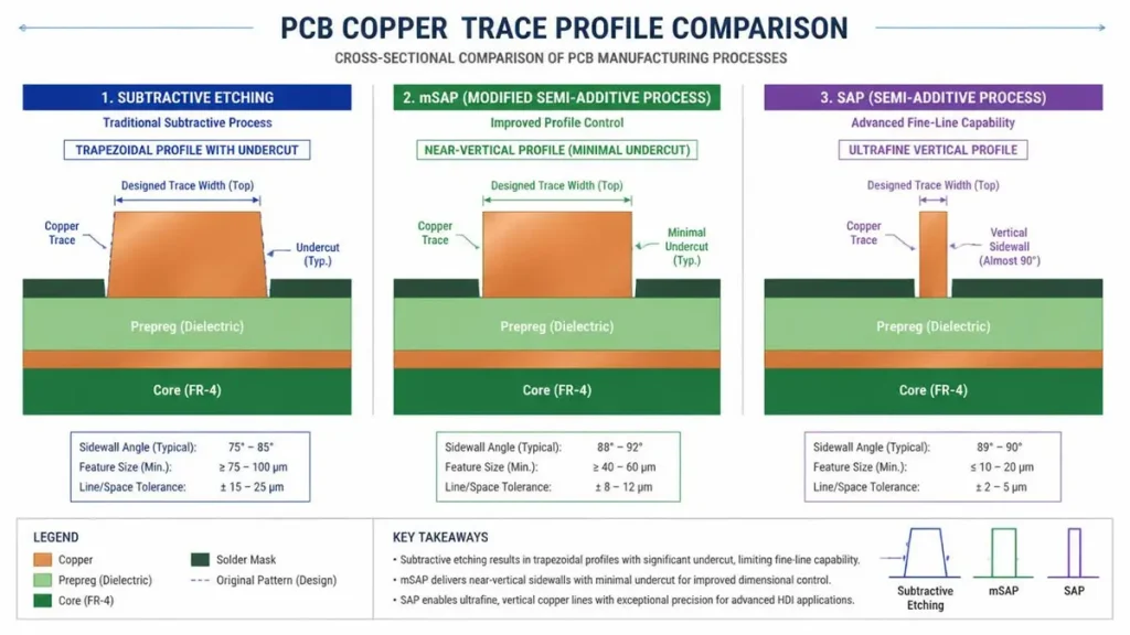
PCB Copper Trace Profile Comparison: Subtractive Etching vs. mSAP vs. SAP
mSAP has become the dominant fabrication method for advanced HDI in 2026, you can get full process details from mSAP Process in Microvia PCB Fabrication: Why Modified Semi-Additive Technology Is the Only Path to Sub-15μm Routing for AI Chip Carriers Understanding the distinction between mSAP and full SAP PCB fabrication is critical for procurement specification:
| Parameter | Subtractive Etching | mSAP | SAP |
|---|---|---|---|
| Starting Copper | 18–35 μm foil | 1.5–3 μm thin foil | <1 μm electroless seed |
| Line/Space (Production) | 50–100 μm | 15–30 μm; 8–10 μm qualified | 5–20 μm |
| Trace Profile | Trapezoidal, undercut | Near-vertical, minimal undercut | Vertical, no undercut |
| Impedance Control | ±10% typical | ±5% typical | ±3% typical |
| Relative Cost | 1.0× baseline | 1.5–2.5× | 3.0–5.0× |
| Best Application | Standard multilayer | Advanced HDI, AI server, SLP | IC substrate, interposer, RDL |
Procurement recommendation: For AI server GPU carriers, switch fabrics, and high-density motherboards, specify mSAP as the baseline in High-Density Interconnect (HDI) Microvia PCB Manufacturing. Only mandate SAP if your design requires sub-15 μm routing for chiplet integration or CoWoS-style advanced packaging. At Hongda Circuit, our mSAP line operates with SCREEN Ledia LDI exposure (±1.5 μm registration) and a 3-in-1 horizontal plating line that improves throughput by 40% while reducing chemical consumption. We routinely produce 20 μm/20 μm line/space in volume and have qualified 8 μm/8 μm for substrate-like PCB (SLP) builds.
Copper-Filled Microvia and VIPPO Reliability Standards
Stacked microvia PCBs—where four or more blind vias align vertically—represent the highest-risk, highest-reward configuration in HDI procurement. The cumulative thermal expansion stress at the via base can exceed the fracture threshold of the copper barrel during thermal cycling. This is why copper-filled microvia technology (VIPPO) is non-negotiable for high-reliability applications.
Our qualification protocol includes:
- Void-free copper fill verified by microsection analysis per IPC-TM-650 2.1.1 on every production lot
- Planarization control to ensure flat landing surfaces for subsequent component attachment
- Thermal shock validation (−65°C to +150°C, 1000 cycles) for AI server PCB qualification
- IST (Interconnect Stress Test) for mission-critical builds, applying accelerated thermal cycling to detect latent defects before shipment
Quick Turn Microvia PCB Prototyping: Accelerating NPI Cycles
48-Hour to 7-Day Turnaround Tiers for HDI Builds
In AI server development, schedule compression is often more valuable than unit cost reduction. A delayed prototype can push a product launch by an entire quarter. Standard industry lead times for quick turn microvia PCB prototypes range from 10–15 working days for 4–8 layer HDI builds and 15–25 days for complex 12+ layer or Any-Layer HDI designs. These timelines are incompatible with modern hardware iteration cycles.
At Hongda Circuit, we have structured our quick-turn HDI PCB prototype service into four velocity tiers:
| Build Complexity | Turnaround | Application |
|---|---|---|
| Standard 4–8 layer HDI | 48 hours | IoT, wearable, sensor validation |
| 10–16 layer mSAP with copper-filled microvias | 5 days | AI edge device, automotive ECU |
| 20+ layer backplane with back-drilling | 7 days | Switch fabric, HPC accelerator |
| 40–104 layer orthogonal backplane | 10–14 days | Hyperscale data center interconnection |
These timelines assume material in stock and DFM clearance. Our AI-driven ERP system optimizes production scheduling based on real-time equipment availability, material readiness, and test capacity, ensuring urgent prototypes are not delayed by lower-priority volume orders.
DFM Engagement Before Cutting Metal
The most expensive PCB is one that cannot be built reliably. Our engineering team provides complimentary pre-production DFM reviews that typically identify 3–5 design optimizations per project, including:
- Stackup optimization: Balancing signal integrity, manufacturability, and material cost
- Microvia placement: Avoiding via-in-pad on SMT pads that will undergo wave soldering
- Trace spacing: Ensuring mSAP line/space targets are achievable with your density requirements
- Impedance target feasibility: Confirming that your stackup and trace geometry can hit ±5% tolerance with available materials
- Test point accessibility: Ensuring 100% electrical test coverage without probe damage to fine-pitch components
We commit to 24-hour DFM feedback for standard HDI builds and 48-hour turnaround for complex multilayer or rigid-flex designs.
Manufacturing Footprint and Supply Chain Resilience
Equipment Portfolio and Metrology Infrastructure
Advanced microvia PCB fabrication requires advanced metrology—you cannot control what you cannot measure. Our 2026 capital equipment investment exceeds $12 million in dedicated fine-line and high-speed manufacturing infrastructure:
| Equipment | Manufacturer/Model | Capability | Application |
|---|---|---|---|
| LDI Exposure | SCREEN Ledia | ±1.5 μm registration, zero-mask patterning | mSAP fine-line imaging, Any-Layer HDI |
| Laser Drilling | Mitsubishi UV/CO₂ | 50–100 μm microvias, ±5 μm positional accuracy | Blind via formation, HDI builds |
| Femtosecond Laser | In-house qualified picosecond/femtosecond source | 20–30 μm microvias, 50 μm rigid-flex vias | Advanced interposer, wearable HDI |
| Lamination | LAUFFER | Temperature/pressure real-time feedback, CTE-matched cycles | High-layer-count backplanes, rigid-flex |
| Plating Line | HX Automated | 3-in-1 desmear + electroless + electrolytic, ±3% uniformity | mSAP copper deposition, via filling |
| X-Ray Inspection | Nordson DAGE | 3D AXI, 5% void detection sensitivity | Microvia fill verification, BGA inspection |
| XRF Analysis | In-house micro-focus XRF | 50 μm spot size, ±8% thickness uniformity | Hard gold, ENIG, immersion tin verification |
| Flying Probe Test | In-house systems | 100% electrical test, 20 μm probe accuracy | Prototype and low-volume validation |
| Impedance Test | In-house TDR systems | ±5% impedance tolerance verification | 224G PAM4, high-speed differential pairs |
Certification Stack for Automotive, Medical, and Aerospace Procurement
For regulated industries, certifications are evidence of documented process control, traceability, and continuous improvement—not checkboxes. Our quality management system is certified to:
- ISO 9001:2015 — Quality Management Systems
- AS9100D — Aerospace Quality Management
- IPC-6012 Class 3/3A — Performance Specifications for Rigid PCBs
- ISO 13485 — Medical Device Quality Management
- IATF 16949 — Automotive Quality Management
- UL Recognition — Flame resistance and electrical safety
When evaluating a custom HDI PCB manufacturer for mission-critical applications, request certificate numbers and verify them directly with the issuing registrar (SGS, TÜV, Bureau Veritas). At Hongda Circuit, we provide certificate copies and welcome third-party audits by customer quality teams. Our Unified Social Credit Code (China Tax ID) is 91440300MA5F6CA091.
Cost Optimization Strategies for Microvia PCB Programs
Layer Count Reduction via Any-Layer HDI and Skip-Via Design
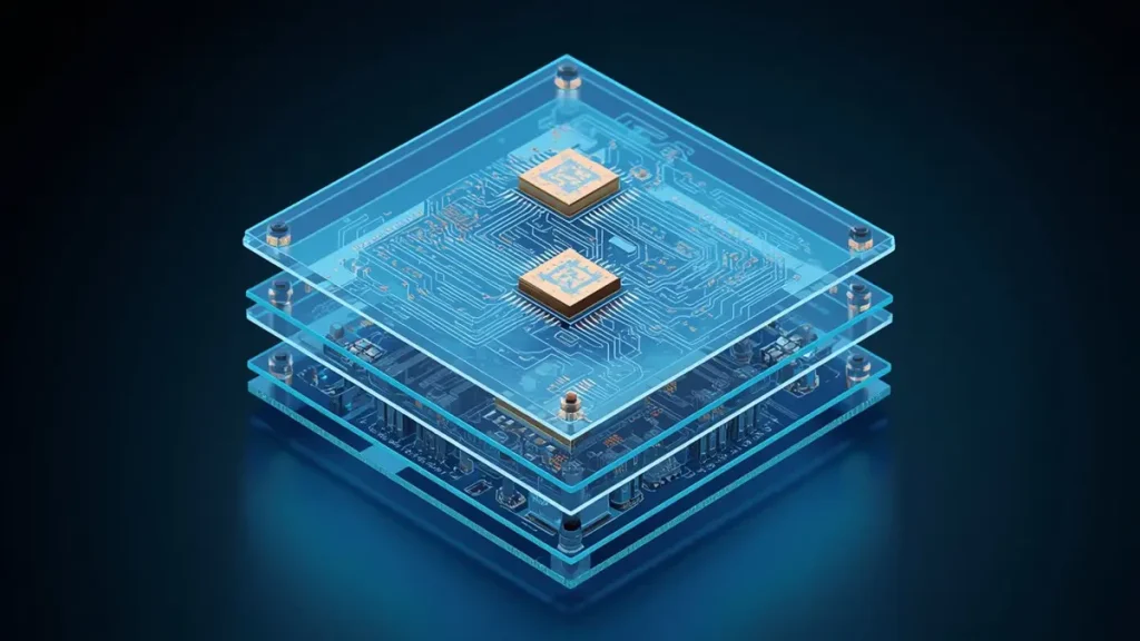
3D Isometric Multi-Layer Any-Layer HDI PCB Stackup Architecture
Microvia PCB cost is driven first and foremost by lamination cycles. Each additional lamination stage adds 15–25% to processing cost. Procurement teams can optimize unit economics without compromising performance by:
- Consolidating microvia sizes to reduce laser setup changes and improve drilling throughput
- Using skip-via or Any-Layer HDI architectures to bypass intermediate layers, reducing total layer count
- Avoiding stacked microvias unless copper filling is explicitly specified—staggered configurations distribute mechanical stress and improve yield
- Specifying standard 0.35 mm BGA pitch instead of 0.25 mm when electrical performance allows, eliminating the need for extreme mSAP or SAP processing
These decisions routinely reduce unit cost by 20–30% on custom microvia PCB fabrication programs without functional compromise.
Material Hybridization for 224G PAM4 Budget Control
M9-grade ultra-low-loss laminates cost 3–5× standard FR-4. For procurement teams under cost pressure, we recommend strategic material placement: use M9 or Megtron 7 only for high-speed signal layers, and specify high-Tg FR-4 or Megtron 6 for power planes and low-speed routing. This hybrid approach, validated across 1,800+ production panels at Hongda Circuit, reduces laminate BOM cost by 38–42% while maintaining full 224G PAM4 channel compliance.
Frequently Asked Questions: Microvia PCB Procurement from a Buyer’s Perspective
What is the difference between mSAP and SAP, and which process should I specify for my AI server PCB?
mSAP (Modified Semi-Additive Process) uses a 1.5–3 μm thin copper foil as the starting layer, images the trace pattern, selectively plates copper to build trace height, and flash-etches the remaining seed layer. It achieves 15–30 μm line/space in production and is the standard for advanced HDI, substrate-like PCBs, and AI server applications.
SAP (Semi-Additive Process) starts with an electroless copper seed layer under 1 μm thick. It enables 5–20 μm line/space but requires substrate-grade cleanroom environments and DUV lithography, making it significantly more expensive and limited to IC substrates and interposers.
Recommendation: For AI server GPU carriers, switch fabrics, and high-density motherboards, specify mSAP as the baseline. Only specify SAP if your design requires sub-15 μm routing for chiplet integration or advanced packaging applications.
How do I verify that a microvia PCB manufacturer can actually produce 224G PAM4-qualified boards?
224G PAM4 PCB manufacturing is not a marketing claim—it is a validated production process. When qualifying a supplier, demand:
S-parameter test reports from actual production boards, showing insertion loss and return loss through 56 GHz
Impedance coupon data with TDR traces demonstrating ±5% tolerance across the panel
Material qualification documentation proving the laminate Dk/Df was measured at 10 GHz (not just datasheet values)
Back-drilling microsections showing remaining stub length <0.2 mm
Thermal reliability data (IST or thermal shock) for the specific via stackup configuration you require
At Hongda Circuit, our 224G PAM4 process has been in continuous produc
tion since Q1 2025, with full test documentation available under NDA for qualified procurement teams.
What drives microvia PCB cost, and how can I optimize my design for manufacturability?
Microvia PCB cost is driven by five primary factors:
Layer count and lamination cycles: Each additional lamination stage adds 15–25% to processing cost. Optimize by using skip-vias or Any-Layer HDI to reduce layer count.
Microvia density and aspect ratio: Higher hole densities require slower laser drilling speeds. Aspect ratios above 12:1 require specialized plating chemistry.
Line/space requirements: mSAP adds 1.5–2.5× cost versus subtractive etching. Do not specify mSAP unless your design genuinely requires <30 μm traces.
Material grade: M8/M9 ultra-low-loss laminates cost 3–5× standard FR-4. Use them only for high-speed signal layers.
Surface finish and special processes: ENEPIG costs more than ENIG; back-drilling adds a machining step.
DFM optimization strategies: Consolidate microvia sizes, avoid stacked microvias unless copper filling is specified, and use standard 0.35 mm BGA pitch instead of 0.25 mm when possible. These decisions can reduce unit cost by 20–30%.
What certifications should I demand from a microvia PCB supplier serving automotive or medical markets?
For automotive microvia PCB procurement, IATF 16949 is mandatory. This certification requires Advanced Product Quality Planning (APQP), Production Part Approval Process (PPAP) submission, full lot traceability, and ppm-level quality reporting.
For medical device PCBs, ISO 13485 is the baseline, with additional requirements for risk management documentation per ISO 14971, biocompatibility assessment for implantable devices, and sterile handling protocols where applicable.
For aerospace and defense, AS9100D adds configuration management, counterfeit parts prevention, and full supply chain traceability. At Hongda Circuit, we hold all three certifications and provide complete documentation packages for customer quality audits.
What is the typical lead time for microvia PCB prototypes, and how does Shenzhen Hongda Circuit Technology support rapid turnaround?
Standard lead times in the industry for quick turn microvia PCB prototypes range from 10–15 working days for 4–8 layer builds, and 15–25 days for complex 12+ layer or Any-Layer HDI designs.
At Shenzhen Hongda Circuit Technology, we offer:
48-hour prototype turnaround for standard 4–8 layer HDI builds (material in stock, no DFM issues)
5-day turnaround for 10–16 layer mSAP builds with copper-filled microvias
7-day turnaround for 20+ layer backplanes with back-drilling
24/7 engineering support with dedicated account managers for enterprise clients
30-minute inquiry response and 1-hour RFQ triage during business hours (UTC+8)
Our AI-driven ERP system optimizes production scheduling based on equipment availability, material readiness, and test capacity, ensuring that urgent prototypes are not delayed by lower-priority volume orders.
Choosing the Right Microvia PCB Partner for 2026 and Beyond
The High-Density Interconnect (HDI) Microvia PCB Manufacturing market in 2026 is defined by a single reality: demand for advanced HDI, mSAP, and high-layer-count backplanes has outstripped capable manufacturing capacity. AI data center expansion, 5G-Advanced deployment, and automotive electrification are consuming premium PCB capacity faster than new facilities can be qualified. In this environment, choosing a supplier based on unit price alone is a high-risk strategy.
The procurement teams that will succeed are those that evaluate suppliers on total cost of ownership: technical capability, quality system maturity, DFM engagement depth, and supply chain resilience. A microvia PCB that fails in thermal cycling after six months in an AI server rack costs far more than a 20% premium on unit price would have saved.
At Shenzhen Hongda Circuit Technology Co., Ltd., we have built our business on the premise that transparency builds trust. Our equipment list, capability data, and certification documentation are available for verification. Our engineering team provides proactive DFM consultation before a single panel is cut. Our quality system is audited, validated, and continuously improved.
Whether you are designing the next generation of AI training clusters, autonomous vehicle compute platforms, or satellite communication payloads, we invite you to evaluate our capabilities against your most demanding requirements.
Ready to discuss your microvia PCB project?
- Email:sales@pcbkr.com
- Engineering:pcb@pcbkr.com
- Phone: +86 0755 23720053
- Website:www.pcbkr.com
- Address: Room 1608-1610, Research Development Comprehensive Building, Baoyunda Logistics Center, Baoan, Shenzhen, China
- Unified Social Credit Code: 91440300MA5F6CA091
Submit your Gerber files and stackup requirements today for a complimentary DFM review and detailed quotation within 30 minutes.
About the Author:
David Chen https://www.linkedin.com/in/pcbcoming
David Chen boasts an extensive professional background in PCBA manufacturing, PCBA testing, and PCBA optimization, with specialized expertise in high-precision PCBA fault analysis and rigorous PCBA reliability testing. The author has worked with high-layer-count server PCB fabrication, ultra-low-loss backplane stackups, and thermo-mechanical reliability optimization for AI infrastructure projects involving 112G and 224G PAM4 architectures. Skilled in complex circuit design and cutting-edge advanced PCB manufacturing processes, he delivers solutions that elevate product durability and performance across industrial applications. His technical articles focusing on PCBA manufacturing workflows and testing methodologies are widely cited by industry peers, research institutions, and technical platforms, solidifying his reputation as a recognized technical authority in the global circuit board manufacturing sector.
© 2026 Shenzhen Hongda Circuit Technology Co., Ltd. All technical data subject to update. Contact engineering for latest specifications.