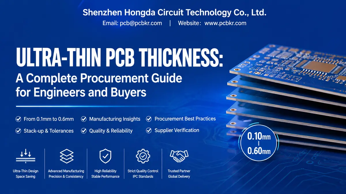
Ultra-Thin PCB Thickness: A Complete Procurement Guide for Engineers and Buyers
When your product team says “we need this board as thin as possible,” that single sentence triggers a chain of decisions that will affect your BOM cost, assembly yield, and field reliability. Refer to our complete ultra‑thin PCB manufacturing guide for a full overview of materials, processes and cost considerations. Most buyers start the conversation with a simple question — how thin can you go? — but the answer that actually matters depends on layer count, copper weight, material type, panel size, and whether your assembly house has ever handled a 0.1 mm substrate before.
At Shenzhen Hongda Circuit Technology Co., Ltd. , we have been manufacturing ultra-thin rigid PCBs down to 0.10 mm finished thickness since 2012. Our factory in Shenzhen runs a dedicated thin-board production line with vacuum lamination, CO₂/UV hybrid laser drilling, and LDI direct imaging — equipment that becomes non-negotiable once you drop below 0.30 mm. This guide walks through the full ultra-thin PCB thickness landscape from a procurement perspective: what the numbers mean, where the manufacturing risks hide, and how to verify that a supplier’s claimed minimum PCB thickness is something they can actually ship in volume, not just build once in a lab.
What Is Ultra-Thin PCB Thickness? Understanding the Basics for Your Next Design
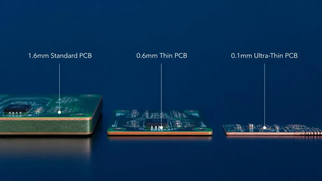
Side-by-Side Thickness Comparison of Standard (1.6mm), Thin (0.6mm), and Ultra-Thin (0.1mm) PCBs
Ultra-Thin PCB Thickness vs. Standard PCB Thickness: Where the Line Gets Drawn
There is no IPC standard that stamps an official “ultra-thin” badge on a specific millimeter value. In practice, the industry sorts PCB thickness into three bands:
- Standard PCB: 1.0 mm to 1.6 mm. This is the default. Most connectors, enclosures, and assembly fixtures assume 1.57 mm (62 mil).
- Thin PCB: 0.6 mm to 0.8 mm. Common in wearables, card-type devices, and modules where height matters but mechanical strength cannot collapse.
- Ultra-thin PCB: roughly 0.1 mm to 0.4 mm. This is where standard FR-4 starts to behave like a piece of stiff paper, and where your supplier’s equipment list becomes more important than your Gerber file.
The confusion starts when one factory calls 0.6 mm “ultra-thin” while another reserves that label for 0.2 mm and below. At Hongda Circuit, we classify 0.1 mm–0.4 mm as our ultra-thin production window, with 0.6 mm handled on our standard thin-board line. If you are comparing quotes, always ask for the finished board thickness — not the marketing label.
Finished Board Thickness vs. Material Thickness: What Buyers Often Get Wrong
A 0.20 mm finished board is not made from a 0.20 mm core. The final PCB thickness stacks up from the core, prepreg, copper foil, solder mask, and surface finish. On a typical 2-layer 0.20 mm board with 1/2 oz copper and ENIG finish, the raw core might only be 0.10 mm. The rest comes from copper plating, dielectric bonding layers, and the 10–25 µm of solder mask on each side.
Buyers who specify “0.2 mm core” instead of “0.2 mm finished” end up with boards that measure 0.28 mm after plating and masking — too thick for the enclosure, too late to fix without a re-spin. Our standard practice at Hongda Circuit is to confirm finished board thickness with a ±0.03 mm tolerance on anything below 0.30 mm, and we provide a detailed stack-up drawing with every first article so you know exactly where each micron sits.
Ultra-Thin PCB Thickness Range: From 0.1mm to 0.6mm, What Each Spec Means for Your Product
0.6mm and Below: Thin PCB Board Thickness for Space-Critical Modules
At 0.6 mm, you are still working with conventional FR-4 and standard drilling. Most SMT lines handle 0.6 mm without custom pallets, and the board has enough stiffness to survive depanelization with a standard router. The trade-off is modest: you save roughly 60% of the thickness compared to 1.6 mm, but warpage during reflow becomes visible if your copper distribution is unbalanced.
This thickness fits IoT gateways, industrial sensor modules, and handheld devices where every millimeter counts but the product still sees moderate mechanical handling. Lead times and pricing stay close to standard boards because the factory does not need to slow down drilling feeds or switch to thin-core lamination cycles.
0.1mm–0.4mm: The Core Ultra-Thin PCB Thickness Window Most Buyers Need
This is where the real engineering starts. Within the 0.1–0.4 mm band, each 0.05 mm step changes what is possible:
| Finished Thickness | Typical Positioning | What It Means for Procurement |
|---|---|---|
| 0.40 mm | Thin / ultra-thin boundary | 4-layer possible with 1/2 oz copper. Good mechanical stability. Most assembly houses handle it without drama. |
| 0.30 mm | Standard ultra-thin | Common for 2-layer rigid boards. 4-layer possible but requires thin-core prepreg (106/1080 style). |
| 0.25 mm | Aggressive ultra-thin | The compromise point between thickness and strength. Laser drilling recommended for vias. |
| 0.20 mm | Practical minimum for rigid | Widely quoted as the minimum PCB thickness for mass-produced rigid boards. 2-layer standard; 4-layer possible with specialized stack-up. |
| 0.15 mm | Extreme ultra-thin | Requires thin-core FR-4 or polyimide. Handling fixtures mandatory. Not every assembly house will touch it. |
| 0.10 mm | Rigid limit | The edge of what FR-4 can do before you switch to flex. Confirmed capability only; always verify with stack-up review. |
At Hongda Circuit, 0.20 mm and 0.30 mm represent roughly 70% of our ultra-thin order volume. These thicknesses hit the sweet spot: thin enough for miniaturized consumer electronics, thick enough that we do not have to reject 15% of the panels for handling damage.
Common Ultra-Thin PCB Thickness Specifications Table
If you are writing a procurement spec and need to lock a number, start with the table above. Do not treat these as universal standards — one supplier’s 0.20 mm minimum might assume 2 layers and 1/3 oz copper, while another might need 0.25 mm for the same stack-up because their drill aspect ratio limits are tighter. Always cross-reference the thickness with layer count, copper weight, and panel size before you freeze the BOM.
Minimum PCB Thickness: How Thin Can a PCB Be in Real Production?

Precision laser drilling system creating microvias on ultra-thin PCB substrates
What Is the Minimum PCB Thickness for Rigid Boards? (The 0.1mm–0.2mm Reality)
The honest answer to “how thin can a PCB be?” is: it depends on who you ask and how many units you need.
In volume production, 0.20 mm is the minimum PCB thickness that most qualified rigid PCB manufacturers can deliver with a Cpk above 1.33. A handful of factories — Hongda Circuit included — run production lots at 0.10 mm–0.15 mm, but that capability sits on a narrow foundation: thin-core FR-4 or polyimide substrates, 1/3 oz copper, single or double-sided builds, and panel sizes typically under 100 mm × 100 mm to keep warpage manageable.
The 0.10 mm figure you sometimes see quoted is almost always a material thickness (the dielectric core alone), not the finished board. Once you add copper, plating, mask, and finish, a “0.10 mm core” becomes 0.14–0.16 mm finished. If your mechanical drawing has a hard 0.10 mm ceiling, you need to have that conversation before the first panel goes into the etcher.
Factors That Push Minimum PCB Thickness Higher Than You Expect
Buyers often receive a quote for 0.20 mm, submit a 4-layer Gerber with 1 oz copper and 0.3 mm via holes, and get a DFM rejection. Here is why the minimum PCB thickness on a datasheet rarely applies to your specific design:
- Layer count: Each additional pair of layers needs prepreg and core. A 4-layer 0.20 mm board needs two cores at roughly 0.06 mm each plus two prepreg sheets — already a tight squeeze. At 6 layers, 0.20 mm is practically impossible with standard materials.
- Copper weight: 1 oz copper is 35 µm per side. On a 0.20 mm board, the copper alone accounts for 35% of the total thickness. Drop to 1/3 oz (12 µm) and you buy yourself more dielectric room.
- Via diameter and density: Small vias in thin boards create high aspect ratios. A 0.15 mm via in a 0.20 mm board is a 1.33:1 ratio — manageable. The same via in a 0.10 mm board is 0.67:1, which is actually easier to plate, but the surrounding material is so fragile that drill breakthrough cracks the panel.
- Panel size: A 0.20 mm board measuring 50 mm × 50 mm behaves very differently from one measuring 200 mm × 150 mm. Larger panels warp more, require more support during conveyor transport, and see higher scrap rates.
- Surface finish: HASL subjects the board to thermal shock (265–270 °C molten solder). At 0.20 mm and below, that thermal gradient can curl the panel permanently. ENIG, OSP, or immersion silver are safer choices but add cost.
- Assembly requirement: If your CM plans to run the board through a standard reflow oven on a steel pallet, 0.20 mm might survive. If they expect to hand-solder connectors afterward, the localized heat will delaminate thin FR-4.
At Hongda Circuit, our DFM team reviews every ultra-thin inquiry against these six factors before we confirm a thickness. We have seen too many projects where the designer chose 0.15 mm for space reasons, only to discover that the BGA package they selected needs a 0.25 mm substrate to survive reflow.
Below 0.1mm: When Flexible PCB Becomes the Only Viable Path
Once you need finished thickness below 0.10 mm, rigid FR-4 exits the conversation. Flexible circuits built on polyimide (PI) film can achieve dielectric layers down to 25 µm (0.025 mm) with 12 µm copper, yielding a finished flex circuit around 50–75 µm depending on coverlay and stiffener choices. That is not a “thinner rigid board” — it is a different technology with different design rules, different assembly methods, and different cost structures.
If your project is hovering at the 0.08–0.10 mm boundary, we will typically recommend a rigid-flex hybrid or a polyimide-based ultra-thin rigid board rather than pushing FR-4 past its mechanical limit. The PI substrate costs more per square meter, but the yield improvement usually pays for the material upgrade.
What Is the Thinnest PCB? Separating Lab Curiosity from Mass-Production Reality
Thinnest Rigid PCB: Why 0.2mm Is the Practical Sweet Spot
Research labs and university groups have demonstrated rigid PCBs down to 0.05 mm using exotic substrates and micro-transfer printing. Those boards make interesting conference papers. They do not make interesting purchase orders.
For procurement teams, the thinnest PCB that matters is the thinnest one your supplier can build repeatably in lot sizes of 1,000+ units with a first-pass yield above 90%. In our experience at Hongda Circuit — backed by 12 years of production data — that number is 0.20 mm for 2-layer rigid FR-4, and 0.30 mm for 4-layer builds. We have shipped 0.10 mm and 0.15 mm lots for medical sensor and security card applications, but those runs demand:
- Dedicated thin-board tooling slots on the panel frame
- Vacuum hold-down during every conveyor process
- Custom test fixtures that support the panel without flexing it
- Hand-sorting instead of automated depanelization
Those constraints add 20–40% to the unit cost and extend lead time by 3–5 days. If your product roadmap needs 50,000 units per month at 0.10 mm, you need a supplier who has invested in a full thin-board production cell, not just a pilot line.
Thinnest Flexible PCB: How 25μm Substrates Change the Thickness Conversation
Flexible PCB technology operates in a different thickness universe. A single-sided flex circuit on 25 µm polyimide with 12 µm copper and 25 µm coverlay finishes around 65 µm — roughly 40% of the thinnest rigid FR-4 board we produce. Double-sided flex with plated through-holes typically runs 0.10–0.15 mm finished.
Buyers sometimes ask us to “make the rigid section as thin as flex.” That is a category error. Rigid boards need glass reinforcement for dimensional stability during drilling and plating. Remove the glass (as flex does) and you lose the rigidity that makes automated assembly possible. If your design needs both ultra-low thickness and some rigidity, a rigid-flex board with a 0.10 mm flex section and 0.20 mm rigid stiffener is usually the better procurement choice.
Theoretical Thinnest PCB vs. Practical Minimum PCB Thickness for Procurement
Here is the distinction that saves procurement teams from mid-project supplier switches:
- Theoretical thinnest PCB: What a process engineer can build once, under ideal conditions, with no concern for cycle time or yield.
- Practical minimum PCB thickness: What the factory can build every day, with standard operators, on equipment that is already booked for other orders, while hitting your target Cpk and delivery date.
When a supplier quotes 0.10 mm, ask which category that number belongs to. At Hongda Circuit, we quote two thicknesses on every ultra-thin RFQ: the “capability limit” (what our equipment can physically do) and the “production recommendation” (what we advise for your volume and reliability targets). Those numbers are rarely the same, and the gap between them is where most procurement risks live.
Ultra-Thin FR4 PCB and Material Choices: What Determines How Thin You Can Go
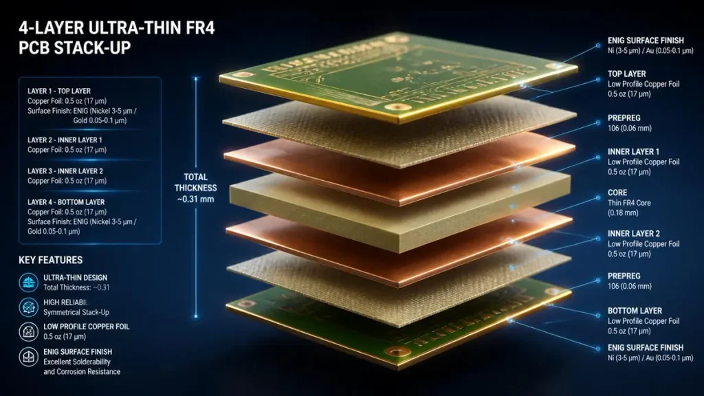
Detailed 4-layer ultra-thin FR4 PCB stack-up design (~0.31mm total thickness) featuring 106 prepreg and low-profile copper foil
Ultra-Thin FR4 PCB: Can Standard Material Really Hit 0.15mm?
Yes — with caveats. Standard FR-4 (IPC-4101/21) is available in core thicknesses down to 0.05 mm from material vendors like NanYa, ITEQ, and Kingboard. The problem is not the raw material; it is what happens to that material when it goes through drilling, plating, etching, and thermal cycling.
At Hongda Circuit, our ultra‑thin FR‑4 line uses high‑Tg, non‑halogen thin‑core laminates (Tg ≥ 170 °C) because standard Tg material (130–140 °C) becomes rubbery during lead‑free reflow and loses dimensional stability. For deeper guidance on substrate selection and core‑driven stack‑up rules, read our ultra‑thin core PCB procurement guide.
Our typical ultra-thin FR-4 stack-ups include:
- 0.15 mm finished, 2-layer: 0.10 mm core + 1/3 oz base copper + plating + ENIG
- 0.20 mm finished, 2-layer: 0.15 mm core + 1/2 oz copper + plating + ENIG
- 0.30 mm finished, 4-layer: Two 0.06 mm cores + 106 prepreg + 1/2 oz outer, 1/3 oz inner
These are production-proven recipes, not theoretical stack-ups. We maintain them as standard build codes so repeat orders do not require re-qualification.
Polyimide and BT Resin: When Thinner Than 0.3mm Becomes Non-Negotiable
Polyimide (PI) and BT (Bismaleimide Triazine) resins enter the conversation when you need three things simultaneously: thickness below 0.30 mm, higher thermal resistance than standard FR-4, and better dimensional stability during temperature cycling.
- Polyimide: Best for applications that need some bend capability or extreme thinness. PI core down to 0.025 mm is commercially available. The trade-off is moisture absorption — PI picks up water faster than FR-4, so bake-out before assembly is mandatory.
- BT resin: Common in IC substrate and memory module applications. BT offers Tg above 180 °C, low CTE, and excellent adhesion to thin copper. We use BT for 0.10 mm–0.20 mm builds where the board will see repeated thermal shock (automotive sensors, power modules).
Material selection is not a “pick the thinnest” exercise. At Hongda Circuit, our material engineers review the end-use environment — operating temperature, humidity, mechanical load, and assembly thermal profile — before recommending a substrate. A 0.20 mm board that delaminates in the field because the material was chosen for thinness rather than thermal performance is a procurement failure, not a design failure.
Thin PCB Design Trade-offs: What Every Buyer Should Know Before Committing to a Thickness
The Real Benefits of Thinner PCBs (Beyond Just Saving Space)
Space and weight are the obvious wins. A 0.20 mm board weighs roughly 40% less than a 1.6 mm equivalent, and in a wearable deSpace and weight are the obvious wins. A 0.20 mm board weighs roughly 40% less than a 1.6 mm equivalent, and in a wearable device with a 30 mm × 30 mm PCB, that difference is measurable in grams. Review our full guidance on ultra‑thin PCB design to mitigate mechanical and signal‑integrity risks when selecting your target board thickness. vice with a 30 mm × 30 mm PCB, that difference is measurable in grams. But there are secondary benefits that affect procurement decisions:
- Shorter via stubs: In multilayer boards, thinner dielectrics mean shorter through-hole stubs, which improves signal integrity for high-speed interfaces. If your design runs USB 3.0 or MIPI lanes, dropping from 1.2 mm to 0.60 mm can reduce stub resonance without backdrilling.
- Improved thermal path to housing: Thin boards sit closer to the product enclosure. With a thermal interface pad, heat from the component side transfers to the housing faster than it would through 1.6 mm of FR-4.
- Reduced material cost per panel: Less material = lower laminate cost. On high-volume orders, the material savings can offset the handling premium.
The Hidden Costs and Risks of Pushing for the Thinnest PCB Possible
The risks show up in places buyers do not always anticipate:
Mechanical fragility: A 0.15 mm board can crack if an operator picks it up by one corner. We have seen assembly houses reject entire lots because their pick-and-place machine’s conveyor belts flexed the panels during loading. The fix — custom carrier pallets — adds setup cost and extends lead time.
Warpage: Thin boards warp more, especially when copper distribution is asymmetric. A board with a solid ground plane on layer 1 and sparse traces on layer 2 will curl like a potato chip after reflow. The design fix (copper balancing) takes time. The procurement fix (accepting a wider flatness tolerance) affects connector fit.
Testing complexity: Flying probe testers apply downward force on each probe. On a 0.20 mm board, that force flexes the substrate, causing false opens. We use vacuum hold-down fixtures for all ultra-thin flying probe tests, which adds 2–3 hours to the test cycle.
Assembly premium: Most contract manufacturers charge 15–40% more for boards below 0.30 mm because they need special fixtures, slower reflow profiles, and manual handling. If your PCB quote looks cheap but the assembly quote shocks you, the thickness is usually the culprit.
How to Choose PCB Thickness Without Sacrificing Reliability
Our recommendation at Hongda Circuit is simple: do not start with the thinnest PCB your supplier claims they can build. Start with the thickest board your product can tolerate, then thin down only when the mechanical or electrical design forces your hand.
Run through this checklist before you lock the thickness:
- What is the maximum height available inside the enclosure? (Include component height, not just board thickness.)
- Does the heaviest component (connector, battery holder, shield can) need a rigid substrate to maintain solder joint integrity?
- Will the board be hand-soldered, wave-soldered, or pure SMT reflow?
- What is the largest panel size the design allows? (Smaller panels tolerate thinner substrates.)
- Does the assembly house have thin-board experience, or will they learn on your dime?
- What is the thermal budget? (Thin boards heat faster but also cool faster — good for some components, bad for others.)
- What surface finish does the assembly process require, and is that finish compatible with the target thickness?
If the answers point to 0.30 mm instead of 0.20 mm, trust the math. A 0.30 mm board that assembles cleanly and passes environmental testing is a better procurement outcome than a 0.20 mm board that warps in the reflow oven and needs a redesign in week 12.
Ultra-Thin PCB Manufacturing at Hongda Circuit: Equipment, Process Control, and Verified Capability
When buyers evaluate ultra thin PCB suppliers, the datasheet numbers are only half the story. The other half is what sits on the factory floor. At Hongda Circuit, our thin-board production cell is purpose-built for the 0.10 mm–0.40 mm range. Here is what that actually means for your order.
Laser Drilling and LDI Imaging: How We Hold Tolerance on 0.1mm–0.2mm Boards
Standard mechanical drilling hits a wall around 0.15 mm drill diameter. Below that, drill bits break, wander, and leave ragged hole walls. For ultra-thin boards with microvias or fine-pitch BGA breakout, we use a German-engineered Schmoll CO₂/UV hybrid laser drilling system that drills blind microvias down to 0.075 mm (3 mil) with a 1:1 aspect ratio. The UV laser handles direct copper ablation for top-down drilling, while the CO₂ stage clears dielectric. This matters because thin boards rarely have room for large via pads — a 0.20 mm board with 0.30 mm via pads consumes too much routing space.
For imaging, we replaced traditional film exposure with Mitsubishi LDI (Laser Direct Imaging). Film contact printing presses the artwork against the photoresist, which scratches thin substrates and introduces alignment errors. LDI writes the pattern directly with a 2 µm positioning accuracy, eliminating the film altogether. On a 0.15 mm board, that alignment precision is the difference between a 0.075 mm trace that works and one that opens because the layer-to-layer registration drifted 20 µm during lamination.
Vacuum Lamination and Plasma Desmear: Eliminating Delamination in Ultra-Thin Builds
Delamination is the numbDelamination is the number‑one killer of ultra‑thin boards. When you press a 0.10 mm core between two prepreg sheets, any trapped air or resin void becomes a crack initiation point during thermal cycling. We cover full production‑oriented process requirements in our ultra‑thin PCB manufacturing technical guide.er-one killer of ultra-thin boards. When you press a 0.10 mm core between two prepreg sheets, any trapped air or resin void becomes a crack initiation point during thermal cycling.
Our vacuum lamination press pulls a full vacuum (≤5 mbar) before applying heat and pressure, eliminating air gaps between layers. For a 4-layer 0.30 mm build, this means the prepreg flows completely into the gap between the two 0.06 mm cores, leaving no voids that could expand during reflow. We validate every lamination recipe with cross-section analysis and 10× thermal shock cycles (-40 °C to +125 °C) before releasing it to production.
After drilling, plasma desmear removes resin smear from hole walls without the mechanical abrasion that standard chemical desmear applies. On thin boards, aggressive chemical desmear can over-etch the hole wall and weaken the copper barrel. Plasma cleaning is gentler and more uniform, which is why we mandate it for all boards below 0.25 mm.
AOI + Flying Probe: Why 100% Inspection Matters More on Thin Substrates
Thin boards hide defects that thicker boards would tolerate. A 5 µm nick in a 0.075 mm trace represents 6.7% of the trace width — enough to create a latent open under thermal stress. On a standard 0.20 mm trace, the same nick is negligible.
Our production line runs 100% AOI (Automated Optical Inspection) on every inner layer and every finished outer layer, using systems calibrated for thin-substrate focal planes. We then follow with flying probe testing on 100% of prototypes and first articles, with vacuum-supported fixtures that prevent board flex during probing. For volume orders, we transition to dedicated test fixtures with spring-loaded support pins.
The result: our ultra-thin line runs at a first-pass yield of 94–96% for 0.20 mm–0.30 mm builds, and 88–92% for 0.10 mm–0.15 mm builds. Those numbers are tracked by SPC (Statistical Process Control) and available to customers who need process capability reports for automotive or medical audits.
Ultra-Thin PCB Thickness RFQ Checklist: What to Tell Your Supplier to Avoid Delays
9 Data Points Every Buyer Must Include in an Ultra-Thin PCB Inquiry
If you send an RFQ that says “0.20 mm, 2-layer, FR-4,” you will get a quote. You will also get a board that might not fit your assembly process, your enclosure, or your reliability target. Here is the minimum information we need at Hongda Circuit to quote an ultra-thin build accurately:
- Finished board thickness (not core thickness) with tolerance — e.g., “0.20 mm ±0.03 mm”
- Layer count and whether blind/buried vias are required
- Copper weight for each layer — outer and inner separately
- Board dimensions and whether the design allows panelization with routing or needs individual boards
- Minimum via diameter and whether vias are through-hole, blind, or buried
- Surface finish — ENIG, OSP, immersion silver, immersion tin, or ENEPIG
- Solder mask color and thickness — some colors (white, black) require thicker ink that affects final dimensions
- Silkscreen requirements — on ultra-thin boards, thick silkscreen can interfere with fine-pitch component placement
- Assembly method — SMT only, mixed technology, hand soldering, or wave soldering
Including these nine items on the first email eliminates 80% of the back-and-forth that typically delays ultra-thin quotes by two to three days.
6 Questions to Ask Before You Trust a Supplier’s “Minimum PCB Thickness” Claim
Any factory can write “0.10 mm minimum” on a website. Few can ship it reliably. Before you place a critical order, ask:
- “What is the thinnest board you shipped in volume last quarter, and what was the lot size?” If the answer is “we built one 0.10 mm sample for a trade show,” that is not your supplier.
- “Can you share a cross-section photo of a 0.20 mm (or thinner) 4-layer build?” A supplier with real capability will have these images ready.
- “What equipment do you use for thin-board lamination and drilling?” Look for vacuum lamination, laser drilling, and LDI. If they mention “standard hydraulic press and mechanical drill,” their 0.10 mm claim is theoretical.
- “What is your first-pass yield at 0.15 mm, and do you track Cpk for thickness control?” A professional supplier tracks this data. A broker does not.
- “Do you have thin-board assembly partners, or do I need to find my own CM?” If they have never seen their 0.15 mm boards go through a reflow oven, they cannot warn you about the handling risks.
- “What happens if the first article fails flatness or thickness spec?” The answer should include a clear rework or remake policy, not just “we will try again.”
At Hongda Circuit, we welcome these questions. We maintain a capability library with cross-sections, yield data, and assembly partner references for every thickness in our 0.10 mm–0.40 mm range. Buyers who ask the hard questions before placing the PO avoid the harder conversations after the boards arrive warped.
Frequently Asked Questions by PCB Buyers and Procurement Teams
What is the standard ultra-thin PCB thickness for consumer electronics?
There is no single “standard,” but the most commonly specified ultra thin PCB thickness in consumer electronics is 0.30 mm for 2-layer builds and 0.40 mm for 4-layer builds. These thicknesses offer a workable balance between miniaturization and assembly yield. At Hongda Circuit, we see the highest order volume at 0.20 mm and 0.30 mm for TWS earbuds, smartwatch modules, and portable medical devices.
What is the minimum PCB thickness my supplier can actually manufacture in volume?
For rigid FR-4, the practical minimum PCB thickness for stable volume production is 0.20 mm (2-layer) and 0.30 mm (4-layer). Some manufacturers — including Hongda Circuit — can produce 0.10 mm–0.15 mm rigid boards in volume, but this requires dedicated thin-board equipment, custom handling fixtures, and assembly house coordination. Always distinguish between a supplier’s capability limit and their production recommendation.
How thin can a PCB be before I have to switch to flexible circuit technology?
Once you need finished thickness below 0.10 mm, rigid FR-4 is no longer viable. Flexible circuits on polyimide can achieve finished thicknesses of 0.05–0.08 mm, and rigid-flex hybrids can combine a 0.10 mm flex section with 0.20 mm rigid stiffeners. If your design sits at the 0.08–0.12 mm boundary, talk to your supplier about whether a polyimide-based ultra-thin rigid board or a rigid-flex construction makes more sense for your assembly process.
Is 0.4 mm PCB considered ultra-thin, and can it support 6 layers?
0.4 mm sits at the boundary between “thin” and “ultra-thin.” Many suppliers classify it as ultra-thin; others treat it as the upper limit of thin PCB. At Hongda Circuit, we routinely build 6-layer boards at 0.40 mm using thin-core lamination with 0.06 mm cores and 106 prepreg. The challenge is copper weight — 6 layers in 0.40 mm leaves very little dielectric between layers, so we typically specify 1/3 oz inner layers and 1/2 oz outer layers to maintain impedance control and plating uniformity.
What information do I need to provide to get an accurate ultra-thin PCB quote?
To get a quote that matches what you actually need, provide: (1) finished thickness with tolerance, (2) layer count and via types, (3) copper weight per layer, (4) board dimensions, (5) minimum via diameter, (6) surface finish, (7) solder mask specification, (8) silkscreen requirements, and (9) planned assembly method. Missing any of these — especially copper weight and assembly method — is the leading cause of quote revisions and delivery delays on ultra-thin orders.
Ready to source ultra-thin PCBs with verified manufacturing capability? Upload your Gerber files and stack-up requirements to www.pcbkr.com for a free DFM review and 24-hour quotation. Our engineering team reviews every ultra-thin inquiry personally — no automated bots, no guesswork on thickness feasibility.
About Author
David Chen https://www.linkedin.com/in/pcbcoming
David Chen boasts an extensive professional background in PCBA manufacturing, PCBA testing, and PCBA optimization, with specialized expertise in high-precision PCBA fault analysis and rigorous PCBA reliability testing. The author has worked with high-layer-count server PCB fabrication, ultra-low-loss backplane stackups, and thermo-mechanical reliability optimization for AI infrastructure projects involving 112G and 224G PAM4 architectures. Skilled in complex circuit design and cutting-edge advanced PCB manufacturing processes, he delivers solutions that elevate product durability and performance across industrial applications. His technical articles focusing on PCBA manufacturing workflows and testing methodologies are widely cited by industry peers, research institutions, and technical platforms, solidifying his reputation as a recognized technical authority in the global circuit board manufacturing sector.