High-Tg PCB Manufacturer for High-Temperature Applications
High‑Tg PCB manufacturing requires more than selecting a laminate with a high glass transition temperature. The material, stackup, lamination cycle, drilling, copper plating, registration, and inspection must work together. Shenzhen Hongda Circuit Technology provides high‑Tg PCB fabrication, multilayer and HDI manufacturing, prototyping, engineering review, testing, and production support for demanding thermal and reliability requirements.
Request a High‑Tg PCB Quote. Email:pcb@pcbkr.com
Why Choose a High‑Tg PCB Manufacturer for High‑Temperature Applications?
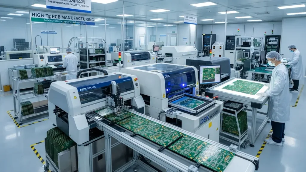
High-Tg PCB Manufacturing Facility and Automated Production Line
A qualified high‑Tg PCB manufacturer should evaluate the complete thermal and mechanical requirements of the PCB rather than selecting material based on Tg alone.
High‑Tg PCBs are commonly specified when a conventional FR‑4 system does not provide sufficient thermal margin, dimensional stability, or reliability for the intended application.
Typical requirements can include:
- Higher resistance to thermal cycling
- Compatibility with lead‑free assembly
- Improved dimensional stability
- Lower Z‑axis expansion
- Better resistance to delamination
- Improved CAF resistance where the selected material provides it
- Higher thermal reliability for multilayer construction
- Stable performance through repeated assembly or operating‑temperature exposure
However, Tg is not the maximum operating temperature of a PCB.
A high‑Tg material must be evaluated together with Td, CTE, T260/T288 behavior, moisture performance, dielectric requirements, copper adhesion, laminate construction, assembly profile, and the actual product temperature range.
That is why the first step at Hongda is an engineering review rather than simply assigning the highest available Tg material to every design.
Need help selecting the right laminate? Send your stackup or PCB files for an engineering review.
What High‑Tg PCB Materials Can We Manufacture?
High‑Tg PCB fabrication can use different FR‑4 and advanced laminate systems depending on the required Tg, thermal reliability, electrical performance, layer count, HDI structure, and application.
A practical material‑selection framework is:
| Material class | Typical Tg range* | Typical application direction |
|---|---|---|
| Standard FR‑4 | ~130°C class | General electronics |
| Mid‑Tg FR‑4 | ~150–160°C class | Higher thermal demand and lead‑free assembly |
| High‑Tg FR‑4 | ~170°C class and above | Automotive, industrial and high‑reliability multilayer PCBs |
| Advanced high‑Tg systems | Material‑specific | Severe thermal cycling and specialized applications |
| High‑Tg HDI materials | Material‑specific | Sequential lamination and high‑density interconnects |
*Actual Tg depends on the laminate manufacturer, resin system, construction, and test method.
High‑Tg FR‑4 is not one universal material specification. Different laminate systems can have substantially different values for CTE, Td, T260/T288, dielectric properties, moisture behavior, and processing characteristics.
For this reason, an RFQ should identify the required material family or performance requirements whenever the application has defined reliability criteria.
What Should Be Compared Besides Tg?
A material comparison should consider:
Tg → Td → Z‑axis CTE → T260/T288 → dielectric properties → moisture behavior → copper adhesion → CAF resistance → processing compatibility
For example, two laminates with similar Tg values may behave differently during multilayer lamination or thermal cycling.
The correct material is therefore the one that satisfies the complete application requirement—not necessarily the material with the highest Tg number.
Which High‑Tg PCB Tg Range Should You Specify?
The required Tg should be selected from the PCB’s assembly temperature, operating temperature, thermal cycling profile, layer structure, reliability target, and laminate qualification requirements.
A simple selection approach is:
Application Temperature → Assembly Profile → Thermal Cycling → Reliability Requirement → Material Data → Stackup → Manufacturing Qualification
For example, a PCB used in a conventional indoor electronics product may not require the same laminate system as an automotive controller exposed to repeated temperature cycling.
A high‑layer‑count PCB can also introduce additional thermal and mechanical concerns because repeated heating and cooling interact with plated holes, dielectric layers, copper planes, and the laminate’s Z‑axis expansion.
Hongda’s engineering review therefore considers the complete PCB construction before recommending a material.
Do not specify “Tg 170°C” as the only material requirement if your project has a detailed reliability specification. Instead, provide the required material datasheet, customer specification, or reliability target whenever available.
What High‑Tg PCB Manufacturing Capabilities Are Available?
Hongda supports high‑Tg PCB fabrication from engineering review and prototype production through multilayer, HDI, fine‑line, drilling, plating, surface finishing, electrical testing, and production manufacturing.
The manufacturing capability can include:
| Capability | Engineering application |
|---|---|
| Multilayer PCB | High‑density routing and power/ground structures |
| High‑Tg FR‑4 | Thermal and reliability requirements |
| HDI | High‑density interconnects |
| Blind/buried vias | Layer‑to‑layer interconnection |
| Laser microvias | HDI and fine‑pitch BGA escape |
| Mechanical drilling | Through‑hole structures |
| Fine‑line imaging | Dense routing |
| LDI | High‑precision circuit imaging |
| mSAP | Fine‑line applications where qualified |
| Controlled impedance | High‑speed signal requirements |
| Heavy copper | Higher‑current applications |
| AOI | Circuit defect inspection |
| X‑ray | Internal and hidden‑feature inspection |
| Electrical testing | Open/short verification |
| Microsection | Internal structure verification |
Hongda publicly describes multilayer and HDI production, laser microvias, LDI, high‑Tg FR‑4, and advanced inspection processes as part of its manufacturing technology portfolio.
The important distinction is that these technologies are not independent features. A demanding PCB may require several of them to operate together.
Can We Manufacture High‑Tg Multilayer and HDI PCBs?
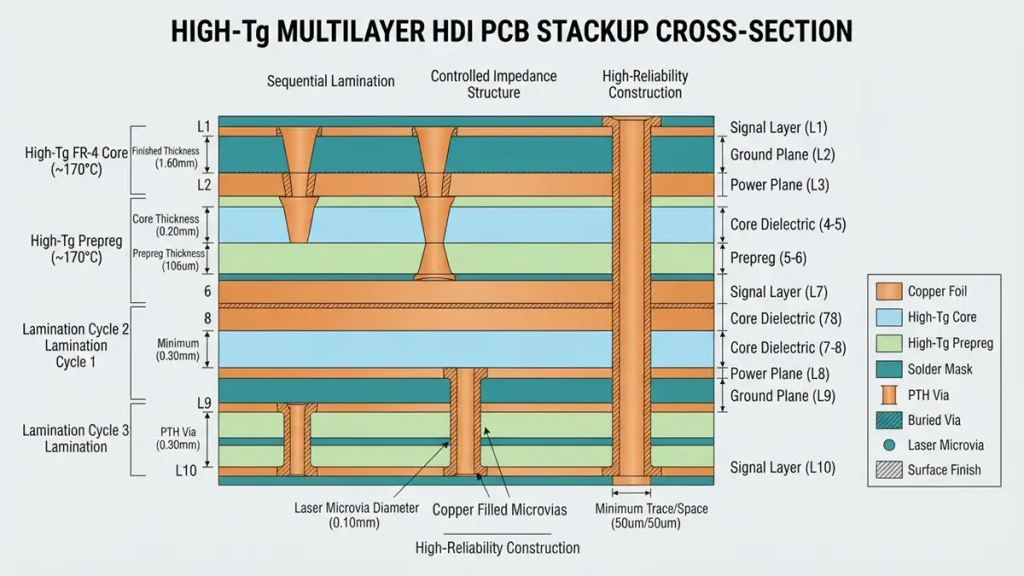
High-Tg Multilayer HDI PCB Stackup Cross-Section
Yes. High‑Tg multilayer PCB manufacturing can combine high‑Tg laminate systems with sequential lamination, blind and buried vias, laser microvias, fine‑line imaging, controlled impedance, and inspection processes according to the released design.
For complex boards, the critical manufacturing chain is:
Material → Stackup → Lamination → Registration → Drilling → Desmear → Plating → Imaging → Inspection
High‑Tg material alone does not solve registration or HDI manufacturing problems.
As layer count increases, dimensional movement during lamination becomes increasingly important. Fine‑pitch BGA structures, small annular rings, microvias, backdrilled vias, and controlled‑impedance routing can all reduce the available manufacturing margin.
For this reason, Hongda’s engineering review examines the relationship between:
- Layer count
- Core thickness
- Prepreg construction
- Copper distribution
- Via structure
- Registration
- Finished thickness
- Impedance
- Surface finish
- Reliability requirements
How Do We Control High‑Tg PCB Lamination and Registration?
High‑Tg multilayer lamination is controlled through qualified material construction, prepreg selection, stackup design, copper‑density evaluation, vacuum/press conditions, dimensional compensation, and post‑process inspection.
Lamination is one of the most important steps in high‑Tg PCB fabrication.
During pressing, resin softens, flows, wets the required surfaces, fills appropriate spaces, and then cures into the final dielectric structure.
The manufacturing challenge is controlled resin flow, not simply maximum resin flow.
Potential problems include:
- Resin starvation
- Excessive resin displacement
- Voids
- Layer misregistration
- Uneven dielectric thickness
- Warpage
- Poor interlayer bonding
- Local variation caused by copper‑density differences
A high‑Tg laminate may also require a process window different from a conventional FR‑4 system.
Therefore, the press cycle should be matched to the selected laminate and prepreg system rather than using one generic cycle for every PCB.
Why Does Copper Distribution Matter?
A multilayer PCB does not contain uniform copper across every layer.
One region may contain large power planes while another contains dense signal routing or relatively little copper.
These differences affect resin flow and local laminate construction during pressing.
For demanding boards, stackup engineering therefore considers:
Copper Pattern Density + Prepreg Construction + Resin Flow + Final Dielectric Thickness
This is especially important when controlled impedance or tight layer registration is required.
What Via Technologies Are Available for High‑Tg PCBs?
Depending on the design, high‑Tg PCBs can use through‑holes, blind vias, buried vias, laser microvias, via‑in‑pad, and sequential HDI structures.
Through‑Hole Vias
Used for conventional multilayer interconnection and component mounting.
Blind Vias
Connect an external layer to one or more internal layers without passing through the entire board.
Buried Vias
Connect internal layers and remain hidden within the multilayer structure.
Laser Microvias
Used for high‑density interconnects and fine‑pitch component escape routing.
Via‑in‑Pad
Useful for dense BGA layouts when properly filled, planarized, and qualified.
The selected via technology should be considered together with:
- Finished board thickness
- Copper thickness
- Aspect ratio
- Layer construction
- Pad size
- BGA pitch
- HDI sequence
- Plating requirements
- Reliability requirements
Hongda’s published capabilities include laser microvias and HDI structures for high‑density PCB applications.
What PCB Thickness and Copper Thickness Can We Support?
High‑Tg PCB thickness and copper requirements should be selected according to mechanical structure, current capacity, impedance, thermal performance, via design, and the manufacturing process.
Typical RFQ parameters include:
| Parameter | Engineering consideration |
|---|---|
| Finished thickness | Mechanical fit and stackup |
| Core thickness | Impedance and dielectric structure |
| Prepreg thickness | Lamination and dielectric spacing |
| Inner copper | Current capacity and plane construction |
| Outer copper | Current capacity and surface processing |
| Heavy copper | Power and high‑current applications |
| Minimum trace/space | Routing density |
| Hole diameter | Via and component requirements |
| Aspect ratio | Drill/plating reliability |
| Impedance | Signal‑integrity requirements |
Hongda also manufactures heavy‑copper PCB structures using high‑Tg FR‑4 and other specialized material systems for higher‑current applications.
For high‑current designs, copper thickness should not be selected independently from the thermal design and finished board thickness.
Which Surface Finishes Are Available for High‑Tg PCBs?
Surface finish should be selected according to solderability, pad geometry, assembly process, contact requirements, storage conditions, and product reliability.
Common options can include:
- ENIG
- ENEPIG
- HASL
- Lead‑free HASL
- OSP
- Immersion tin
For fine‑pitch BGA and HDI applications, surface flatness and pad geometry become particularly important.
For connector or repeated‑contact applications, the surface‑finish requirement can be different from that of a conventional SMT board.
The RFQ should therefore specify the surface finish rather than leaving the decision entirely to the fabricator.
How Do We Test and Inspect High‑Tg PCBs?
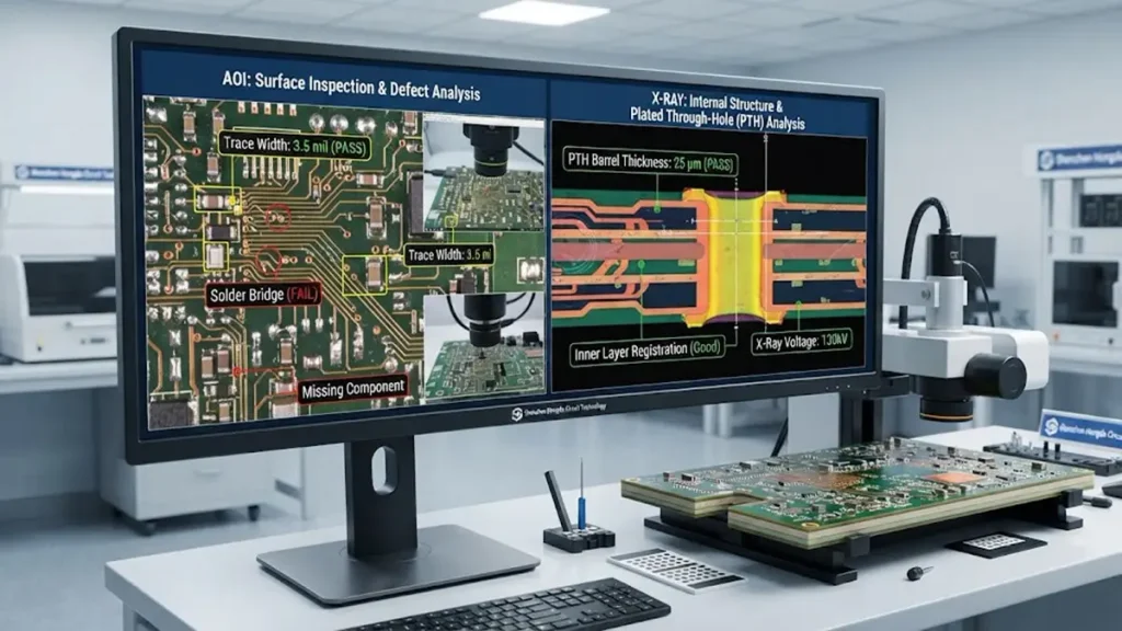
High-Tg PCB Quality Inspection with AOI and X-Ray Analysis
High‑Tg PCB quality should be verified through multiple inspection methods matched to the relevant manufacturing risks.
| Inspection | What it verifies |
|---|---|
| AOI | Circuit‑pattern defects |
| X‑ray | Hidden structures and internal registration |
| Electrical test | Opens and shorts |
| Microsection | Plated‑hole and internal structure |
| Impedance testing | Controlled‑impedance requirements |
| Dimensional inspection | Board and critical dimensions |
| Visual inspection | Surface workmanship |
| Reliability testing | Application‑specific thermal/mechanical performance |
No single test proves complete PCB reliability.
For example, electrical testing can identify opens and shorts but cannot replace a microsection when plated‑hole structure must be verified.
Likewise, AOI can detect visible circuit‑pattern defects but does not replace X‑ray inspection for selected hidden structures.
The inspection plan should therefore be connected to the failure mechanisms that matter to the application.
How Is High‑Tg PCB Reliability Evaluated?
Reliability evaluation should consider thermal expansion, plated‑hole integrity, delamination resistance, moisture exposure, thermal cycling, copper integrity, and the customer’s actual qualification requirements.
Important material and construction parameters may include:
- Tg
- Td
- Z‑axis CTE
- T260
- T288
- Moisture resistance
- CAF resistance
- Copper peel strength
- Dielectric properties
- Thermal cycling performance
A key engineering principle is:
High Tg is a material‑selection parameter, not a complete reliability qualification.
The final reliability of the PCB depends on the laminate, stackup, copper structure, drilling, plating, lamination, surface finish, assembly process, and operating environment.
For automotive, industrial, aerospace, medical, or other high‑reliability applications, customer‑specific qualification requirements should be reviewed before production.
What High‑Tg PCB Applications Do We Support?
High‑Tg PCB fabrication is suitable for applications where thermal exposure, repeated thermal cycling, assembly temperature, dimensional stability, or long‑term reliability create requirements beyond a basic PCB construction.
Potential applications include:
Automotive Electronics
Engine‑control, power‑control, sensing, communications, and other automotive electronics can require higher thermal and reliability performance.
Industrial Electronics
Industrial control equipment may experience continuous operation, temperature variation, vibration, and long service intervals.
Power Electronics
Higher copper weight, thermal management, and high‑Tg dielectric systems may be combined depending on current and temperature requirements.
Telecommunications
High‑layer‑count and high‑density boards may combine high‑Tg materials with controlled impedance and HDI structures.
Computing and AI Infrastructure
High‑density multilayer boards can require high‑Tg materials together with advanced stackups, fine‑line fabrication, controlled impedance, and thermal‑management considerations.
Medical and High‑Reliability Electronics
Material selection and process qualification become particularly important where long‑term reliability and regulatory requirements apply.
Application suitability must always be evaluated against the actual operating temperature, assembly process, electrical requirements, mechanical environment, and qualification standard.
Can We Manufacture High‑Tg PCB Prototypes Before Mass Production?
Yes. High‑Tg PCB prototype production can be used to validate material selection, stackup, manufacturability, drilling, registration, impedance, and inspection requirements before volume production.
A practical NPI process is:
Engineering Review → DFM → Material Confirmation → Prototype → Inspection → Customer Validation → Pilot Production → Mass Production
Prototype builds are particularly valuable when the design contains:
- High layer count
- New laminate
- Tight registration
- HDI
- Fine‑pitch BGA
- Controlled impedance
- Heavy copper
- Unusual thickness
- Customer‑specific reliability requirements
The objective of the prototype is not simply to prove that a board can be fabricated.
It should reduce manufacturing uncertainty before the production release.
How Does Our High‑Tg PCB Engineering Review Work?
Hongda reviews the PCB data, material requirements, stackup, fabrication constraints, testing requirements, and production quantity before finalizing the manufacturing quotation.
Step 1 — File Review
Gerber, ODB++, drill files, drawings, stackup, and specifications are reviewed.
Step 2 — Material Review
The requested Tg, laminate family, core, prepreg, resin system, and other material requirements are evaluated.
Step 3 — DFM Review
Critical line/space, holes, annular rings, registration, copper distribution, solder mask, and surface‑finish requirements are checked.
Step 4 — Manufacturing Assessment
Lamination, drilling, plating, HDI, surface finishing, and inspection requirements are evaluated.
Step 5 — RFQ
Pricing and lead time are prepared against the reviewed manufacturing specification.
Step 6 — Production
After customer approval, the released manufacturing data is transferred into production.
This engineering‑first workflow helps prevent a common procurement problem:
A PCB is quoted successfully, but the original design requirement was never fully evaluated for production.
Why Choose Shenzhen Hongda as Your High‑Tg PCB Supplier?
Shenzhen Hongda combines high‑Tg material engineering, multilayer PCB fabrication, HDI processing, precision imaging, laser drilling, inspection, and production support within one manufacturing workflow.
High‑Tg Material Engineering
Material selection is matched to thermal, electrical, mechanical, and reliability requirements.
Multilayer Manufacturing
High‑layer‑count PCB construction is supported for complex routing and power/ground architectures.
HDI and Microvia Processing
Laser‑drilled microvias and sequential HDI structures can be integrated into high‑density designs.
Precision Imaging
LDI and advanced imaging processes support fine‑line and registration‑sensitive PCB fabrication.
Quality Inspection
AOI, X‑ray, electrical testing, dimensional inspection, and microsection analysis can be incorporated according to project requirements.
Prototype to Production
The manufacturing workflow supports engineering builds, prototypes, pilot production, and volume manufacturing.
Engineering RFQ Review
Customers can submit the PCB data and receive an engineering assessment before production quotation.
Hongda’s published technology portfolio includes high‑Tg FR‑4, multilayer and HDI manufacturing, laser microvias, LDI, fine‑line processing, and automated inspection capabilities.
What Should You Include in a High‑Tg PCB RFQ?
The more complete the RFQ data, the more accurately a manufacturer can evaluate material compatibility, manufacturability, cost, and lead time.
PCB Information
- PCB type
- Layer count
- Board dimensions
- Finished thickness
- Thickness tolerance
- Inner copper thickness
- Outer copper thickness
- Minimum line/space
- Minimum finished hole
- Drill information
Material Requirements
- High‑Tg requirement
- Target Tg
- Preferred laminate
- Customer‑approved material list
- Td requirement
- CTE requirement
- CAF requirement
- Halogen‑free requirement if applicable
Electrical Requirements
- Controlled impedance
- Single‑ended impedance
- Differential impedance
- Impedance tolerance
- High‑speed requirements
Manufacturing Requirements
- HDI
- Blind/buried vias
- Microvias
- Via‑in‑pad
- Backdrilling
- Copper filling
- Surface finish
- Solder mask
Quality Requirements
- IPC class
- AOI
- X‑ray
- E‑test
- Microsection
- Reliability testing
- Customer‑specific qualification
Commercial Information
- Prototype quantity
- Production quantity
- Target delivery
- Annual volume
- Destination
- Packaging requirement
The most useful files to sThe most useful files to submit are Gerber/ODB++, drill files, stackup, fabrication drawing, material specification, and testing requirements. See also the full RFQ checklist for glass‑based PCB designs in Glass PCB: what should a glass PCB RFQ include.ubmit are Gerber/ODB++, drill files, stackup, fabrication drawing, material specification, and testing requirements.
High‑Tg PCB Manufacturer FAQ
Can you manufacture high‑Tg FR4 PCBs with custom stackups?
Yes. High‑Tg FR‑4 can be incorporated into custom multilayer stackups according to the required layer count, finished thickness, copper distribution, impedance, via structure, and material specification.
What high‑Tg PCB materials and Tg ranges can you supply?
Material availability depends on the required construction and project specification. High‑Tg FR‑4 systems are available across different Tg classes, while exact values must be confirmed against the selected laminate manufacturer’s datasheet and test method.
Can you manufacture high‑Tg multilayer and HDI PCBs?
Yes. High‑Tg multilayer PCB manufacturing can be combined with HDI, blind and buried vias, laser microvias, fine‑line imaging, controlled impedance, and application‑specific inspection.
Can you provide high‑Tg PCB prototypes before mass production?
Yes. Prototype builds can be used to validate material selection, stackup, registration, drilling, plating, impedance, and other manufacturing requirements before production release.
What information do you need to quote a high‑Tg PCB?
The most useful information includes Gerber or ODB++ files, drill files, layer count, dimensions, thickness, copper weight, material/Tg requirement, minimum line/space, hole size, via technology, surface finish, testing requirements, quantity, and delivery target.
Request a High‑Tg PCB Quote
Whether you need a high Tg PCB prototype, high Tg multilayer PCB, high Tg HDI PCB, or production‑volume high‑temperature PCB, Hongda can review your design and manufacturing requirements before quotation.
Send your PCB data for an engineering review covering: Material → Stackup → DFM → Lamination → Drilling → Plating → Inspection → Production
Request a High‑Tg PCB Quote Shenzhen Hongda Circuit Technology Co., Ltd. Email: pcb@pcbkr.com Website: www.pcbkr.com
About Author
David Chen https://www.linkedin.com/in/pcbcoming
David Chen boasts an extensive professional background in PCBA manufacturing, PCBA testing, and PCBA optimization, with specialized expertise in high-precision PCBA fault analysis and rigorous PCBA reliability testing. The author has worked with high-layer-count server PCB fabrication, ultra-low-loss backplane stackups, and thermo-mechanical reliability optimization for AI infrastructure projects involving 112G and 224G PAM4 architectures. Skilled in complex circuit design and cutting-edge advanced PCB manufacturing processes, he delivers solutions that elevate product durability and performance across industrial applications. His technical articles focusing on PCBA manufacturing workflows and testing methodologies are widely cited by industry peers, research institutions, and technical platforms, solidifying his reputation as a recognized technical authority in the global circuit board manufacturing sector.