4 Layer PCB Prototype Manufacturer in China: Fast, Reliable Prototypes for Engineering Validation
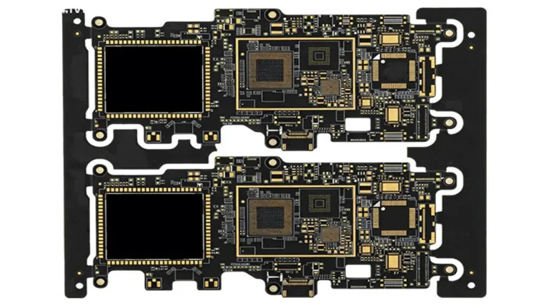
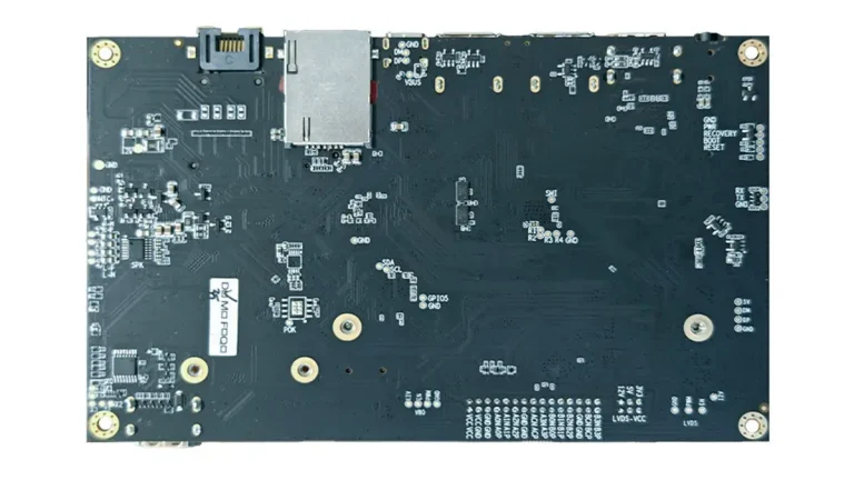
4 layer PCB prototypes are our core customized manufacturing solutions delivered in China, tailored to meet clients’ demands for engineering validation, functional testing and low-volume production needs. We support diverse high-quality board materials, including standard FR-4 and premium selected high-Tg materials to adapt to different working environment and performance requirements of electronic products.
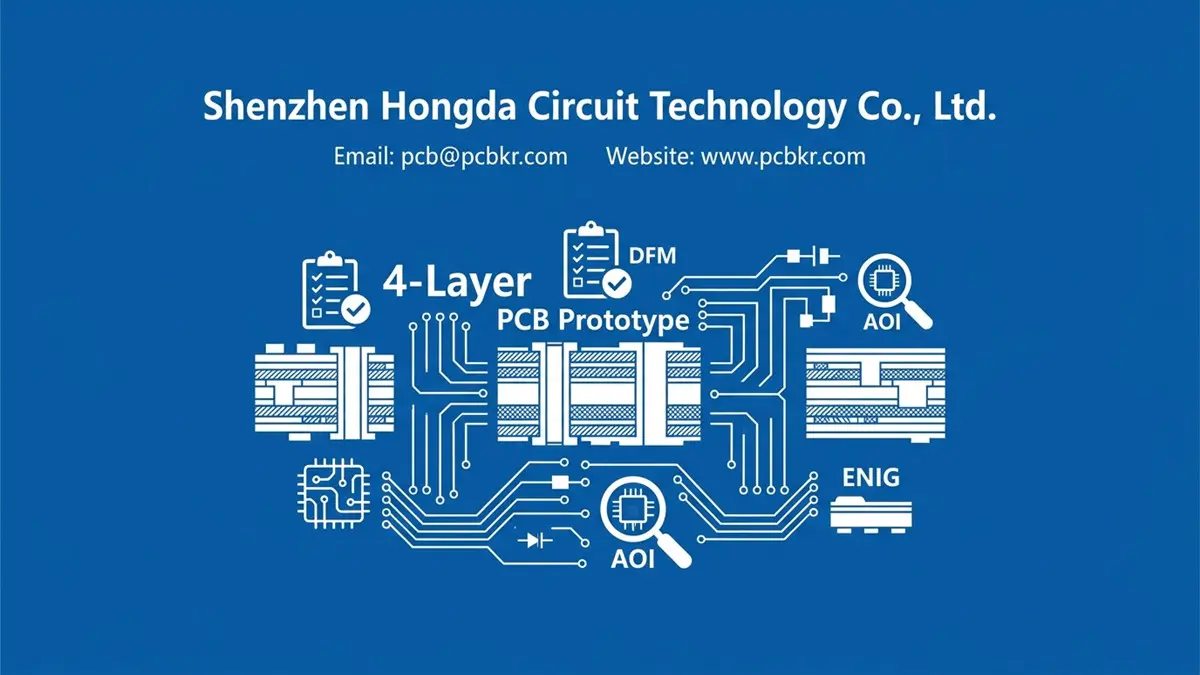
Our comprehensive 4-layer PCB manufacturing service integrates full-process professional technologies and quality control. We provide precise controlled impedance processing, reliable plated through hole fabrication, and multiple mainstream surface finish options such as HASL and ENIG to ensure the stability, solderability and durability of PCBs. In addition, strict electrical testing and professional DFM review are included in our standard service to eliminate potential design and manufacturing risks. We also offer optional one-stop PCB assembly service to further simplify clients’ procurement and product development procedures.
We accommodate flexible order quantities ranging from single engineering samples to small-scale production batches. Before formal fabrication, our professional technical team will conduct a detailed review of your Gerber files, verify and confirm the PCB stack-up structure, and provide a clear, itemized quotation for your reference, ensuring full transparency of every production detail and cost.
Upload your Gerber files to receive a technical review and itemized quotation. Email: pcb@pcbkr.com
Why Use a 4-Layer PCB Prototype?
What Is a 4-Layer PCB?
A 4-layer PCB is a printed circuit board built from four conductive copper layers separated by dielectric material. A common configuration uses a top signal layer, a ground or power plane, a second power or ground plane, and a bottom signal layer. This arrangement is a useful starting point, but it is not the only valid structure — the actual stack-up should be adjusted based on impedance targets, EMI control, thermal design, and component density. Before fabrication, your stack-up should be confirmed with the manufacturer rather than assumed from a generic diagram.
Advantages of Four-Layer Prototypes
Compared with a two-layer board, a four-layer prototype typically offers:
- Better power and ground integrity through dedicated plane layers
- Easier implementation of controlled impedance for high-speed interfaces
- Shorter return paths for high-speed signals
- Reduced EMI and crosstalk risk
- Support for higher component density
- A validation platform that carries lessons forward into six-layer or HDI designs
- A practical balance between performance, cost, and development schedule
When Should You Choose Four Layers Instead of Two?
| Requirement | 2-layer PCB | 4-layer PCB |
|---|---|---|
| Simple low-speed circuits | Often sufficient | May be unnecessary |
| Ground-plane continuity | Limited | Better |
| USB, Ethernet, CAN or other high-speed interfaces | More difficult | Generally easier |
| Compact component placement | Limited | Better routing flexibility |
| EMI control | Requires careful layout | More design options |
| Prototype cost | Lower board cost | Higher fabrication cost |
Choosing four layers does not automatically guarantee high-speed performance. The result still depends on stack-up, layer spacing, reference planes, impedance calculation, and routing practice — layer count is one input among several.
Our 4-Layer PCB Prototype Capabilities
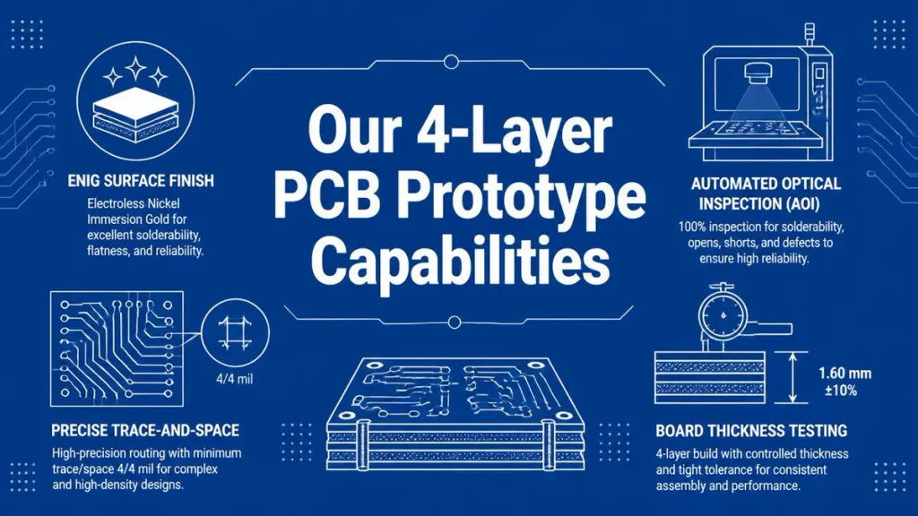
Our 4-Layer PCB Prototype Manufacturing Capabilities – Shenzhen Hongda Circuit
Standard Manufacturing Specifications
| Parameter | Standard Option | Custom Option |
|---|---|---|
| Layer count | 4 layers | Customized multilayer |
| Base material | FR-4 | High-Tg FR-4, halogen-free, selected high-frequency materials |
| Board thickness | 1.6 mm typical | Custom thickness |
| Copper weight | 1 oz typical | Custom outer and inner-layer copper |
| Minimum trace/space | Confirmed at quotation | Subject to stack-up and copper thickness |
| Minimum finished hole | Confirmed at quotation | Engineering review required |
| Surface finish | HASL, lead-free HASL, ENIG | OSP, immersion tin, other qualified finishes |
| Solder mask | Green, other colors | Custom color subject to availability |
| Impedance control | Available where specified | Stack-up and impedance table required |
| Testing | Electrical test, visual inspection | AOI, X-ray, additional tests where applicable |
| Quantity | Prototype and low volume | Production quantities |
Capability figures are confirmed against our own production data at the time of quotation rather than quoted from industry averages, since actual trace/space, hole size, and tolerance depend on the specific stack-up and copper weight ordered.
Materials
- Standard FR-4 — suitable for general control circuits and embedded electronics; a cost-effective default for most prototypes.
- High-Tg FR-4 — recommended where the board will see higher thermal exposure or a lead-free assembly profile; typically carries a moderate cost premium.
- Halogen-free laminates — used where environmental or customer compliance requirements call for halogen-free construction.
- High-frequency laminates — used for RF or high-speed applications where signal loss and dielectric consistency matter more than cost.
- Hybrid stack-ups — combine two or more materials in the same board; these require additional engineering confirmation before quotation.
For each material family, confirm the target application, expected cost impact, and any manufacturing considerations — including whether a specific material brand or grade needs to be locked in before production.
Surface Finishes
| Finish | Suitable For | Main Consideration |
|---|---|---|
| HASL | Cost-sensitive general prototypes | Surface flatness is lower than ENIG |
| Lead-free HASL | RoHS-oriented products | Higher process temperature |
| ENIG | Fine-pitch components and prototype testing | Higher cost; nickel/gold thickness control matters |
| OSP | Flat pads and selected SMT applications | Handling and shelf-life considerations |
| Immersion tin | Certain fine-pitch designs | Storage and process control required |
Special Processes
Beyond standard fabrication, engineering review can support processes such as blind and buried vias, via-in-pad, heavy copper, edge plating or castellated holes, and controlled dielectric thickness for specific impedance targets. Each of these should be discussed at the RFQ stage, since they affect both cost and lead time.
4-Layer PCB Stack-Up and Impedance Control
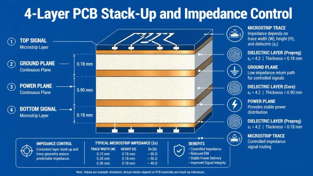
4-Layer PCB Stack-Up and Impedance Control Diagram – Shenzhen Hongda Circuit
Typical Four-Layer Stack-Ups
Below are two representative examples. They illustrate common approaches, not a fixed template — your actual stack-up should be confirmed against your design requirements before production.
Example A: General digital board
| Layer | Function |
|---|---|
| L1 | Components and high-speed signals |
| L2 | Solid ground plane |
| L3 | Power and low-speed routing |
| L4 | Signals and selected components |
Example B: Impedance-controlled board
| Layer | Function |
|---|---|
| L1 | Critical signals |
| L2 | Continuous reference plane |
| L3 | Power/reference plane |
| L4 | Secondary signals |
Controlled-Impedance Design
Impedance is determined by trace width, trace spacing, copper thickness, dielectric thickness, and the dielectric constant (Dk) of the chosen material. Changing the board thickness or the spacing between layers will change the resulting impedance, even if every other parameter stays the same. It is not enough to specify “impedance control required” — the RFQ should state the target impedance and the interface type (single-ended or differential), so the stack-up can be engineered to match. The stack-up should be confirmed before quotation and production, not adjusted afterward as a correction.
Common controlled-impedance interfaces we support review for:
- USB 2.0 and USB 3.x
- Ethernet
- PCIe-related designs, where the layer stack-up is suitable
- LVDS
- CAN and RS-485
- DDR and memory interfaces
- RF or antenna feed lines
Not every four-layer board is automatically suitable for PCIe, DDR5, or high-speed serial protocols such as 224G PAM4. For demanding high-speed applications, we recommend an engineering evaluation of material selection, insertion loss, via structure, reference-plane continuity, and simulation requirements before committing to a stack-up.
Design Rules That Affect Cost and Yield
The following design choices influence both manufacturability and price:
- Very narrow trace/space
- Small finished hole sizes
- High aspect-ratio vias
- Heavy copper on thin boards
- Tight annular rings
- Via-in-pad and filled vias
- Edge plating or castellated holes
- Large copper areas and thermal imbalance
- Slots, countersinks, and unusual routing profiles
- Tight impedance tolerance
Before submitting design files, check:
- Gerber and drill files match the current design revision
- Board outline and drill file are consistent
- Stack-up, material, and thickness are specified
- Impedance targets and interface types are stated, if applicable
- Minimum trace/space and hole sizes are within the confirmed capability range
- Copper weight is specified for each layer
- Surface finish and solder mask color are specified
- Panelization requirements, if any, are noted
- Any special processes (blind/buried vias, heavy copper, edge plating) are called out separately
4-Layer PCB Prototype Cost
Cost Factors
The price of a 4-layer PCB prototype depends on a combination of variables rather than layer count alone:
- Board dimensions
- Quantity
- Number of unique designs
- Material and Tg
- Finished board thickness
- Inner and outer copper weight
- Minimum trace/space and hole size
- Surface finish
- Solder mask color
- Impedance control
- Electrical testing
- Panelization
- Special processes
- Shipping destination and Incoterms
- PCB assembly and component sourcing
What Is Included in a Quote?
Online “starting prices” can be misleading because they often apply only to a specific size, quantity, material, and delivery schedule. Shipping, engineering fees, testing fees, and assembly costs may be calculated separately, and quoting practices differ between suppliers. The most reliable way to compare manufacturers is to request quotes using the same Gerber files, the same lead time, and the same quality requirements — so you are comparing equivalent scopes of work rather than different starting points.
Information Needed for an Accurate RFQ
To receive an accurate, itemized quotation, please provide:
- Gerber or ODB++ files
- Drill files
- Board outline
- Stack-up requirement
- Quantity and number of designs
- Material and thickness
- Copper weight
- Surface finish
- Solder mask and silkscreen colors
- Impedance requirements
- Electrical testing requirements
- Delivery destination
- Required date
- PCBA BOM and centroid files, if assembly is needed
Upload your Gerber files to receive a technical review and itemized quotation. Email:pcb@pcbkr.com
4-Layer PCB Prototype Lead Time
Production Schedule
Rather than quoting a single number such as “24 hours” or “3–5 days,” it is more useful to understand what actually happens between order confirmation and shipment:
- File upload and quotation
- DFM and engineering review
- Material confirmation
- Lamination and imaging
- Drilling, plating, and etching
- Solder mask, surface finish, and routing
- Electrical testing and final inspection
- Packing and international shipment
Causes of Delay
Common factors that extend a prototype schedule include:
- Incomplete Gerber or drill files
- Conflicting design files
- Late stack-up approval
- Special material availability
- Tight impedance tolerance
- Via-in-pad or HDI requirements
- Panelization changes
- Component shortages for PCBA
- Customs or destination-country shipping issues
Prototype, Pilot and Production Lead Times
It is worth distinguishing between:
- Prototype lead time — fabrication of a small engineering sample quantity
- Pilot-run lead time — a validation batch ahead of full production
- Mass-production lead time — scheduled volume manufacturing
- Transit time — shipping from the factory to your destination
We provide a typical lead time range for each stage and specify the point at which the clock starts (for example, from design approval or from material confirmation), rather than a fixed promise that does not account for design complexity.
Our 4-Layer PCB Prototype Manufacturing Process
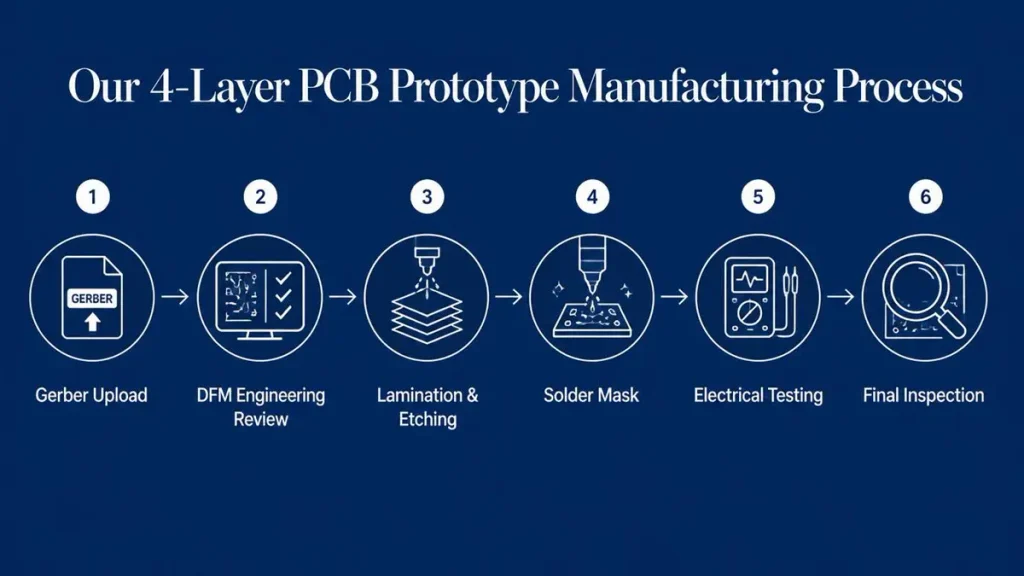
4-Layer PCB Prototype Manufacturing Process Step-by-Step – Shenzhen Hongda Circuit
- Upload Gerber and technical files — you submit design and specification files for review.
- Engineering review and DFM feedback — our team checks manufacturability and flags any issues.
- Stack-up and material confirmation — layer structure, material, and thickness are finalized.
- Quote approval and production scheduling — you approve the itemized quote and the job is scheduled.
- Inner-layer imaging and etching — the inner circuit patterns are formed.
- Lamination and drilling — layers are bonded and through-holes are drilled.
- Plating and outer-layer imaging — holes are plated and outer circuit patterns are formed.
- Solder mask, surface finish, and profiling — solder mask is applied, finish is added, and the board is routed to shape.
- AOI and electrical testing — automated optical inspection and electrical testing check for defects and continuity.
- Final inspection, packing, and shipment — boards are inspected, packed, and shipped.
- Optional PCB assembly and functional testing — components are placed and the assembled board is tested, if PCBA is requested.
At each stage, we confirm the required input files, the key quality-control checkpoint, anything that needs your sign-off, and the resulting output — so you know exactly where your order stands.
DFM Review and Engineering Support
DFM Checks
Before production, our engineers review your files for:
- Clearance and copper spacing
- Drill-to-copper clearance
- Annular ring
- Solder mask expansion
- Acid traps
- Copper balance
- Plane voids and thermal relief
- Silkscreen-to-pad clearance
- Edge clearance
- Hole plugging requirements
- Panel utilization
- Impedance feasibility
- Manufacturing tolerances
Typical Design Issues
Examples of the kind of feedback a DFM review can surface:
- “The requested 3 mil trace/space is not compatible with the specified 2 oz copper; we recommend a revised stack-up.”
- “The target 50 Ω microstrip requires a different dielectric thickness.”
- “The via-to-copper clearance should be increased to reduce plating risk.”
- “The selected ENIG finish is suitable for the fine-pitch BGA pads.”
Engineering Review Versus Automated Quote
| Automated Quote | Engineering DFM Review |
|---|---|
| Fast initial price | Checks design manufacturability |
| Based on entered parameters | Reviews actual Gerber and drill files |
| May miss application-specific risks | Identifies process and reliability risks |
| Useful for rough comparison | Better before production approval |
We recommend using an automated quote for an initial budget estimate, and an engineering DFM review before final production approval.
Manufacturing, Testing and Quality Control
Inspection and Electrical Testing
Depending on the order, quality controls can include:
- Incoming material inspection
- Inner-layer AOI
- Lamination inspection
- Plating thickness verification
- Outer-layer AOI
- Solder mask inspection
- Surface-finish inspection
- Electrical test
- Final visual inspection
- Dimensional inspection
- Microsection analysis for qualified orders
IPC, RoHS, REACH and Quality Documentation
Relevant standards and references include:
- IPC-A-600 — acceptability of bare printed boards
- IPC-6012 — qualification and performance specification for rigid PCBs
- IPC-A-610 — acceptance of electronic assemblies
- Class 2 versus Class 3 acceptance requirements
- RoHS and REACH documentation, where applicable
- UL marking or certification, where applicable
Any statement about the acceptance class we build to — for example “built to IPC Class 2” with “Class 3 available upon request” — reflects our actual quality system and is confirmed rather than assumed.
Documents Customers Can Request
- Certificate of Conformance
- Material certificate
- Test report
- Impedance report
- Microsection report
- RoHS/REACH declaration
- UL-related documentation
- Packing list and commercial invoice
- First article inspection report
4-Layer PCB Prototype Applications
Industrial and Embedded Electronics
Industrial control and automation, embedded controllers, and IoT gateways benefit from a four-layer board’s ability to manage ground planes more predictably and support denser component placement in compact enclosures.
Networking and High-Speed Devices
Networking and communication equipment, robotics, and smart devices often need the improved EMI control and high-speed interface routing that a four-layer stack-up makes easier to achieve.
Automotive, Medical and Other Applications
Power management and battery systems, automotive electronics, medical and instrumentation equipment, LED and display control, and — subject to qualification requirements — aerospace or defense-related electronics all draw on four-layer boards to provide a structure closer to production intent for functional and EMC testing.
Across these applications, the shared reasons to choose four layers are consistent: easier ground-plane management, support for denser components, better EMI control, improved high-speed interface routing, and a prototype structure that more closely resembles the final production board.
From Prototype to Low-Volume Production
Pilot Run Support
Once a prototype is validated, we can support:
- Design review
- Prototype fabrication
- Assembly prototype
- Functional testing
- Design revision support
- Panelization optimization
- Pilot production
- Production test fixtures
- BOM and approved vendor list review
- Consistency monitoring
Assembly and Functional Testing
If PCB assembly is required, our team can source components, perform SMT and THT assembly, and carry out functional testing before final packaging — with the scope of bare-board fabrication versus turnkey assembly clearly separated in the quotation.
What Changes When Scaling Up?
Moving from prototype to volume production shifts the focus toward material procurement, panel utilization, yield management, process capability, test coverage, incoming inspection, packaging, delivery scheduling, and engineering change control.
Production Transfer Checklist
| Stage | Customer Approval |
|---|---|
| Prototype | Gerber, stack-up and material |
| Validation | Electrical and functional test |
| Pilot run | Yield, dimensional and assembly review |
| Production | Control plan, test procedure and delivery schedule |
Why Choose Our China PCB Prototype Service?
Working with a China-based manufacturer can offer real advantages, including competitive manufacturing cost, a broad material and process supply chain, flexibility for prototype and low-volume orders, integrated fabrication and assembly under one roof, export packaging and logistics support, English-language engineering communication, the ability to consolidate multiple PCB designs into one order, and support through the transition from prototype to production.
At the same time, these are worth verifying with any supplier you are evaluating:
- Does the company operate its own production lines, or is it a trading intermediary?
- Is the quotation coming from the factory or from a trading company?
- Is there an English-speaking engineering team available for technical discussion?
- How are quality issues handled if they arise?
- Are small-batch orders genuinely accepted?
- Is there a second supplier or material alternative if something falls through?
- Can the company sign an NDA?
- Does the company support customer audits or factory visits?
We answer each of these directly, because a “China manufacturer” claim should be a starting point for supplier evaluation, not just a geographic keyword.
Frequently Asked Questions
Technical FAQs
What is a 4-layer PCB prototype?
A 4-layer PCB prototype is an engineering sample made with four conductive copper layers separated by dielectric material. It normally includes two outer signal layers and two internal power or ground layers, although the exact stack-up depends on routing, impedance, EMI, and thermal requirements.
What is the typical 4-layer PCB stack-up?
A common stack-up uses signal-ground-power-signal layers. However, the best configuration depends on the required impedance, board thickness, copper weight, signal speed, and power-distribution design.
Is a 4-layer PCB better than a 2-layer PCB?
A four-layer PCB generally provides more routing space, better ground-plane continuity, and more options for impedance and EMI control. A two-layer PCB may still be more economical for simple, low-speed circuits.
Can you manufacture impedance-controlled 4-layer PCBs?
Yes, provided the required impedance values, stack-up, material data, trace geometry, and tolerance are confirmed before production. The manufacturer should verify the design against the selected material and layer structure.
Can a 4-layer PCB support USB, Ethernet, CAN or LVDS?
It can support these interfaces when the stack-up, reference planes, routing geometry, return paths, termination, and design rules are appropriate. Layer count alone does not guarantee signal-integrity performance.
What materials are available for 4-layer prototypes?
Common choices include standard FR-4, high-Tg FR-4, halogen-free materials, and selected high-frequency laminates. The correct material depends on operating temperature, signal loss, compliance requirements, and assembly process.
Can you manufacture 4-layer PCBs with blind vias or microvias?
Some four-layer designs can use blind vias or microvias, but these processes require additional engineering review and may increase cost and lead time. Via structure, aspect ratio, pad design, and filling requirements should be specified in the RFQ.
What surface finish is best for a 4-layer prototype?
HASL is often selected for cost-sensitive general prototypes, while ENIG is useful for fine-pitch SMT, BGA pads, and a flatter surface. The appropriate finish depends on component pitch, soldering process, storage conditions, and budget.
Cost and Lead-Time FAQs
How much does a 4-layer PCB prototype cost?
The price depends on board size, quantity, material, thickness, copper weight, minimum trace and hole size, surface finish, testing, special processes, shipping, and assembly. An accurate quotation requires the Gerber and drill files rather than only the layer count.
What is the minimum order quantity for a 4-layer PCB prototype?
Prototype suppliers may accept very small quantities, but the practical minimum depends on the manufacturer’s process, setup costs, panelization, and production schedule. Request pricing for both the prototype quantity and a pilot quantity to compare the cost curve.
How long does a 4-layer PCB prototype take?
Lead time depends on design complexity, material availability, engineering approval, testing, and shipping. Ask the manufacturer to separate fabrication time from transit time and to define when the lead-time clock starts.
Can I get a fast-turn 4-layer PCB prototype?
Yes, fast-turn service may be available for standard materials and uncomplicated designs. Special materials, impedance control, HDI, unusual copper weights, tight tolerances, and assembly can extend the schedule.
Why is my 4-layer PCB quote higher than the advertised price?
Advertised prices may apply only to standard dimensions, quantities, materials, finishes, and delivery conditions. Engineering fees, testing, special processes, shipping, and PCBA may be quoted separately.
Procurement FAQs
What files are needed to quote a 4-layer PCB prototype?
Provide Gerber files, drill files, board outline, stack-up requirements, material, thickness, copper weight, surface finish, solder mask color, impedance requirements, quantity, and delivery destination. For assembly, also provide the BOM, centroid file, and assembly drawings.
How do I compare 4-layer PCB manufacturers in China?
Compare technical capability, actual factory location, DFM process, quality standards, test coverage, lead time, communication, quotation transparency, export experience, IP protection, and prototype-to-production support — not only unit price.
Is a China PCB prototype manufacturer suitable for international buyers?
A qualified Chinese manufacturer can be suitable when it provides clear specifications, responsive engineering communication, documented quality controls, secure file handling, export logistics, and transparent commercial terms. Customers should verify the factory and request samples or references when appropriate.
Do you sign an NDA before receiving Gerber files?
Yes — we can explain how design files are transferred, who can access them, how revisions are controlled, and whether an NDA is available, based on our actual file-handling policy.
Can you provide PCB assembly with the prototype?
If PCBA is available, we clarify whether the service includes component sourcing, SMT, THT, programming, AOI, X-ray, functional testing, and final packaging — clearly distinguishing bare-board fabrication from turnkey assembly.
Can you support the transition from prototype to mass production?
A capable supplier should be able to support DFM changes, pilot runs, panelization, yield review, test procedures, approved materials, revision control, and production scheduling. Ask whether the prototype line and mass-production line use compatible processes.
What happens if the prototype fails inspection?
The supplier should explain its nonconformance process, the evidence required from the customer, root-cause analysis, replacement or rework policy, and responsibility for shipping or remake costs.
Request a 4-Layer PCB Prototype Quote
Ready to move forward? Choose the path that fits where you are:
- Upload Gerber Files — get a technical review and an itemized quotation.
- Request a 4-Layer PCB Quote — provide your specifications for a fast estimate.
- Ask an Engineer to Review Your Design — get DFM feedback before you commit to production.
Not ready to upload files yet? You can also:
- Download the RFQ Checklist
- Request a Sample Specification
- Compare 4-Layer PCB Materials
- Talk to a PCB Engineer
- Request a Stack-Up Recommendation
What happens after you submit a request: your files are reviewed by our engineering team, checked against manufacturability requirements, and returned with an itemized quotation and any DFM feedback. If you need confidentiality, we can discuss file-handling procedures and an NDA before you share design data. If you’d like to talk through your stack-up or interface requirements first, we’re glad to set up an engineering discussion before you submit final files.
About Author
David Chen https://www.linkedin.com/in/pcbcoming
David Chen boasts an extensive professional background in PCBA manufacturing, PCBA testing, and PCBA optimization, with specialized expertise in high-precision PCBA fault analysis and rigorous PCBA reliability testing. The author has worked with high-layer-count server PCB fabrication, ultra-low-loss backplane stackups, and thermo-mechanical reliability optimization for AI infrastructure projects involving 112G and 224G PAM4 architectures. Skilled in complex circuit design and cutting-edge advanced PCB manufacturing processes, he delivers solutions that elevate product durability and performance across industrial applications. His technical articles focusing on PCBA manufacturing workflows and testing methodologies are widely cited by industry peers, research institutions, and technical platforms, solidifying his reputation as a recognized technical authority in the global circuit board manufacturing sector.