HDI PCB Prototype Manufacturer for Complex, High-Density Designs
Custom HDI PCB Prototypes for Engineering Validation
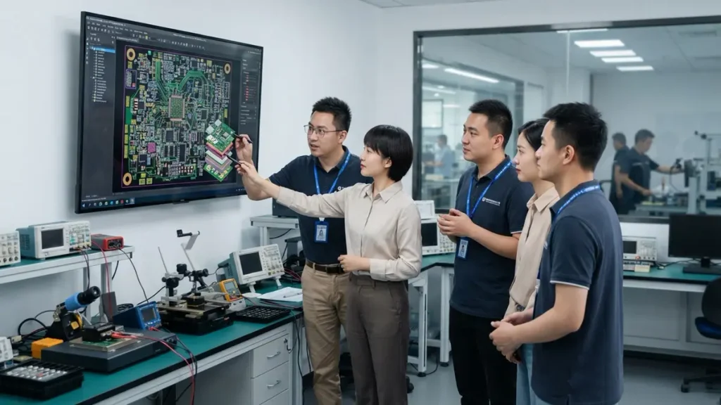
Hongda Circuit(PCBKR) engineering team reviewing a detailed digital layout and 3D stackup of an advanced HDI PCB prototype in a modern electronics laboratory
Shenzhen Hongda Circuit Technology Co., Ltd. manufactures custom High‑Density Interconnect (HDI) PCB prototypes for engineering teams that need to validate electrical performance, mechanical fit, and manufacturing feasibility before committing to volume production. Our service covers design review, fabrication, testing, and delivery — with a clear, documented path from prototype approval to production transfer.
We accept design data in Gerber, ODB++, IPC‑2581, or native CAD formats. Whether you are qualifying a fine‑pitch BGA layout, a stacked‑microvia stackup, or a high‑speed backplane segment, our engineering team reviews your files before fabrication begins, so manufacturability risks are identified early rather than discovered after the first prototype run.
Upload Your HDI PCB Files for Engineering Review → pcb@pcbkr.com
Why Choose Shenzhen Hongda Circuit Technology for HDI PCB Prototypes?
Buyers sourcing HDI prototypes are not looking for generic claims — they need outcomes they can measure against their own project risk. Our service is built around the outcomes that matter to procurement and design engineering teams alike:
- Early detection of DFM and DRC risks through a dedicated engineering review step, before CAM release.
- Stable microvia formation and sequential‑lamination control, supported by laser direct imaging (LDI) and precision laser‑drilling equipment.
- Shorter prototype iteration cycles, with engineering clarification handled in parallel with material preparation where possible.
- Tighter control of impedance, layer‑to‑layer registration, and copper distribution across dense HDI stackups.
- Direct communication between our engineering, quotation, and production planning teams, so purchasing contacts are not relayed through multiple intermediaries.
- A documented manufacturing path from prototype qualification to repeat and mass production, using the same approved stackup and process window.
This combination — technical review, process control, and production continuity — is what separates a prototype “run” from a prototype that is actually production‑representative.
The Role of Advanced Manufacturing Equipment in HDI PCB Quality
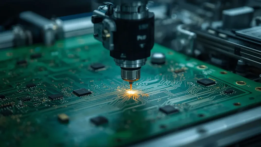
High-tech industrial laser drilling machine performing precision microvia formation on a multi-layer green circuit board during HDI PCB prototype manufacturing.
HDI PCB reliability is largely determined by the equipment used to form microvias, image fine circuitry, and control registration through multiple lamination cycles. Shenzhen Hongda Circuit Technology invests in production equipment aligned with current HDI manufacturing technology, including:
- CO₂ and UV laser drilling systems for microvia formation, supporting fine microvia diameters with controlled taper and copper‑capture‑pad geometry.
- Laser Direct Imaging (LDI) for inner‑ and outer‑layer circuitry, improving line‑width control and layer‑to‑layer registration compared to conventional phototool imaging — a key requirement for fine‑pitch BGA fanout and controlled‑impedance nets.
- Automated Optical Inspection (AOI) at inner‑layer and outer‑layer stages, to catch open/short and etching defects before lamination locks them into the stackup.
- X‑ray and flying‑probe electrical test equipment, used to verify buried‑via alignment and net continuity on completed boards.
- Vacuum lamination presses with process monitoring, supporting multiple sequential‑lamination cycles required for 1+N+1, 2+N+2, and any‑layer HDI structures.
- Plating lines capable of via‑fill and copper‑capping processes, supporting via‑in‑pad and stacked‑microvia designs used in dense BGA fanout.
These capabilities are not marketing abstractions — they directly determine which HDI structures, microvia diameters, and BGA pitches a manufacturer can realistically support at prototype scale without sacrificing repeatability when the design moves into production. We qualify each new HDI structure internally before offering it for customer prototypes, and we are glad to share process documentation relevant to your specific design during the engineering review stage.
Note: Actual equipment capability and qualified process windows should be confirmed against your specific design geometry, material selection, and layer count during the RFQ and DFM review process.
HDI PCB Prototype Capabilities
Use the table below as a starting reference. Final capability confirmation depends on your specific design geometry, material choice, layer count, and target yield — our engineering team will confirm exact limits during DFM review.
| Capability | Information Provided |
|---|---|
| HDI structures | 1+N+1, 2+N+2, and other structures subject to engineering confirmation |
| Layer count | Standard multilayer through high layer‑count HDI builds |
| Board thickness | Confirmed per design during quotation |
| Microvia diameter | Finished and drilled diameter confirmed per stackup |
| Via types | Blind vias, buried vias, through vias, stacked and staggered microvias |
| BGA support | Fine‑pitch BGA fanout with via‑in‑pad capability, subject to DFM review |
| Copper technology | Standard copper and fine‑line processing |
| Materials | Standard FR‑4, high‑Tg, low‑loss, and halogen‑free options |
| Surface finishes | ENIG, ENEPIG, immersion tin, OSP, HASL |
| Impedance | Single‑ended and differential impedance control |
| Testing | AOI, flying probe, electrical test, microsection, impedance testing |
| Standards | IPC Class 2 and Class 3 workmanship, subject to verification |
Capability depends on board construction, material selection, copper thickness, and design geometry. Please confirm specific parameters with our engineering team for your project.
HDI Stackup Options for Prototypes
Choosing the right HDI stackup affects cost, reliability, and manufacturability. Common options include:
1+N+1 HDI — A single build‑up layer of microvias on each side of a conventional core. Lower manufacturing complexity and cost, suitable for moderate‑density fanout and a common starting point for first HDI prototypes.
2+N+2 HDI — Two build‑up layers on each side, typically using staggered or stacked microvias. Supports higher routing density and finer BGA pitch, at the cost of additional sequential‑lamination cycles and tighter registration requirements.
Any‑layer HDI — Microvias formed on every layer, allowing maximum routing density for the most compact, high pin‑count designs. Highest manufacturing complexity and cost; generally reserved for designs where board size cannot be increased.
Staggered microvias — Microvias offset from layer to layer. Generally more reliable and easier to qualify than stacked microvias, and a reasonable default for most prototype designs.
Stacked microvias — Microvias aligned directly on top of one another through multiple layers. Enables the shortest interconnect path and highest density but requires tighter process control over via filling, capping, and plating to avoid reliability issues.
Via‑in‑pad structures — Microvias placed directly under component pads, typically filled and capped with copper. Common for fine‑pitch BGA escape routing.
Hybrid through‑hole and HDI construction — Combines conventional through‑hole layers with HDI build‑up layers, often used when only part of the board requires high‑density routing.
For each stackup option, our engineering team can walk through typical design purpose, relative manufacturing difficulty, reliability implications, cost impact, and whether it is appropriate for your prototype stage versus your final production design.
Materials for HDI PCB Prototypes
Material selection should match the electrical, thermal, and mechanical requirements of your application:
- Standard FR‑4 — general digital and industrial prototypes without elevated thermal or high‑frequency requirements.
- High‑Tg FR‑4 — designs subject to elevated operating or assembly temperatures.
- Low‑loss materials — high‑speed digital and RF/high‑frequency designs where dielectric loss affects signal integrity.
- Halogen‑free materials — designs with environmental or regulatory compliance requirements.
- Heavy‑copper or thermal‑management materials — power‑dense designs requiring improved current‑carrying capacity or heat dissipation.
Material choice affects signal loss, thermal expansion behavior, drillability, lamination behavior, microvia reliability, lead time, and prototype cost. Our engineering team will confirm which materials are qualified for your specific HDI structure and layer count before quotation.
HDI PCB Manufacturing Process
Our HDI prototype process follows a controlled sequence, with quality checkpoints built into each stage:
- File submission and NDA (if required) — Design data received and confidentiality terms confirmed.
- Engineering review and DFM analysis — Manufacturability risks identified before CAM release.
- Stackup confirmation — Layer structure, materials, and copper distribution finalized with the customer.
- Material and impedance review — Dielectric and copper specifications matched to electrical requirements.
- CAM preparation — Panelization, tooling, and production data generated.
- Inner‑layer imaging and etching — Circuit patterns formed using laser direct imaging.
- Lamination — Core and build‑up layers bonded under controlled pressure and temperature.
- Laser microvia drilling — Microvias formed to specified diameter and depth.
- Desmear and metallization — Via walls prepared and plated for reliable interconnection.
- Outer‑layer imaging and plating — Final circuitry formed and copper thickness built up.
- Surface finishing — ENIG, ENEPIG, OSP, immersion tin, or HASL applied as specified.
- Electrical and visual inspection — AOI and electrical test performed on completed boards.
- Microsection or reliability validation — Cross‑section analysis performed on sample boards where required.
- Final inspection, packaging, and shipment — Boards inspected against specification and shipped per agreed terms.
At each stage, our quality team documents process parameters so that customers moving from prototype to production have a traceable record of how their boards were built.
HDI PCB DFM Review Before Prototyping
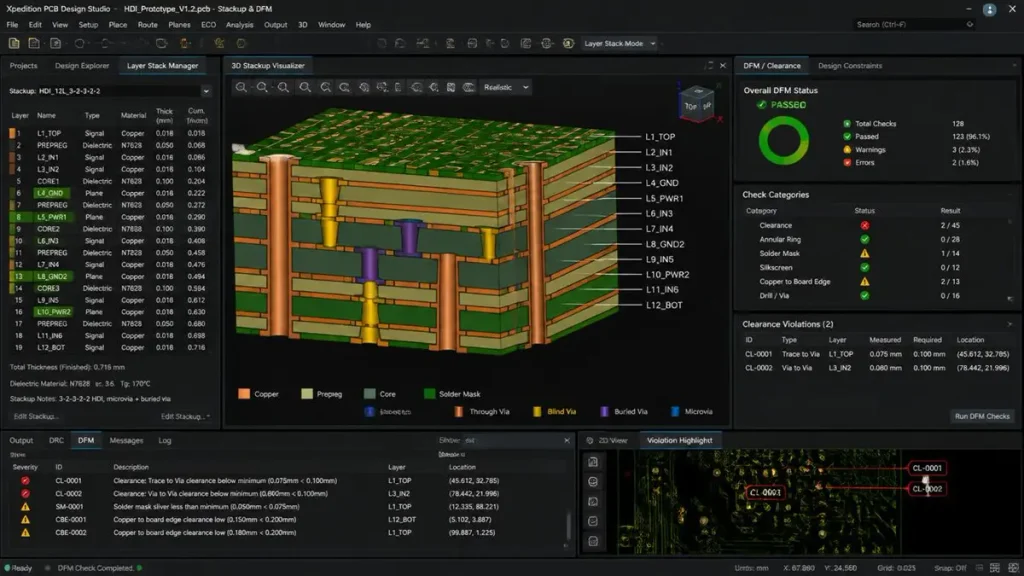
Computer screen displaying complex PCB CAD software with 3D stackup visualization and DFM clearance checks for an HDI PCB prototype project.
A prototype quotation based only on raw Gerber files may not reveal every manufacturability risk. Our DFM review covers:
- Minimum trace and space
- Laser‑drilled microvia diameter
- Capture‑pad and target‑pad dimensions
- Via‑to‑copper clearance
- Via‑in‑pad filling and capping requirements
- Stacked‑microvia geometry
- BGA fanout feasibility
- Layer‑to‑layer registration tolerance
- Copper thickness
- Solder‑mask clearance
- Component courtyard and assembly constraints
- Controlled‑impedance geometry
- Thermal relief and current‑carrying requirements
- Panelization and tooling layout
- Test‑point accessibility
- Depanelization risk
This review identifies potential redesign, yield, reliability, and cost issues before fabrication begins — reducing the risk of a failed or marginal prototype run.
HDI PCB Prototype Cost Factors
HDI prototype pricing is driven by several interacting factors rather than a single “per layer” rate:
- Layer count
- HDI structure and number of sequential‑lamination cycles
- Microvia diameter and density
- Stacked versus staggered microvia design
- Via‑in‑pad filling and copper capping
- Board size and panel utilization
- Material type and availability
- Copper thickness
- Surface finish
- Impedance‑control requirements
- Number of prototype pieces
- Testing and inspection requirements
- Expedited production requests
- Engineering or tooling requirements
- Shipping destination and customs requirements
Cost‑reduction checklist for buyers:
- Confirm the actual electrical need for each HDI layer before finalizing the stackup.
- Avoid unnecessarily small vias and trace/space where design margin allows.
- Use standard materials where performance requirements permit.
- Optimize panel utilization across your prototype quantity.
- Separate must‑have requirements from preferred requirements before requesting a quote.
- Confirm whether testing is required for every board or only for qualification samples.
HDI PCB Prototype Lead Time
Lead time is a range determined by several variables rather than a single fixed number:
| Stage | Key Variables |
|---|---|
| Engineering review | File completeness and design complexity |
| Material preparation | Material type and availability |
| Fabrication | HDI structure and layer count |
| Testing and inspection | Required test coverage |
| Shipping | Destination and carrier selection |
We provide a confirmed lead‑time estimate after reviewing your design files rather than a generic advertised turnaround, since HDI lead time depends heavily on stackup complexity and material lead times. We do not advertise blanket “24‑hour HDI prototype” claims — actual turnaround is confirmed per project based on the factors above.
Quality Control and Reliability Testing
We distinguish between routine production inspection and qualification‑level reliability testing, and confirm with each customer which level of testing applies to their prototype order:
| Test | What It Verifies | Routine or Optional |
|---|---|---|
| AOI | Circuit pattern integrity | Routine |
| Automated electrical test | Net continuity and isolation | Routine |
| Flying‑probe test | Continuity for low‑volume/prototype panels | Routine for prototypes |
| Impedance testing | Controlled‑impedance net compliance | Available on request |
| Microsection analysis | Via structure, plating thickness, lamination quality | Available on request |
| Plating‑thickness inspection | Copper and finish thickness compliance | Available on request |
| Solderability testing | Surface‑finish assembly readiness | Available on request |
| Thermal‑stress testing | Interconnect reliability under thermal cycling | Available on request |
| Via‑chain testing | Blind/buried via reliability | Available on request |
| Dimensional inspection | Board outline and hole‑position accuracy | Routine |
For each test performed, we can provide a corresponding inspection report, and sample retention can be arranged where required for your quality records.
Prototype‑to‑Production Transfer
Many HDI prototype orders never make it to production without re‑engineering, because the original process window was never documented in a transferable form. We control this transition through:
- Approved stackup documentation retained for the project record
- Material traceability from prototype through production
- Frozen Gerber files and fabrication notes at the point of prototype approval
- Formal revision control for any post‑approval design changes
- Golden sample retention for reference during production ramp‑up
- Documented process‑window parameters from the qualified prototype run
- First‑article inspection at the start of production
- Engineering‑change control for any subsequent modifications
- Repeat‑order review to confirm continued process capability
- Yield and defect tracking across the production transition
- Production panelization confirmation aligned with the original design intent
The practical result: the stackup and process that passed your prototype qualification is the same one used for production, rather than a re‑engineered version discovered to differ once volumes begin.
Applications for HDI PCB Prototypes
- AI servers and GPU computing — high pin‑count BGA fanout and low‑loss materials for signal integrity.
- High‑speed networking and switches — controlled impedance and tight layer registration.
- Mobile and wearable electronics — miniaturization and fine‑pitch component support.
- Medical devices — high reliability and regulatory traceability.
- Automotive electronics — thermal cycling resistance and qualified material systems.
- Aerospace and defense — vibration resistance and high‑reliability workmanship standards.
- Industrial controls — durability under variable operating conditions.
- Cameras and imaging systems — compact form factor with dense routing.
- Compact IoT products — space‑constrained layouts requiring HDI density.
- Advanced consumer electronics — combined miniaturization and cost sensitivity.
How to Request an HDI PCB Prototype Quote
For an accurate quotation, please provide:
- Gerber, ODB++, IPC‑2581, or native CAD files
- Board outline and dimensions
- Layer count
- Finished board thickness
- Copper thickness
- Material requirement
- HDI structure
- Microvia and buried‑via requirements
- Surface finish
- Solder‑mask and legend colors
- Impedance requirements
- Quantity
- Required testing
- Target delivery date
- Shipping destination
- Applicable quality standard
- Assembly requirements, if applicable
Two quotation paths are available:
- Quick Quote — for customers with complete manufacturing files ready for review.
- Engineering Consultation — for customers with incomplete or early‑stage designs who need guidance before file finalization.
Request Your HDI PCB Prototype Quote from Shenzhen Hongda Circuit Technology → pcb@pcbkr.com
Visit www.pcbkr.com to upload your files or schedule an engineering consultation.
Frequently Asked Questions
What is an HDI PCB prototype?
An HDI PCB prototype is a small production run of a high‑density interconnect circuit board used to verify electrical performance, mechanical fit, assembly behavior, and manufacturing feasibility before volume production. HDI boards commonly use laser‑drilled microvias, fine lines and spaces, sequential lamination, blind or buried vias, and compact BGA fanout structures.
What does HDI mean in PCB manufacturing?
HDI means high‑density interconnect. In PCB manufacturing, it refers to board structures that use fine‑line circuitry, microvias, blind vias, buried vias, and sequential lamination to create more interconnections in less space than conventional through‑hole multilayer construction.
When should I use an HDI PCB instead of a standard multilayer PCB?
Use HDI when component pitch, routing density, board size, or electrical requirements cannot be met efficiently with conventional through vias. HDI is especially useful for fine‑pitch BGAs, compact products, high‑layer‑count designs, and applications requiring shorter interconnect paths or more routing layers in a smaller footprint.
What HDI structures can Shenzhen Hongda Circuit Technology produce?
We support structures such as 1+N+1, 2+N+2, staggered microvias, stacked microvias, any‑layer HDI, buried vias, and via‑in‑pad, subject to confirmation against your specific design geometry, material selection, and target reliability during DFM review.
Can you manufacture HDI prototypes with 0.4 mm pitch BGA components?
0.4 mm pitch BGA fanout is feasible depending on pad size, escape pattern, microvia diameter, trace‑and‑space requirements, stackup, solder‑mask design, and assembly rules. We complete a DFM review before confirming manufacturability and price for fine‑pitch designs.
Are stacked microvias reliable for prototypes?
Stacked microvias can be reliable when the design, dielectric thickness, copper plating, filling, capping, and thermal‑stress controls are properly qualified. They are generally more demanding than staggered microvias, so we recommend requesting cross‑section evidence and a clearly documented fabrication process before committing to a stacked‑microvia design.
Do HDI PCBs require sequential lamination?
Most HDI PCBs require one or more sequential‑lamination cycles because microvias are formed in build‑up dielectric layers after the core structure is laminated. The number of cycles depends on the HDI structure, via depth, layer count, and whether the design uses stacked or staggered microvias.
Can HDI prototypes support controlled impedance?
Yes. HDI prototypes can support controlled impedance when we receive accurate stackup information and control dielectric thickness, copper thickness, trace geometry, etching, registration, and testing. Please specify target single‑ended or differential impedance values and identify critical nets in your fabrication documentation.
How much does an HDI PCB prototype cost?
HDI prototype cost depends on layer count, board size, HDI structure, material, microvia density, sequential lamination, via filling, copper thickness, surface finish, testing, quantity, and delivery speed. A reliable quote requires complete design files and manufacturing specifications rather than only a board outline or schematic.
Why are HDI PCB prototypes more expensive than standard PCB prototypes?
HDI prototypes cost more because they often require laser drilling, sequential lamination, finer registration control, microvia metallization, additional inspection, specialized materials, and more complex process control. Low quantities also spread engineering, tooling, setup, and testing costs across fewer boards.
How long does an HDI PCB prototype take?
Lead time depends on design complexity, material availability, HDI structure, lamination cycles, testing, quantity, and shipping. We provide a lead‑time commitment after reviewing your files, distinguishing engineering time, fabrication time, inspection time, and transit time.
About Shenzhen Hongda Circuit Technology Co., Ltd.
Shenzhen Hongda Circuit Technology Co., Ltd. manufactures HDI PCB prototypes and production boards for customers who need both technical depth and a transparent procurement process — from engineering review and quotation through fabrication, testing, delivery, and production ramp‑up.
Website: www.pcbkr.com
Request an engineering review or quote: Upload your design files at www.pcbkr.com or contact our engineering team directly. Email:pcb@pcbkr.com
Specific capability figures, lead‑time ranges, and pricing referenced in this page should be confirmed with our engineering team for your exact design, as actual capability depends on board construction, material selection, copper thickness, and design geometry.
About Author
David Chen https://www.linkedin.com/in/pcbcoming
David Chen boasts an extensive professional background in PCBA manufacturing, PCBA testing, and PCBA optimization, with specialized expertise in high-precision PCBA fault analysis and rigorous PCBA reliability testing. The author has worked with high-layer-count server PCB fabrication, ultra-low-loss backplane stackups, and thermo-mechanical reliability optimization for AI infrastructure projects involving 112G and 224G PAM4 architectures. Skilled in complex circuit design and cutting-edge advanced PCB manufacturing processes, he delivers solutions that elevate product durability and performance across industrial applications. His technical articles focusing on PCBA manufacturing workflows and testing methodologies are widely cited by industry peers, research institutions, and technical platforms, solidifying his reputation as a recognized technical authority in the global circuit board manufacturing sector.