
Common DFM Issues in PCB Design: 12 Errors to Check Before Manufacturing
Introduction
Common DFM issues in PCB design include insufficient trace width and spacing, inadequate annular rings, incorrect drill clearances, solder mask defects, unsuitable via structures, stackup inconsistencies, component footprint errors, and incomplete manufacturing files. These problems can cause fabrication failures, assembly defects, additional engineering costs, and production delays. A structured design for manufacturability (DFM) review helps engineers and buyers identify risks before releasing a PCB for manufacturing.
A PCB layout that passes electrical design rule checking (DRC) is not necessarily ready for production. The design must also meet the capabilities of the selected manufacturer, the requirements of the intended assembly process, and the product’s electrical and mechanical specifications.
For OEM procurement teams, resolving these issues before placing an order can reduce unnecessary engineering iterations and improve the transition from prototype to volume production.
This guide explains the most common PCB DFM problems, their manufacturing consequences, practical corrective actions, and the questions buyers should ask before selecting a PCB manufacturing supplier.
What Are the Most Common DFM Issues in PCB Design?
The most common DFM issues affect PCB geometry, drilling, solder mask definition, via construction, layer stackup, component assembly, and manufacturing documentation.
The following table summarizes 12 issues that should be reviewed before releasing a PCB design for fabrication or assembly.
| DFM issue | Potential manufacturing consequence | Recommended corrective action |
|---|---|---|
| Insufficient trace width or spacing | Open circuits, shorts, or reduced manufacturing yield | Verify geometry against copper thickness and process capabilities |
| Insufficient annular ring | Pad breakout or reduced connection reliability | Review drill size, pad diameter, and registration tolerances |
| Incorrect drill-to-copper clearance | Isolation failures or manufacturing defects | Check plated and non-plated hole clearances |
| Incorrect solder mask design | Exposed copper, unintended coverage, or soldering problems | Verify mask expansion and solder mask dam requirements |
| Unsuitable via structure | Plating, filling, or assembly reliability problems | Confirm via type, aspect ratio, and filling requirements |
| Insufficient copper-to-edge clearance | Exposed copper or routing-related defects | Check board-edge and depanelization constraints |
| Incorrect stackup or impedance design | Electrical performance outside specification | Validate materials, layer geometry, and impedance targets |
| Uneven copper distribution | Warpage or dimensional instability | Review copper balance and lamination requirements |
| Incorrect component footprints | Soldering defects or assembly rework | Verify land patterns against component specifications |
| Inadequate component spacing | Placement, inspection, or rework difficulties | Check assembly clearances and component orientation |
| Incomplete manufacturing files | Quotation delays and production misunderstandings | Cross-check fabrication and assembly deliverables |
| Poor panelization or test access | Assembly handling or testing difficulties | Review production tooling, breakaway features, and test access |
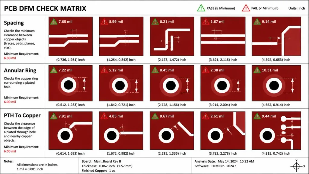
PCB DFM Check Matrix: Spacing, Annular Ring, and PTH to Copper Analysis
These issues do not automatically cause defects in every design. Their actual impact depends on board construction, manufacturing tolerances, component selection, assembly methods, and the capabilities of the chosen supplier.
Why Can a PCB Pass DRC but Still Fail a Manufacturer’s DFM Review?
Design rule checking verifies that a PCB layout complies with a defined set of design constraints. A DFM review evaluates whether those constraints and the complete manufacturing data are suitable for the intended production process.
The distinction matters because CAD rules may not reflect the actual process limits of the selected PCB manufacturer.
For example, a design tool may accept a particular trace width and spacing because the engineer has configured those values as permitted. However, the manufacturer may need additional process margin for the specified copper thickness, etching process, layer registration, and finished board requirements.
Other issues may not be detected by ordinary DRC checks, including:
- Conflicts between Gerber files and the fabrication drawing.
- Missing or inconsistent stackup information.
- Incomplete impedance requirements.
- Unsuitable panelization or routing features.
- Component footprints that create assembly difficulties.
- Manufacturing notes that conflict with the supplied production data.
A comprehensive review should therefore combine CAD-based rule checking with manufacturing engineering review.
For projects requiring coordinated PCB fabrication and PCBA assembly preparation, buyers can also review the PCB and PCBA NPI engineering services offered by PCBKR.
Which Trace Width, Spacing, and Annular Ring Errors Cause PCB Fabrication Problems?
Trace geometry and drilled-hole design are among the first areas to check because they directly affect electrical isolation, copper connectivity, and manufacturing tolerances.
How Do Trace Width and Spacing Violations Affect PCB Yield?
Trace width determines the cross-sectional area available to carry current, while spacing determines the electrical clearance between conductive features.
If traces are too narrow for the specified current and copper thickness, excessive temperature rise may become a concern. If spacing is insufficient, manufacturing variation or contamination can contribute to short circuits or inadequate electrical isolation.
The appropriate values depend on several factors:
- Finished copper thickness.
- Current requirements and acceptable temperature rise.
- PCB material and layer construction.
- Etching capability and dimensional tolerances.
- Operating voltage and required electrical clearance.
- The manufacturer’s qualified process window.
For high-density designs, engineers should not simply reduce trace width and spacing until the layout fits. They should verify that the proposed geometry is manufacturable and electrically appropriate.
Recommended action: Confirm the manufacturer’s capability for the intended copper thickness and minimum geometry before finalizing the layout. For high-current designs, separately verify conductor current capacity and thermal performance.
Why Does Insufficient Annular Ring Create Reliability Risks?
An annular ring is the copper remaining around a drilled hole or via after drilling and fabrication tolerances are considered.
If the pad is too small relative to the finished hole and potential drill displacement, the resulting annular ring may become inadequate. In severe cases, the drill can break out of the pad, compromising the intended connection.
Engineers should consider:
- The finished hole diameter.
- The drill diameter required before plating.
- Pad diameter and shape.
- Layer-to-layer registration tolerances.
- The relevant manufacturing class and supplier requirements.
A common mistake is to design the pad using only the nominal drill diameter without accounting for the complete manufacturing process.
Recommended action: Confirm hole and pad dimensions with the manufacturer, particularly for fine-pitch components, dense via fields, and high-layer-count boards.
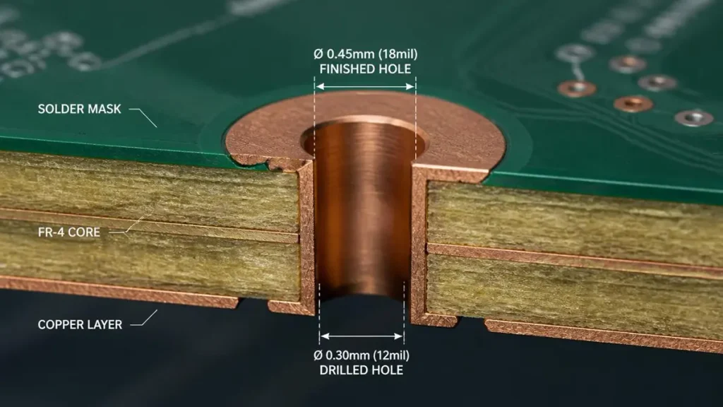
PCB PTH and Annular Ring Cross-Section Structure Analysis
How Should Engineers Check Drill-to-Copper and Copper-to-Edge Clearance?
Drill-to-copper clearance prevents unwanted proximity between holes and nearby conductive features. Copper-to-edge clearance helps prevent copper exposure and other problems associated with board routing or depanelization.
The required clearances depend on whether a hole is plated or non-plated, the board construction, the routing process, and the manufacturer’s tolerances.
Designers should also distinguish between copper clearance to the finished board edge and clearance to the routed or milled profile.
Recommended action: Review drill files, copper layers, and the fabrication drawing together. Do not rely on a single clearance rule without considering the actual hole type and finished geometry.
Which Solder Mask, Silkscreen, and Via Design Mistakes Should Be Fixed Before Fabrication?
Solder mask, silkscreen, and via construction affect both bare-board manufacturability and downstream assembly quality.
How Do Solder Mask Slivers and Incorrect Mask Expansion Cause Problems?
Solder mask openings must align with the intended exposed copper features. Incorrect expansion may partially cover pads or expose more copper than intended.
When solder mask dams between adjacent pads become too narrow for the selected process, they may not be reproduced reliably. Depending on the design and assembly process, this can contribute to soldering difficulties or reduced insulation between features.
Before releasing the design, engineers should verify:
- Solder mask expansion around component pads.
- Minimum solder mask dam width supported by the supplier.
- Mask registration tolerances.
- Openings for exposed copper and test points.
- The intended finish and assembly process.
Recommended action: Ask the manufacturer to review fine-pitch solder mask features against its qualified process capability rather than assuming that every CAD-defined dam can be reproduced.
Why Should Silkscreen Text Stay Clear of Pads and Exposed Copper?
Silkscreen identifies components, polarity, connectors, test points, and assembly orientation. Text placed over pads or exposed copper may be clipped or removed during fabrication, making identification more difficult.
Poorly placed reference designators can also complicate assembly inspection, repair, and troubleshooting.
Recommended action: Keep essential markings readable and positioned away from solderable surfaces. Verify that polarity marks, connector labels, and revision identifiers remain visible on the finished board.
When Do Via-in-Pad, Via Filling, and Aspect Ratio Become DFM Risks?
Via-in-pad structures can support dense layouts, especially under fine-pitch BGA and other compact components. However, their suitability depends on the via construction and assembly requirements.
Unfilled vias in solderable pads can allow solder to drain into the hole during reflow. Depending on the geometry and process, this can affect solder joint formation.
Engineers should confirm:
- Whether vias are located inside solderable component pads.
- Whether filling and capping are required.
- The specified via filling and surface finishing process.
- The drilled-hole diameter and board thickness.
- The manufacturer’s qualified drilling and plating limits.
Via aspect ratio, commonly expressed as board thickness divided by drilled-hole diameter, is an important factor in plated through-hole manufacturing. The acceptable limit varies with the manufacturer’s process and the specified hole construction.
Recommended action: Specify the required via structure explicitly. Do not assume that via filling, copper capping, or other specialized processes are included unless they are confirmed in the manufacturing requirements and quotation.
How Can Stackup, Copper Balance, and Impedance Errors Increase PCB Manufacturing Cost?
Stackup and material decisions influence manufacturability, electrical performance, and cost. Problems in these areas may require engineering changes even when the PCB layout appears geometrically correct.
What Happens When the Specified Stackup Does Not Match the Impedance Target?
Controlled impedance depends on the conductor geometry, dielectric properties, reference-plane arrangement, and surrounding structure.
If the specified stackup differs from the construction used to calculate impedance, the finished transmission line may not meet the required electrical target.
Potential causes include:
- Incorrect dielectric thickness assumptions.
- Different copper thickness from the design model.
- An unsuitable dielectric constant assumption.
- Incorrect reference-plane placement.
- Inconsistent impedance requirements between design files and fabrication notes.
These issues are particularly important for high-speed digital interfaces, RF circuits, and other applications where transmission-line performance affects product operation.
Recommended action: Provide the manufacturer with the required impedance values, relevant layer assignments, stackup information, and applicable tolerances. Have the proposed construction reviewed before production.
Where required, discuss impedance calculation, test coupon design, and impedance test reporting with the supplier.
Why Can Uneven Copper Distribution Cause Warpage?
Uneven copper distribution across layers can contribute to dimensional instability and warpage, depending on the stackup, material properties, lamination conditions, and overall board construction.
The risk can become more significant in multilayer boards with asymmetric structures or substantial differences in copper coverage between layers.
Engineers should consider:
- Copper distribution across the board and individual layers.
- Stackup symmetry where appropriate.
- Core and prepreg selection.
- Board thickness and aspect ratio.
- Assembly temperature exposure and mechanical requirements.
Recommended action: Review copper balance and stackup construction with the manufacturer. Copper balancing features should be introduced only when electrically and mechanically appropriate for the design.
How Do Material and Process Choices Affect Manufacturability?
Material selection affects more than electrical performance. It also influences drilling, lamination, dimensional stability, thermal behavior, and fabrication cost.
For example, a high-speed PCB may require a low-loss laminate, controlled dielectric geometry, and specific copper characteristics. An HDI design may require specialized laser drilling, microvia formation, or sequential lamination.
These requirements can affect:
- Available manufacturing processes.
- Material sourcing and lead time.
- Fabrication complexity.
- Inspection and testing requirements.
- Prototype-to-volume-production consistency.
Recommended action: Confirm material availability and process compatibility before committing to the design. For complex projects, request a manufacturing review before finalizing the stackup and design rules.
Which PCB Assembly DFM Issues Are Often Missed During Bare-Board Design?
A bare PCB can satisfy fabrication requirements while still creating difficulties during SMT assembly, inspection, or testing. Assembly design should therefore be reviewed separately from bare-board manufacturability.
How Do Incorrect Footprints and Pad Geometry Cause SMT Defects?
Component footprints determine the relationship between the component terminals, PCB pads, and solder paste deposits.
Incorrect pad geometry can contribute to insufficient solder joints, bridging, component misalignment, or inconsistent soldering results.
Potential causes include:
- Footprints that do not match the component manufacturer’s recommended land pattern.
- Incorrect pad dimensions or spacing.
- Inappropriate solder paste aperture assumptions.
- Incorrect orientation or polarity information.
- Thermal pad designs that do not account for the assembly process.
Recommended action: Verify critical footprints against the component datasheet and review the design with the intended assembly process in mind.
For fine-pitch packages, BGA devices, and thermal-pad components, the PCB footprint and solder paste design should be considered together.
How Can Component Spacing and Orientation Affect SMT Assembly?
Component spacing affects placement access, soldering, optical inspection, and rework. Components positioned too close to board edges or other components may be difficult to handle or inspect.
Orientation also matters for polarized devices, connectors, and components whose placement affects signal routing or thermal performance.
Recommended action: Review component clearances, placement orientation, fiducial requirements, and assembly access with the PCBA supplier before production.
Why Should Thermal Pads and Test Points Be Reviewed Before Assembly?
Thermal pads help transfer heat from components into the PCB. Their design may include multiple vias, copper areas, and solder paste patterns. An unsuitable combination can affect solder distribution or thermal performance.
Test points are equally important when the product requires in-circuit testing, flying-probe testing, or other electrical verification.
If test points are inaccessible, too small, or obstructed by components, the intended test procedure may require modification.
Recommended action: Confirm thermal requirements and test access early. Specify the intended test method and discuss any fixture or probe constraints before releasing the assembly design.
How Do Incomplete Gerber Files and Manufacturing Notes Delay PCB Orders?
Manufacturing files define the geometry, construction, and special requirements of a PCB. Incomplete or inconsistent documentation can prevent the supplier from preparing an accurate quotation or proceeding with production.
Which PCB Fabrication Files Should Buyers Submit?
The exact deliverables depend on the board and supplier, but a typical PCB fabrication package includes:
- Gerber files or ODB++ manufacturing data.
- Excellon drill files with plated and non-plated hole information.
- A fabrication drawing with dimensions and tolerances.
- Layer stackup information.
- Material and copper thickness specifications.
- Surface finish requirements.
- Controlled impedance requirements, where applicable.
- Special processing instructions and inspection requirements.
For PCBA projects, the package may also need:
- Bill of materials (BOM).
- Pick-and-place or centroid file.
- Assembly drawings.
- Component polarity and orientation information.
- Solder paste data where required.
- Programming, functional testing, or traceability requirements where applicable.
Not every project requires every file. The goal is to provide a complete and consistent production package for the agreed scope.
How Should Buyers Prevent Revision Conflicts Between Manufacturing Files?
Revision conflicts occur when different files describe different versions of the same product.
For example, the Gerber data may reflect a revised component location while the assembly drawing still refers to the previous revision. A drill file may also fail to match the supplied copper layers.
Such inconsistencies can result in engineering clarification, incorrect fabrication, or assembly rework.
Recommended action:
- Assign a clear revision identifier to the production package.
- Confirm that fabrication and assembly files refer to the same revision.
- Remove obsolete files from the release package.
- Document approved changes and deviations.
- Require confirmation before any manufacturing change that affects product requirements.
What Should a Manufacturer’s DFM Report Include?
A useful DFM report should identify problems and help the design team decide what to do next.
It should ideally include:
- The affected layer, feature, component, or file.
- The applicable design rule or manufacturing requirement.
- The potential manufacturing or assembly consequence.
- A recommended corrective action.
- The severity and production implications of the issue.
- Whether customer approval is required for a proposed deviation.
- The final status and revision of the reviewed design.
A report that simply lists errors without explaining their impact may not provide enough information for engineering or procurement teams to prioritize corrections.
How Can PCB DFM Problems Increase Quotation Costs and Lead Times?
DFM issues affect manufacturing costs through several mechanisms. Some require design clarification, while others may require special processes, additional inspection, or a design revision.
| DFM problem | Potential cost or schedule impact | Preventive action |
|---|---|---|
| Geometry outside standard process capability | Special processing or redesign | Confirm capabilities before layout completion |
| Unresolved stackup and impedance requirements | Engineering iterations or additional verification | Validate construction before production |
| Inconsistent manufacturing files | Quotation delays and repeated clarification | Release one controlled file revision |
| Assembly footprint problems | Trial builds, rework, or process adjustments | Perform a separate DFA review |
| Inaccessible test points | Test fixture changes or reduced test access | Confirm the test strategy before layout release |
| Unresolved critical DFM findings | Production holds or redesign | Close or formally approve critical issues |
The financial impact depends on the product, order quantity, complexity, and manufacturing process. A small design correction before fabrication may be straightforward, while a problem discovered after tooling, fabrication, or assembly can require substantially more work.
Buyers should therefore evaluate not only the initial PCB unit price but also the completeness of the engineering review, the clarity of the manufacturing quotation, and the handling of design changes.
What Should Buyers Check Before Choosing a PCB Manufacturer for DFM Review?
A PCB manufacturer should be able to explain how it evaluates manufacturability, communicates risks, and manages changes before production.
Procurement teams should ask the following questions.
1. Can you review Gerber or ODB++ data before production?
Confirm which data formats are accepted and whether the review includes geometry, drilling, stackup, and fabrication notes.
2. Do you review both PCB fabrication DFM and assembly DFA?
For PCBA projects, confirm whether component footprints, spacing, soldering requirements, and test access are reviewed as part of the agreed scope.
3. Can you validate the proposed stackup against controlled-impedance requirements?
Ask how the stackup is evaluated and what information is required to confirm the intended electrical performance.
4. Will you provide a documented DFM report?
A written report helps engineering teams prioritize corrections and gives procurement teams a record of unresolved issues.
5. How are deviations and engineering changes approved?
Clarify whether production can proceed with an unresolved issue and who must authorize any deviation from the approved design.
6. What inspection and electrical test reports are available?
The required evidence depends on the product. Discuss relevant inspection, electrical testing, impedance verification, and documentation requirements before placing the order.
7. Can the proposed process support both prototype and volume production?
A process that works for a small prototype order may not be the most economical or repeatable choice for volume manufacturing. Ask the supplier to identify any changes that may be needed as production volume increases.
For buyers evaluating a manufacturing partner, the PCB manufacturer page provides a starting point for reviewing PCB fabrication services. Projects requiring low-volume assembly can also explore low-volume PCB assembly manufacturing.
What Is the Final PCB DFM Checklist Before Sending Files to a Manufacturer?
Before releasing a design, engineering and procurement teams should verify that the PCB is not only electrically complete but also ready for fabrication, assembly, and testing.
Use this checklist during the final production-readiness review.
PCB Fabrication
- Trace width and spacing match the intended fabrication process.
- Annular rings and drill-to-copper clearances are verified.
- Copper-to-edge clearance and routing constraints are checked.
- Solder mask openings and silkscreen placement are reviewed.
- Via structures, filling requirements, and aspect ratios are confirmed.
- Stackup, materials, copper thickness, and impedance requirements are consistent.
- Copper distribution and potential warpage risks are reviewed.
PCB Assembly and Testing
- Component footprints match the intended parts.
- Component spacing and orientation are suitable for assembly.
- Thermal pads and solder paste requirements are reviewed.
- Test points are accessible for the intended test method.
- Panelization and depanelization requirements are confirmed.
Manufacturing Documentation
- Gerber or ODB++ data matches the drill files and fabrication drawing.
- BOM and pick-and-place files match the approved assembly revision.
- Material, finish, thickness, tolerance, and special process requirements are documented.
- Critical DFM findings are closed or formally approved.
- The production package has a clear revision identifier.
A checklist helps standardize the process, but it does not replace a manufacturer-specific engineering review. The final design should be evaluated against the actual process capabilities and product requirements.
Frequently Asked Questions About Common DFM Issues in PCB Design
What are the most common DFM issues in PCB design?
The most common issues include insufficient trace width and spacing, inadequate annular rings, incorrect drill clearances, solder mask errors, unsuitable via structures, stackup inconsistencies, incorrect component footprints, and incomplete manufacturing files. Their severity depends on the board construction and the manufacturer’s process capabilities.
Why does my PCB pass DRC but fail DFM review?
DRC checks compliance with configured CAD rules, while DFM review evaluates whether the complete design can be manufactured reliably using the intended process. A PCB may pass DRC but still have insufficient process margin, inconsistent manufacturing files, unsuitable stackup information, or assembly-related problems.
What should be included in a PCB DFM checklist?
A PCB DFM checklist should cover trace geometry, drilling, annular rings, solder mask, vias, copper distribution, stackup, impedance, component footprints, assembly clearances, test access, and manufacturing file consistency. The checklist should be adapted to the board’s specifications and the selected supplier.
What are the minimum trace width and spacing requirements for PCB manufacturing?
There is no single minimum trace width and spacing that applies to every PCB. The acceptable values depend on copper thickness, fabrication technology, layer construction, electrical requirements, and the manufacturer’s qualified capabilities. Confirm the limits with the supplier before finalizing the layout.
Can DFM issues increase PCB manufacturing costs?
Yes. DFM issues can require special processing, additional engineering reviews, revised manufacturing files, new tooling, extra testing, or redesign. Identifying these issues before production usually provides more flexibility to correct them before they affect manufacturing or assembly.
When should a PCB design undergo DFM review?
A PCB design should undergo preliminary DFM review during layout planning, a more complete review after the design is finalized, and a final manufacturing-data check before production release. Complex or high-density designs may benefit from earlier consultation with the manufacturer.
What files does a PCB manufacturer need for DFM analysis?
Typical files include Gerber or ODB++ data, drill files, a fabrication drawing, stackup information, and material and finish specifications. For assembly, the supplier may also require a BOM, pick-and-place file, assembly drawings, and additional testing or programming requirements.
Does PCB DFM review cover SMT assembly problems?
Not necessarily. Bare-board DFM focuses on PCB fabrication, while DFA evaluates assembly-related factors such as footprints, component spacing, soldering, polarity, and rework access. PCB and PCBA projects should coordinate these reviews before production.
How can I choose a PCB manufacturer that provides reliable DFM support?
Look for a supplier that can explain its manufacturing capabilities, review production files, document DFM findings, clarify process limitations, and manage approved design changes. For PCBA, also verify the scope of assembly review, inspection, and testing.
Should a PCB prototype undergo the same DFM review as mass production?
Both prototypes and mass-production boards require DFM review, but the emphasis may differ. Prototype reviews often focus on design feasibility and rapid correction, while volume-production reviews should also consider process repeatability, panelization, inspection coverage, assembly efficiency, and cost.
Need a PCB DFM Review Before Production?
Resolving manufacturability issues before fabrication can help reduce avoidable engineering iterations, clarify supplier requirements, and prepare a PCB design for production.
Shenzhen Hongda Circuit Technology Co., Ltd. supports PCB and PCBA manufacturing projects that require engineering coordination between design requirements and manufacturing preparation.
To discuss a project, prepare the relevant Gerber or ODB++ files, drill data, stackup requirements, and fabrication notes. For assembly projects, include the BOM, pick-and-place file, and assembly drawings.
About Author
David Chen LinkedIn Profile
David Chen is a Senior RF/PCB Process Engineer at Shenzhen Hongda Circuit Technology Co., Ltd., with over 12 years of experience in high-frequency PCB fabrication, impedance-controlled stack-up design, and Rogers/PTFE laminate processing. He also boasts an extensive professional background in PCBA manufacturing, PCBA testing, and PCBA optimization, with specialized expertise in high-precision PCBA fault analysis and rigorous PCBA reliability testing. The author has worked with high-layer-count server PCB fabrication, ultra-low-loss backplane stackups, and thermo-mechanical reliability optimization for AI infrastructure projects involving 112G and 224G PAM4 architectures. Skilled in complex circuit design and cutting-edge advanced PCB manufacturing processes, he delivers solutions that elevate product durability and performance across industrial applications. His technical articles focusing on PCBA manufacturing workflows and testing methodologies are widely cited by industry peers and technical platforms, and have gained attention and recognition from industry colleagues.