How Do You Choose an Oscilloscope PCB Manufacturer for OEM Production?
Choosing an oscilloscope PCB manufacturer requires more than comparing board prices. OEM buyers need a supplier that can manufacture the specified stack-up, control critical dimensions, support PCB assembly, and provide inspection evidence appropriate to the design. Shenzhen Hongda Circuit Technology Co., Ltd. supports PCB manufacturing and PCBA requirements, helping electronics manufacturers move from prototype orders toward repeatable production with clear engineering requirements and quality controls.
What Should an Oscilloscope PCB Manufacturer Provide to OEM Buyers?
An oscilloscope PCB manufacturer should be able to review the customer’s fabrication data, confirm manufacturing requirements, identify potential production risks, and explain which inspection and assembly services are available. For OEM procurement teams, the objective is to establish whether the supplier can meet the documented requirements—not simply whether it can manufacture a multilayer board.
Oscilloscope designs vary considerably. A general-purpose instrument may combine an analog front end, input protection, signal conditioning, an analog-to-digital converter (ADC), digital processing, memory, and power-management circuits. Higher-bandwidth instruments may impose tighter requirements on interconnects, impedance, dielectric properties, and signal integrity.
Shenzhen Hongda Circuit Technology Co., Ltd. provides PCB manufacturing and PCBA services for customers who need to evaluate fabrication and assembly requirements together. The appropriate manufacturing route depends on the customer’s design files, materials, specifications, order quantity, and testing requirements.
For a meaningful quotation, buyers should distinguish among three deliverables:
- Bare PCB fabrication: Manufacturing the board to the approved fabrication data and specifications.
- PCBA: Assembling components onto the fabricated PCB according to the BOM, placement data, assembly drawings, and approved process requirements.
- System-level verification: Confirming the completed oscilloscope’s measurement performance against its design requirements. This may require customer-owned test procedures, dedicated fixtures, calibrated instruments, and system-level engineering beyond standard board fabrication.
These deliverables should be defined separately in the RFQ to avoid gaps in responsibility or unexpected costs.
Which Oscilloscope PCB Design Requirements Affect Manufacturing?
The manufacturing requirements depend on the signal chain, operating bandwidth, component selection, board geometry, and the OEM’s acceptance criteria. A supplier should review the actual design rather than assume that every oscilloscope requires the same layer count, material, or advanced fabrication process.
How Should the Analog Front End Be Manufactured?
The analog front end may contain attenuators, input protection, amplifiers, filters, switches, and ADC-driving circuitry. These circuits can be sensitive to parasitic capacitance, leakage, contamination, trace geometry, component placement, and coupling from nearby switching or digital circuits.
A practical engineering review should check:
- Whether the specified trace widths, spacing, clearances, and pad geometries are manufacturable.
- Whether the board stack-up and copper arrangement match the approved design.
- Whether sensitive input nodes and high-impedance circuits require particular cleanliness or handling controls.
- Whether the component packages and footprints match the assembly data.
- Whether fabrication changes could affect critical dimensions or electrical behavior.
A PCB manufacturer can identify fabrication and assembly risks, but it should not claim that manufacturing alone will eliminate analog noise. Noise performance also depends on the circuit topology, component characteristics, grounding and return paths, power integrity, layout, shielding, and measurement setup.
Why Do ADC and Digital Interfaces Need Careful PCB Review?

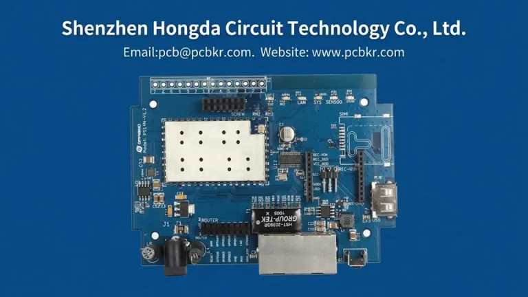
Oscilloscope PCB ADC and digital interface layout illustrating signal integrity and controlled impedance considerations.
ADC and digital interfaces can require careful control of signal integrity, impedance, stack-up configuration, and interconnect geometry, depending on the oscilloscope’s bandwidth and circuit design. These requirements should be evaluated against the actual electrical specifications rather than assuming every oscilloscope PCB needs the same high-speed design features. For designs with demanding signal-integrity requirements, our high-speed PCB manufacturing guide provides additional information about high-speed PCB fabrication considerations.
ADC interfaces, sampling clocks, memory buses, and digital-processing circuits can introduce fast signal transitions and switching currents. Poorly controlled interconnects or return paths may contribute to ringing, coupling, or electromagnetic interference.
Where the design requires it, the supplier should confirm controlled-impedance specifications, stack-up information, copper geometry, dielectric construction, and the relevant inspection or measurement requirements before production.
Controlled impedance should not be specified simply because a board is used in an oscilloscope. It should be based on the interface requirements, signal edge rates, routing geometry, target impedance, and the customer’s design rules.
Does Every Oscilloscope PCB Need High-Frequency Materials or Ultra-Fine Lines?
No. Material selection and line geometry should follow the electrical design and manufacturing constraints.
Standard FR-4 may be appropriate for many sections of an instrument. Specialized high-frequency or low-loss materials may be justified for particular high-speed or RF signal paths, depending on loss, dielectric properties, frequency, and design margin.
Likewise, ultra-fine line-and-space processing, microvias, and advanced substrate technologies should be selected only when the layout, density, or electrical requirements call for them. Using an advanced process where it adds no meaningful benefit can increase cost and complexity without improving the instrument’s performance.
For procurement, the important question is whether the manufacturer can produce the specified construction consistently and document the relevant acceptance criteria.
How Can Advanced PCB Manufacturing Equipment Support Oscilloscope PCB Production?
Equipment matters when its capabilities correspond to a real design requirement. Shenzhen Hongda Circuit Technology Co., Ltd. has manufacturing equipment and inspection capabilities that can support demanding PCB fabrication requirements. The specific process used for an oscilloscope PCB should be selected according to the approved design rather than applying every advanced process to every order.
How Does LDI Support Pattern Accuracy?
Laser direct imaging (LDI) supports accurate transfer of circuit patterns onto the production panel. Shenzhen Hongda Circuit Technology Co., Ltd. uses SCREEN Ledia LDI equipment, with an 8 µm target and a stated ±10 µm capability.
These figures describe the imaging capability context; they are not a guarantee that every finished trace, space, or board feature will achieve the same tolerance. Final geometry also depends on the full process, including imaging conditions, copper processing, etching compensation, materials, and design rules.
For oscilloscope PCB buyers, LDI is relevant when fine features, dense routing, or tighter pattern requirements need to be reviewed against the actual fabrication specification.
When Are Laser-Drilled Microvias Relevant?
Via dimensions affect routing density, layer transitions, and the manufacturability of multilayer boards. Shenzhen Hongda Circuit Technology Co., Ltd. uses Mitsubishi UV/CO₂ laser equipment with a stated 75 µm ±5 µm capability and picosecond laser equipment capable of 50 µm processing.
These capabilities may be relevant when a design genuinely requires small laser-drilled features or dense interconnections. They do not mean that every oscilloscope PCB needs microvias or that every 50–75 µm feature is automatically appropriate for the design. Via structure, target pad, copper plating, stack-up, reliability requirements, and the applicable process window must be evaluated together.
For many oscilloscope boards, conventional multilayer construction may be sufficient. The correct choice is the simplest manufacturing structure that meets the documented electrical, mechanical, and reliability requirements.
How Does Lamination Control Affect Multilayer Boards?
Layer registration, dielectric thickness, resin flow, and bonding quality influence the construction of multilayer PCBs. Shenzhen Hongda Circuit Technology Co., Ltd. uses LAUFFER lamination equipment with stated pressure capabilities of 80, 150, and 200 psi and a vacuum capability below 50 mbar.
These are equipment operating capabilities, not universal process settings for every board. The appropriate lamination recipe depends on the material system, copper distribution, finished thickness, stack-up, and approved manufacturing process.
For OEM procurement, the practical question is whether the supplier can manufacture the specified stack-up and maintain the required construction tolerances—not whether the highest available pressure is always used.
When Does mSAP Fine-Line Processing Matter?
Modified semi-additive processing (mSAP) can support fine-line circuit structures where conventional subtractive processing does not meet the required geometry or density. Shenzhen Hongda Circuit Technology Co., Ltd. has stated an 8/8 µm mSAP capability.
This should be treated as a design-dependent capability rather than a standard requirement for oscilloscope PCBs. Many instrument boards do not require 8/8 µm traces and spaces. mSAP becomes relevant only when the actual routing density, pad geometry, or other design constraints justify it and the selected stack-up and materials are compatible with the process.
The RFQ should therefore specify the required line-and-space geometry instead of assuming that an advanced process is inherently better.
What Quality Inspection Should OEM Buyers Request?
Inspection should be defined according to the board’s construction, risk level, and customer acceptance criteria. A reliable procurement process identifies what is checked, how the results are recorded, and which party is responsible for each test.
Shenzhen Hongda Circuit Technology Co., Ltd. has stated inspection capabilities that include automated optical inspection (AOI), X-ray inspection, four-wire Kelvin flying-probe testing, and vector network analyzer (VNA) measurement up to 70 GHz.
Each method serves a different purpose:
| Inspection or measurement method | What it can help evaluate | What buyers should confirm |
|---|---|---|
| AOI | Visible pattern defects and selected manufacturing features | Inspection coverage, acceptance criteria, and records |
| X-ray inspection | Internal features or concealed solder joints where applicable | Whether the package or board structure requires X-ray inspection |
| Four-wire Kelvin flying-probe test | Electrical continuity and resistance-related measurements using an appropriate setup | Test coverage, limits, and whether the required test program is available |
| VNA measurement | Frequency-dependent electrical behavior of suitable test structures or interconnects | Frequency range, calibration, fixture, test structure, and acceptance limits |
A VNA capable of measuring up to 70 GHz does not mean every oscilloscope PCB is tested to 70 GHz. High-frequency measurements require an appropriate test objective, suitable fixtures or test structures, calibration, and agreed acceptance criteria.
Similarly, bare-board electrical testing does not verify the completed oscilloscope’s bandwidth, noise floor, ADC effective number of bits (ENOB), or measurement accuracy. Those are system-level performance characteristics and must be verified under an agreed test plan.
Before placing an order, buyers should specify which records they require, such as electrical test results, dimensional inspection, impedance reports where applicable, assembly inspection records, material documentation, or batch traceability information.
How Can PCB Manufacturing Help Address Noise and Signal-Integrity Problems?
Noise problems often emerge when analog, power, and digital circuits interact. Public engineering discussions on Reddit illustrate the kinds of issues designers may encounter: noisy ADC readings, uncertainty about input protection and filtering, and questions about analog-to-digital grounding and return paths.
For example, engineers discussing a 20 MSPS oscilloscope analog front end have raised questions about input attenuation, protection, filtering, and the interface to the ADC. Other mixed-signal design discussions describe concerns about digital switching noise entering sensitive analog measurement circuits.
These discussions are useful as examples of engineering pain points, but they are not controlled test results or proof that one PCB fabrication method will solve the problem.
For OEM buyers, they suggest several practical manufacturing checks.
Scenario 1: ADC Readings Contain Unexpected Noise
If a prototype produces noisy readings, the root cause may involve the analog front end, power supply, grounding, clock coupling, component behavior, PCB layout, assembly defects, or the measurement setup.
The manufacturer can help review fabrication data, confirm stack-up and construction, check for manufacturing defects, and inspect assembly quality where those services are included. The design team may still need to investigate circuit stability, power integrity, component selection, and system-level behavior.
A useful RFQ should identify critical analog regions and specify any special manufacturing, cleaning, inspection, or test requirements.
Scenario 2: The Input Protection Circuit Changes the Measured Waveform
Attenuators, protection components, filters, and buffers can affect bandwidth, loading, and waveform shape. The PCB supplier should manufacture the approved footprints, spacing, and routing geometry accurately and flag manufacturing concerns that are within its engineering review scope.
The OEM remains responsible for confirming that the selected circuit topology and component values meet the intended input range and performance requirements. Any layout or fabrication change near a sensitive input should be reviewed and approved before implementation.
Scenario 3: Digital Switching Interferes with Sensitive Measurements
An oscilloscope may combine low-level analog signals with fast digital interfaces and switching power circuits. Return paths, layer arrangement, decoupling placement, and circuit partitioning are primarily design concerns, but the manufacturing supplier must build the approved construction consistently.
Buyers should confirm that the stack-up, copper thickness, impedance requirements, and any special layout notes are included in the manufacturing package. A supplier should not independently change critical copper geometry or layer construction without authorization.
Scenario 4: The Prototype Works, but the Production Batch Is Inconsistent
A prototype-to-production transition can expose problems with revision control, material substitutions, process variation, assembly documentation, or incomplete acceptance criteria.
OEM buyers should establish a controlled release package, define approval requirements for engineering changes, and agree on inspection records and nonconformance handling. These controls are often more valuable to long-term procurement than an unsupported promise that every batch will be identical.
What Affects Oscilloscope PCB Manufacturing Cost and Lead Time?
There is no single price or lead time that applies to all oscilloscope PCBs. The quotation depends on the actual design, order quantity, materials, process route, assembly scope, component availability, and delivery requirements.
| Cost or schedule factor | Why it matters to the quotation |
|---|---|
| Layer count and finished thickness | Affect materials, lamination cycles, drilling, and process complexity |
| Copper weight and finished copper requirements | Affect processing conditions and feature manufacturability |
| Controlled impedance | May require stack-up review, process controls, test structures, or measurement |
| Specialized materials | Can change material cost, processing conditions, and availability |
| Fine lines, microvias, or advanced structures | May require specialized process steps and additional engineering review |
| PCB quantity and panel utilization | Affect material utilization, setup cost, and unit pricing |
| PCBA scope | Depends on the BOM, package types, placement complexity, and soldering requirements |
| Component sourcing | Depends on availability, approved alternatives, lead times, and procurement responsibility |
| Inspection and functional testing | Depend on coverage, fixtures, test programs, and acceptance requirements |
| Required delivery date | May affect scheduling, material choices, and expedited-production costs |
For an accurate quote, buyers should distinguish the requested delivery date from the manufacturing lead time and include component procurement, assembly, testing, and shipping in the schedule discussion.
Can the Same Supplier Support Prototypes and Production?
Potentially, but buyers should confirm the actual production scope and qualification requirements. A prototype order should establish whether the fabrication data is complete, the selected materials and stack-up are feasible, and the agreed acceptance criteria can be met.
Before moving to production, the OEM should review the first-article results where applicable, approve the final revision, confirm component sourcing arrangements, and document any required process or inspection controls.
A supplier’s ability to manufacture a prototype does not automatically establish that it can meet every production-volume, reliability, regulatory, or system-level testing requirement. These requirements should be reviewed explicitly before the purchase order is released.
How Should Buyers Compare Oscilloscope PCB Manufacturers?
A useful supplier comparison evaluates engineering fit, manufacturing evidence, commercial terms, and communication—not price alone.
| Evaluation point | Questions to ask the supplier |
|---|---|
| Relevant manufacturing capability | Can the supplier meet the specified layer count, thickness, copper, material, and feature geometry? |
| Engineering review | Will the supplier identify incomplete files or manufacturing conflicts before production? |
| Quality inspection | Which checks are included, and what reports are available? |
| PCBA scope | Are components supplied by the customer or the manufacturer? Are substitutions subject to approval? |
| Testing responsibility | Which tests are included in the quote, and which require customer-provided fixtures or procedures? |
| Revision control | How are revised Gerber, BOM, placement, and assembly files released and controlled? |
| Delivery terms | Does the schedule include fabrication, sourcing, assembly, inspection, and shipping? |
| Issue resolution | How are nonconformities reported, investigated, and approved for disposition? |
Shenzhen Hongda Circuit Technology Co., Ltd. encourages buyers to provide the actual technical requirements so that the manufacturing route, inspection scope, and quotation can be evaluated against the intended application.
The most suitable supplier is the one that can demonstrate a fit with the documented requirements and communicate the limits of its responsibility clearly.
What Information Should You Include in an Oscilloscope PCB RFQ?
A complete request for quotation reduces avoidable engineering questions and helps suppliers return more comparable offers.
For Bare PCB Fabrication
Include:
- Gerber or ODB++ manufacturing data and drill files.
- Stack-up drawing, layer count, finished board thickness, and thickness tolerance.
- Copper weight requirements and any special finished-copper specifications.
- Material requirements and any controlled-impedance targets.
- Surface finish, solder mask, silkscreen, and relevant dimensional tolerances.
- Board quantity, prototype or production status, and target delivery date.
- Required inspection reports, electrical test requirements, and acceptance criteria.
For PCBA
Also provide:
- BOM with manufacturer part numbers and approved alternatives, if any.
- Centroid or pick-and-place file.
- Assembly drawings and polarity or orientation notes.
- SMT and through-hole requirements.
- Component-sourcing preference: turnkey, consigned, or mixed supply.
- Required AOI, X-ray, ICT, functional testing, or other agreed checks.
- Test procedures, fixtures, and acceptance limits where testing is requested.
Do not assume that a supplier can quote system-level oscilloscope testing from PCB files alone. If the requirement includes bandwidth, noise, calibration, or acquisition-performance verification, provide the test specification and clarify who will supply the test setup and approve the results.
Request an Oscilloscope PCB Quote from Shenzhen Hongda Circuit Technology Co., Ltd. Submit your available manufacturing files, target quantity, required delivery date, and inspection or assembly requirements. The engineering and sales review can then determine the appropriate fabrication route and clarify any missing information before quotation. Email: sales@pcbkr.com
Frequently Asked Questions About Oscilloscope PCB Manufacturing
How Do I Choose a Reliable Oscilloscope PCB Manufacturer?
Compare the supplier’s ability to meet your actual board specifications, its engineering-review process, available inspection evidence, PCBA capabilities, revision control, and delivery terms. Ask which tests are included and request relevant records rather than relying solely on general claims about quality.
How Much Does Custom Oscilloscope PCB Manufacturing Cost?
Cost depends on layer count, dimensions, materials, copper requirements, impedance control, special structures, quantity, assembly complexity, component sourcing, testing, and delivery requirements. Submit complete fabrication data and a defined scope to receive a meaningful quotation.
Does an Oscilloscope PCB Require Controlled Impedance?
Not every board requires the same impedance controls. The need depends on the interfaces, signal edge rates, routing, target impedance, and design requirements. When controlled impedance is specified, provide the stack-up and target values and clarify whether test structures or impedance reports are required.
What Testing Should Be Included When Ordering Oscilloscope PCBA?
The test plan may include bare-board electrical testing, AOI, X-ray for applicable packages, in-circuit testing, or functional testing. These methods are not interchangeable. If the requirement includes oscilloscope bandwidth, noise, calibration, or measurement accuracy, define a separate system-level verification plan and identify the responsible party.
Can One Supplier Support Both Oscilloscope PCB Prototypes and Mass Production?
A supplier may support both, but buyers should verify the actual capabilities, order quantities, process controls, material availability, and quality requirements. Before production release, approve the final revision, agree on inspection and change-control requirements, and establish how nonconforming products will be handled.
What Files Are Needed for an Oscilloscope PCB Quote?
For bare PCB fabrication, provide Gerber or ODB++ data, drill files, stack-up, materials, thickness, copper, finish, quantity, and delivery requirements. For PCBA, add the BOM, placement data, assembly drawings, component-sourcing instructions, and requested testing scope.
Can Advanced Laser Processing Improve an Oscilloscope PCB?
Laser processing can support designs that require small drilled features or dense interconnections. It is not automatically necessary for every oscilloscope PCB. The required via dimensions, pad geometry, stack-up, materials, and reliability requirements should determine whether laser-drilled structures are appropriate.
Does a PCB Manufacturer Guarantee the Oscilloscope’s Measurement Accuracy?
Bare-board fabrication and PCBA inspection alone cannot establish complete instrument accuracy. Measurement performance depends on the circuit design, components, layout, firmware, calibration, test conditions, and other system factors. The parties should define the system-level test procedure and acceptance criteria separately.
Request a Quote for Your Oscilloscope PCB Project
Shenzhen Hongda Circuit Technology Co., Ltd. works with customers evaluating PCB fabrication and PCBA requirements for electronic products. To help assess your oscilloscope PCB project, provide the available design files, construction requirements, quantity, delivery target, and any special inspection or testing needs.
A clear RFQ makes it easier to review manufacturability, confirm the requested production scope, identify open engineering questions, and prepare a quotation aligned with your requirements.
About Author
David Chen LinkedIn Profile
David Chen is a Senior RF/PCB Process Engineer at Shenzhen Hongda Circuit Technology Co., Ltd., with over 12 years of experience in high-frequency PCB fabrication, impedance-controlled stack-up design, and Rogers/PTFE laminate processing. He also boasts an extensive professional background in PCBA manufacturing, PCBA testing, and PCBA optimization, with specialized expertise in high-precision PCBA fault analysis and rigorous PCBA reliability testing. The author has worked with high-layer-count server PCB fabrication, ultra-low-loss backplane stackups, and thermo-mechanical reliability optimization for AI infrastructure projects involving 112G and 224G PAM4 architectures. Skilled in complex circuit design and cutting-edge advanced PCB manufacturing processes, he delivers solutions that elevate product durability and performance across industrial applications. His technical articles focusing on PCBA manufacturing workflows and testing methodologies are widely cited by industry peers and technical platforms, and have gained attention and recognition from industry colleagues.