How Can OEMs Source Computing Accelerator Card PCBA Manufacturing?
Computing Accelerator Card PCBA manufacturing combines bare PCB fabrication, electronic component sourcing and board-level assembly for AI computing, GPU computing and high-performance computing applications. PCBKR provides integrated PCB manufacturing, full or partial BOM sourcing, SMT, THT and BGA assembly, including supported 0.4 mm pitch BGA packages, followed by AOI, X-ray inspection and electrical testing according to project requirements.
What Is Included in Computing Accelerator Card PCBA Manufacturing?
A computing accelerator card PCBA is an assembled electronic board designed to perform specialized computing tasks in AI, GPU processing, high-performance computing (HPC) and data-processing systems.
Unlike a bare PCB, a completed PCBA includes the electronic components mounted and soldered onto the fabricated circuit board. Manufacturing therefore requires coordination between PCB fabrication, component procurement, assembly processes and inspection.
PCBKR provides an integrated manufacturing route covering the following stages:
| Manufacturing stage | Service scope |
|---|---|
| PCB fabrication | Multilayer, HDI and high-speed PCB manufacturing |
| Component sourcing | Full BOM sourcing, partial sourcing or customer-supplied components |
| SMT assembly | Surface-mount component placement and soldering |
| THT assembly | Through-hole component and connector assembly |
| BGA assembly | BGA placement and soldering, including supported 0.4 mm pitch packages |
| PCBA inspection | AOI and X-ray inspection |
| Electrical testing | Testing based on agreed project requirements |
| Final delivery | Bare PCBs, procured components and completed PCBAs |
This integrated approach allows OEM purchasing teams to coordinate PCB production, component sourcing and assembly through one manufacturing supplier.
Delivery scope: PCBKR supplies the bare PCB, procured components and assembled PCBA according to the agreed order. Heatsink installation, cooling-system integration, chassis assembly and complete card mechanical integration are not included in the standard service scope.
Which Computing Accelerator Card Applications Can PCBKR Support?
Computing accelerator cards are used in systems that require dedicated processing resources, high-speed data communication and substantial power delivery.
PCBKR evaluates manufacturing projects according to the customer’s PCB design, component list, assembly files and production requirements.
Typical application categories include:
AI Accelerator Card PCBA
AI accelerator cards are designed for parallel computing workloads, including model training, inference and other AI processing tasks.
Their PCB assemblies may require high-density component placement, complex BGA packages, multilayer routing and carefully controlled power distribution.
GPU Computing Card PCBA
GPU computing cards combine high-performance processing devices with memory, power-management components and high-speed interfaces.
For these products, the manufacturing review should consider BGA package requirements, PCB stackup, component placement, solder-joint inspection and electrical testing.
HPC and Data Processing Accelerator Boards
High-performance computing and data-processing equipment may use dedicated accelerator boards to support computationally intensive workloads.
Depending on the design, these assemblies can involve multilayer or HDI PCBs, high-density component placement and specialized power and signal structures.
Custom Computing Accelerator Boards
OEMs may also require custom accelerator boards for proprietary computing platforms, embedded systems or specialized processing equipment.
PCBKR reviews each project based on its actual manufacturing files rather than assuming that all accelerator cards share the same PCB construction or assembly requirements.
How Does Turnkey Component Sourcing Work for Accelerator Card PCBA?
Component sourcing is a major part of PCBA procurement. A supplier must coordinate the BOM, manufacturer part numbers, package information, component quantities and availability before assembly can proceed.
PCBKR supports three component-sourcing arrangements.
What Is the Difference Between Full and Partial BOM Sourcing?
| Sourcing arrangement | Customer responsibility | PCBKR responsibility |
|---|---|---|
| Full BOM sourcing | Provides the approved BOM and project requirements | Sources the required components and performs PCB assembly |
| Partial BOM sourcing | Supplies selected components | Sources the remaining components and performs assembly |
| Customer-supplied components | Supplies the required components | Receives the components and performs assembly |
These arrangements allow OEMs to choose a sourcing model based on their existing supplier relationships, component availability and purchasing policies.
How Should Component Shortages and Long Lead Times Be Managed?
Some accelerator card projects contain specialized processors, memory devices, power-management ICs and high-speed interface components.
The availability of these parts can affect the production schedule even when the bare PCB is ready.
Before procurement, buyers should review:
- Manufacturer part numbers and approved manufacturers.
- Required quantities and component package information.
- Component availability and estimated procurement lead times.
- Parts with long lead times or limited availability.
- Customer requirements for approved sourcing channels.
- Any special handling or storage requirements.
Component availability should be confirmed during quotation and purchasing rather than assumed from an earlier BOM review.
How Should Buyers Control Component Substitutions?
An alternative component should not be treated as automatically interchangeable with the original part.
Before approving a substitution, the buyer and engineering team should review:
- Electrical characteristics and operating ratings.
- Package dimensions and footprint compatibility.
- Pin configuration and functional compatibility.
- Thermal and reliability requirements.
- Compatibility with the existing PCB design and assembly process.
Any proposed substitution should receive customer approval before it is incorporated into the production BOM.
Why Are BOM Revisions and Component Quantities Important?
An outdated BOM can result in incorrect component procurement, missing parts or assembly errors.
For a more controlled procurement process, buyers should provide a clearly identified BOM revision and confirm the required quantity per board, total production quantity and any approved alternatives.
Component overage and unused-component handling should also be agreed before production, particularly for customer-supplied or specially procured components.
What Makes 0.4 mm Pitch BGA Assembly Challenging?
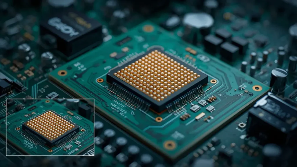
Computing Accelerator Card PCBA with 0.4 mm pitch BGA assembly and precision solder joints
Fine-pitch BGA assembly requires careful coordination between PCB pad design, solder paste application, component placement, reflow conditions and inspection.
PCBKR supports BGA assembly, including 0.4 mm pitch packages. For accelerator card projects, this capability is particularly relevant when the design uses high-pin-count processors, memory devices or other fine-pitch packages.
How Do BGA Pad and Via Designs Affect Assembly Quality?
BGA assembly quality begins with the PCB design.
Important design considerations include:
- BGA pad dimensions and spacing.
- Solder mask-defined or non-solder-mask-defined pad structures.
- Via-in-Pad design.
- Via filling and capping requirements.
- Solder mask registration.
- PCB surface finish.
- Local copper distribution and board flatness.
Via-in-Pad structures can help support dense BGA routing, but the via construction must be appropriate for the soldering process.
Unfilled or inadequately controlled vias can create solder-wicking risks. OEMs should therefore identify via filling, capping and other special requirements in the fabrication data and stackup documentation.
How Do PCB Warpage and Component Coplanarity Affect BGA Soldering?
BGA solder joints are hidden beneath the package after assembly.
Differences in PCB flatness, package warpage and component coplanarity can affect the formation of reliable solder connections.
The engineering review should consider:
- PCB thickness and overall dimensions.
- Material selection and thermal characteristics.
- Copper distribution across the board.
- Package dimensions and warpage information.
- Component placement and reflow requirements.
These factors should be evaluated together rather than treating BGA assembly as an isolated SMT operation.
How Should Solder Paste and Reflow Requirements Be Reviewed?
For fine-pitch BGA packages, solder paste volume and thermal conditions require appropriate process control.
Relevant manufacturing considerations include:
- Stencil aperture design.
- Solder paste selection.
- Paste deposition consistency.
- Component package specifications.
- Reflow profile requirements.
- PCB and component thermal limitations.
The actual process window should be established according to the package, PCB construction, soldering materials and assembly conditions.
How Does X-ray Inspection Identify Hidden BGA Defects?
Unlike conventional optical inspection, X-ray inspection can examine solder joints hidden underneath BGA packages.
It is useful for evaluating issues such as:
- Solder bridging.
- Insufficient solder or abnormal solder distribution.
- Voiding.
- Open or potentially defective solder connections.
X-ray images should be evaluated against appropriate inspection criteria and the requirements agreed for the project. An X-ray image alone does not establish the complete electrical or functional performance of an assembled accelerator card.
Which PCB Materials and Manufacturing Specifications Matter for Accelerator Cards?
Accelerator card performance depends on more than component selection. PCB construction, material properties, copper distribution and interconnection structures also influence signal integrity, power delivery and assembly manufacturability.
The appropriate specifications depend on the actual interface requirements, package design, board dimensions and operating environment.
What PCB Stackup and Material Requirements Should Buyers Review?
The stackup determines how signal, ground and power layers are arranged within the PCB.
Before production, OEM engineering teams should review:
| Specification | Engineering consideration |
|---|---|
| Layer count | Routing density and signal/power layer allocation |
| Board thickness | Mechanical requirements and connector compatibility |
| Base material | FR-4, High-Tg or low-loss material according to application |
| Copper weight | Signal routing and power distribution requirements |
| Dielectric thickness | Impedance and insulation requirements |
| Surface finish | Component solderability and assembly compatibility |
| Via structure | Through-hole, blind, buried and microvia requirements |
For high-speed designs, material selection should consider dielectric constant (Dk), dissipation factor (Df), copper roughness and the required operating frequency.
PCBKR’s HDI PCB manufacturing capability is relevant to designs requiring dense interconnections and fine-pitch component breakout.
How Do Controlled Impedance and Signal Integrity Affect High-Speed Boards?
High-speed accelerator cards may contain differential interfaces and high-speed connections between processors, memory and other electronic components.
Their PCB designs may require:
- Controlled differential impedance.
- Appropriate signal and reference-plane arrangements.
- Dielectric material selection.
- Controlled trace geometry.
- Via transition management.
- Backdrilling where required by the design.
- Insertion-loss and return-loss targets.
The stackup, trace geometry, material properties and via structures must be considered together.
PCBKR’s High-Speed PCB manufacturing capability provides further information about high-speed PCB requirements.
For projects requiring measurement of high-frequency electrical characteristics, PCBKR has VNA equipment capability up to 70 GHz. The applicable measurement method, test coupon, frequency range and acceptance limits should be agreed for each project. VNA measurement capability should not be confused with complete PCIe protocol or system-level compliance certification.
How Do Microvias and HDI Structures Affect BGA Breakout?
High-density BGA packages can require routing structures that are difficult to implement with conventional through-hole vias alone.
HDI manufacturing uses laser-drilled microvias and, where the design requires them, blind, buried, stacked or staggered via structures to support dense interconnections.
Relevant manufacturing considerations include:
- Microvia diameter and depth.
- Via aspect ratio.
- Via filling and copper plating.
- Layer registration.
- Sequential lamination.
- Pad and land dimensions.
- Microvia reliability under thermal and mechanical stress.
PCBKR uses Mitsubishi UV/CO₂ laser equipment and precision laser processing to support applicable HDI and microvia manufacturing requirements.
For further technical information, see the Microvia PCB manufacturing guide.
How Does Copper Thickness Affect Power Distribution?
Accelerator cards may contain power-management circuits and high-current power paths.
The PCB design must consider copper thickness, conductor width, power-plane configuration, via structures and connector requirements.
Important engineering checks include:
- Current requirements for each power path.
- Copper thickness and conductor geometry.
- Voltage drop and power distribution.
- Via current distribution.
- Temperature-rise limits.
- Copper balance and PCB warpage.
- Thermal requirements defined by the OEM.
Heavy copper construction may be appropriate for selected power-distribution areas, but copper weight should be determined by the actual electrical and thermal design.
See Heavy Copper PCB manufacturing for further information.
How Do PCBKR Manufacturing Equipment and Processes Support Accelerator Card PCB Production?
Advanced PCB manufacturing requires coordinated control of imaging, drilling, lamination and circuit formation. These processes become particularly important when accelerator card designs combine fine-pitch BGA packages, dense interconnections and high-speed signal requirements.
PCBKR’s manufacturing equipment supports several key process stages.
How Does LDI Imaging Support Fine-Line PCB Fabrication?
Laser Direct Imaging (LDI) transfers circuit patterns directly onto photosensitive material using digital exposure.
Compared with conventional film-based exposure, LDI can support precise pattern imaging and process compensation for demanding PCB constructions.
PCBKR uses SCREEN Ledia LDI equipment with an 8 µm target capability and ±10 µm process specification.
For accelerator card manufacturing, fine-line imaging is relevant to:
- Dense signal routing.
- Fine-pitch BGA breakout.
- High-density HDI structures.
- Fine-line mSAP circuit formation.
The achievable finished line width and spacing depend on the complete imaging, plating, etching, material and inspection process. The LDI equipment specification should not be interpreted as a guaranteed finished trace dimension on every board.
How Does Laser Drilling Support HDI and Microvia Fabrication?
Laser drilling enables the formation of small-diameter blind microvias used to connect selected PCB layers.
PCBKR’s relevant equipment includes:
| Equipment | Capability | Manufacturing application |
|---|---|---|
| Mitsubishi UV/CO₂ laser | 75 µm ±5 µm | Applicable HDI and microvia drilling processes |
| Picosecond laser | 50 µm | Precision laser processing for suitable structures |
Laser drilling is particularly important when the PCB design requires dense interconnections beneath fine-pitch BGA packages.
The final microvia structure must still be qualified according to the material, copper construction, drilling depth, plating process and reliability requirements.
How Does Lamination Affect Multilayer PCB Consistency?
Multilayer accelerator card PCBs may require several signal, ground and power layers bonded into a single structure.
Lamination quality affects layer bonding, registration, dielectric thickness and the mechanical stability of the finished board.
PCBKR uses LAUFFER lamination equipment with process pressure settings of 80, 150 and 200 psi and a vacuum level below 50 mbar.
These process parameters support controlled lamination for applicable PCB constructions. The actual pressure, temperature and cycle must be determined according to the laminate system, stackup and production process.
How Does mSAP Technology Support High-Density Accelerator Card Designs?
Modified Semi-Additive Process (mSAP) is used to manufacture fine-line circuits by building copper traces through a controlled plating process rather than relying solely on conventional subtractive etching.
As circuit density increases, mSAP can help support finer trace geometries and more compact routing structures.
PCBKR has an 8/8 µm mSAP capability established since Q3 2024.
For accelerator card applications, fine-line manufacturing can be relevant to:
- High-density BGA breakout.
- Dense signal routing.
- Advanced HDI structures.
- Compact multilayer interconnections.
mSAP should be selected according to the actual design requirements, production volume and cost target. It is not automatically required for every accelerator card.
For a deeper explanation of fine-line manufacturing, see the mSAP PCB Fine-Line HDI Manufacturing Guide.
How Does PCBKR Inspect and Test Completed Accelerator Card PCBAs?
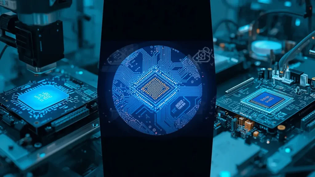
Computing Accelerator Card PCBA inspection with AOI, BGA X-ray and electrical testing
PCBA inspection should be defined according to component package types, board complexity and customer acceptance requirements.
PCBKR supports AOI inspection, X-ray inspection and electrical testing.
What Defects Can AOI Inspection Identify?
Automated Optical Inspection (AOI) uses optical imaging to examine visible assembly features.
Depending on the inspection program and component type, AOI can help identify:
- Missing components.
- Incorrect component placement.
- Polarity and orientation issues.
- Visible soldering defects.
- Component alignment problems.
AOI is useful for inspecting visible assembly features, but it cannot directly inspect solder joints hidden beneath BGA packages.
Why Is X-ray Inspection Important for BGA Components?
BGA solder joints are located underneath the component package and cannot be fully inspected through conventional optical imaging.
X-ray inspection provides a way to examine these hidden connections and identify solder-joint conditions that require further review.
For fine-pitch BGA packages, X-ray inspection is an important part of the agreed PCBA quality-control process.
What Does Electrical Testing Verify?
Electrical testing is used to verify specified electrical requirements of the assembled board.
The exact test scope should be defined before production. Depending on the project, the customer may specify continuity, short-circuit or other electrical checks.
Test coverage, test fixtures, test points and acceptance criteria should be reviewed against the design and available test data.
AOI, X-ray and electrical testing serve different purposes. None should be represented as a substitute for complete system-level functional validation, burn-in or PCIe protocol compliance testing.
How Should Buyers Define PCBA Inspection and Acceptance Criteria?
Before placing an order, OEMs should specify:
- Required AOI inspection coverage.
- BGA X-ray inspection requirements.
- Electrical test items and limits.
- Applicable workmanship and acceptance criteria.
- Required inspection records.
- Any customer-specific quality documentation.
Agreeing on these requirements before production helps avoid different interpretations of what constitutes an acceptable finished PCBA.
What Causes Computing Accelerator Card PCBA Production Delays?
A PCB assembly schedule depends on more than the time required for SMT placement and soldering.
For complex accelerator card projects, several upstream factors can affect the final delivery date.
Component Availability and Long Lead Times
Specialized processors, memory devices and power-management components may have different procurement lead times.
A delayed critical component can hold up the entire assembly even when the PCB has already been fabricated.
Buyers should identify long-lead-time parts early and confirm the sourcing plan before approving the production schedule.
Incomplete or Inconsistent Manufacturing Files
Missing drill files, outdated BOM revisions, incomplete Pick-and-Place data or unclear assembly drawings can require additional engineering clarification.
Gerber, BOM and placement data should refer to the same approved design revision.
BGA Design and PCB DFM Issues
BGA pad structures, via-in-pad requirements, solder mask design and PCB flatness can affect assembly feasibility.
Identifying these issues during the engineering review is preferable to discovering them after PCB fabrication or component procurement.
Delayed Engineering Approvals and Component Substitutions
Production may be delayed if an alternative component requires approval or if the customer has not confirmed an unresolved design or inspection requirement.
A clear approval process helps keep procurement and manufacturing aligned.
How Can Buyers Reduce Avoidable Production Delays?
OEM purchasing teams can reduce preventable delays by preparing a complete manufacturing package, confirming the BOM revision, identifying long-lead-time components and agreeing on inspection requirements before production.
What Files Should OEMs Prepare for a Computing Accelerator Card PCBA RFQ?
A complete RFQ package allows the manufacturer to evaluate PCB fabrication, component procurement, assembly complexity and testing requirements more accurately.
| Required file or information | Purpose |
|---|---|
| Gerber or ODB++ | PCB fabrication data |
| NC drill files | Hole and via manufacturing |
| PCB stackup | Layer, material and copper specifications |
| BOM | Component identification and sourcing |
| Pick-and-Place file | Component coordinates and orientation |
| Assembly drawings | Component placement and special instructions |
| BGA package information | Pitch, package dimensions and assembly requirements |
| Test requirements | Electrical test scope and acceptance criteria |
| Production quantity | Prototype, small-batch or volume planning |
| Target delivery schedule | Procurement and manufacturing planning |
Before submission, buyers should check that:
- The BOM and Gerber files use the same design revision.
- Manufacturer part numbers and package information are complete.
- DNP components are clearly identified.
- Pick-and-Place coordinates and component orientations are correct.
- Special BGA and via-in-pad requirements are documented.
- Electrical testing and inspection requirements are clearly specified.
A complete and consistent data package helps the engineering team evaluate the project before procurement and production begin.
Can PCBKR Support Accelerator Card PCBA from Prototype to Mass Production?
PCBKR supports prototype, small-batch and mass-production requirements for PCB and PCBA projects.
The appropriate production arrangement depends on the design maturity, component availability, order quantity and inspection requirements.
OEMs can choose:
- Full BOM sourcing with PCB fabrication and assembly.
- Partial BOM sourcing with customer-provided components.
- Customer-supplied components with PCB assembly.
- Prototype and small-batch manufacturing.
- Production orders based on an approved manufacturing package.
For projects moving from prototype to volume production, buyers should confirm that the PCB revision, BOM, assembly process and inspection criteria are controlled before increasing order quantities.
Production lead time and pricing should be confirmed against the actual files, component availability and requested quantity.
Why Choose PCBKR for Computing Accelerator Card PCBA Manufacturing?
Choosing a PCBA supplier for a computing accelerator card requires more than checking whether the supplier offers SMT assembly.
The supplier must be able to coordinate PCB fabrication, component sourcing, fine-pitch assembly and inspection requirements.
PCBKR provides the following manufacturing capabilities:
Integrated PCB and PCBA Manufacturing
Bare PCB fabrication, component sourcing and PCBA assembly are coordinated within the agreed project scope.
Full, Partial and Customer-Supplied BOM Options
OEMs can select a sourcing arrangement that matches their procurement strategy.
0.4 mm Pitch BGA Assembly
PCBKR supports BGA assembly, including 0.4 mm pitch packages, for applicable accelerator card designs.
SMT and THT Assembly
Surface-mount and through-hole assembly support mixed component requirements.
AOI, X-ray and Electrical Testing
Inspection and testing are performed according to the agreed project requirements.
Advanced PCB Manufacturing Equipment
SCREEN Ledia LDI, Mitsubishi UV/CO₂ laser drilling, picosecond laser processing and LAUFFER lamination equipment support applicable fine-line, HDI and multilayer PCB manufacturing processes.
Flexible Production Arrangements
PCBKR supports prototype, small-batch and mass-production requirements, subject to project review and production planning.
The standard final delivery is the bare PCB, procured components and assembled PCBA. Mechanical integration and complete card assembly are outside the standard delivery scope.
How Can OEMs Request a Computing Accelerator Card PCBA Quote?
If you are sourcing a manufacturer for an AI accelerator card, GPU computing card or HPC accelerator board, PCBKR can review your PCB fabrication, component sourcing, assembly and testing requirements.
To support an engineering and purchasing review, please prepare:
- Gerber or ODB++ files.
- PCB stackup and fabrication specifications.
- BOM with manufacturer part numbers.
- Pick-and-Place data.
- Assembly drawings.
- BGA package and pitch information.
- Prototype or production quantity.
- Required inspection and electrical testing specifications.
Request a Computing Accelerator Card PCBA Quote
Contact PCBKR to discuss your project requirements and request a manufacturing quotation.
Company: Shenzhen Hongda Circuit Technology Co., Ltd.
Email: sales@pcbkr.com
Website: www.pcbkr.com
Frequently Asked Questions About Computing Accelerator Card PCBA
How Do I Choose a Computing Accelerator Card PCBA Manufacturer?
Evaluate whether the manufacturer can support the complete manufacturing scope required by your project, including multilayer or HDI PCB fabrication, component sourcing, SMT and THT assembly, BGA processing, inspection and electrical testing.
For fine-pitch designs, confirm the supplier’s BGA pitch capability and whether X-ray inspection is available. Also review its engineering response, manufacturing documentation requirements and ability to support your expected production quantities.
Can PCBKR Assemble 0.4 mm Pitch BGA Components?
Yes. PCBKR supports BGA assembly, including 0.4 mm pitch packages. The project review should include BGA package dimensions, PCB pad design, via-in-pad requirements, soldering conditions and X-ray inspection requirements.
Can a PCBA Manufacturer Source the Complete BOM?
Yes. PCBKR supports full BOM sourcing, partial component sourcing and customer-supplied components. Buyers should provide manufacturer part numbers, quantities and approved component specifications. Any proposed component substitution should be confirmed with the customer before production.
What Documents Should I Send to Get a Computing Accelerator Card PCBA Quote?
Prepare Gerber or ODB++ files, NC drill data, PCB stackup, BOM, Pick-and-Place file, assembly drawings and production quantities. Include BGA package information, electrical testing requirements and any special inspection criteria to help the manufacturer assess the project accurately.
Does Computing Accelerator Card PCBA Manufacturing Include Heatsink Installation and Complete Card Assembly?
Not in PCBKR’s standard delivery scope. PCBKR provides bare PCB fabrication, component sourcing and completed PCBA assembly. Heatsink installation, cooling-system integration, chassis assembly and complete card mechanical integration are not included in the standard service.
About Author
David Chen LinkedIn Profile
David Chen is a Senior RF/PCB Process Engineer at Shenzhen Hongda Circuit Technology Co., Ltd., with over 12 years of experience in high-frequency PCB fabrication, impedance-controlled stack-up design, and Rogers/PTFE laminate processing. He also boasts an extensive professional background in PCBA manufacturing, PCBA testing, and PCBA optimization, with specialized expertise in high-precision PCBA fault analysis and rigorous PCBA reliability testing. The author has worked with high-layer-count server PCB fabrication, ultra-low-loss backplane stackups, and thermo-mechanical reliability optimization for AI infrastructure projects involving 112G and 224G PAM4 architectures. Skilled in complex circuit design and cutting-edge advanced PCB manufacturing processes, he delivers solutions that elevate product durability and performance across industrial applications. His technical articles focusing on PCBA manufacturing workflows and testing methodologies are widely cited by industry peers and technical platforms, and have gained attention and recognition from industry colleagues.