How Do You Choose an Industrial IPC Motherboard PCB and PCBA Manufacturer?
An industrial IPC motherboard requires more than a conventional multilayer PCB. It must support reliable power distribution, high-speed interfaces, dense component routing, mechanical stability, and consistent assembly. Choosing the right PCB and PCBA manufacturer means verifying its actual fabrication processes, inspection equipment, electrical testing, and production controls.
For OEMs developing industrial computers, embedded platforms, automation controllers, machine-vision systems, and edge-computing hardware, the manufacturing supplier directly affects board quality, production yield, and long-term product consistency.
Shenzhen Hongda Circuit Technology Co., Ltd. (PCBKR) provides PCB fabrication and PCBA manufacturing support for complex electronic assemblies, connecting fine-line processing, HDI technology, controlled multilayer lamination, precision inspection, and electrical verification.
This guide explains the manufacturing requirements behind industrial IPC motherboards and how OEM buyers can evaluate a supplier using measurable process capabilities rather than general manufacturing claims.
1. What Is an Industrial IPC Motherboard and What Does Its PCB Require?
An industrial IPC motherboard is the central circuit board of an industrial computer or embedded computing platform. Its PCB must accommodate complex power distribution, high-speed communication, dense component placement, mechanical constraints, and the reliability requirements of its intended operating environment.
Industrial motherboards are used in applications such as:
- Industrial automation and machine control
- Machine vision and image-processing systems
- Industrial networking and communication equipment
- Edge computing and data acquisition
- Robotics and motion-control systems
- Transportation and energy-management equipment
- Embedded computing platforms
Although industrial and consumer motherboards may use similar processors, memory devices, and communication interfaces, their engineering priorities are not always the same.
An industrial motherboard may need to operate continuously in an enclosure with restricted airflow, withstand repeated thermal changes, support multiple external interfaces, and remain available for a longer product lifecycle. These requirements influence the PCB construction and manufacturing process.
Which PCB characteristics matter most?
| PCB characteristic | Manufacturing consideration | Potential engineering risk |
|---|---|---|
| Layer count | Multilayer stackup and layer registration | Routing congestion and registration errors |
| Controlled impedance | Dielectric thickness, copper geometry, and material selection | Signal reflection and transmission loss |
| Fine-line routing | Imaging and etching process control | Opens, shorts, and conductor-width variation |
| BGA escape routing | Pad design, via structure, and fine-line capability | Incomplete fan-out and routing congestion |
| Power distribution | Copper thickness, trace geometry, and via design | Excessive voltage drop and localized heating |
| Board flatness | Material selection, copper balance, and lamination | Assembly alignment and soldering problems |
| PCB inspection | AOI, X-ray, and electrical verification | Undetected fabrication or assembly defects |
A frequent engineering mistake is to evaluate a motherboard only by its layer count. A 12-layer board with poorly planned reference planes or an unsuitable stackup can perform worse than a properly engineered 8-layer design.
The correct manufacturing review starts with the actual design files, interface requirements, board dimensions, material specification, and acceptance criteria.
PCBKR manufacturing relevance: PCBKR’s published manufacturing platform includes LDI imaging, laser drilling, controlled lamination, HDI processing, AOI, X-ray inspection, flying-probe testing, and high-frequency electrical test capability. These processes are relevant to complex industrial motherboard PCB and PCBA projects, subject to design review and process qualification.
2. Which Industrial Motherboard Types and Form Factors Should OEM Buyers Consider?
OEM buyers should select the motherboard architecture according to computing requirements, available enclosure space, interface count, expansion needs, and maintenance strategy. ATX, Micro-ATX, Mini-ITX, single-board computers, and COM Express carrier boards have different mechanical and routing requirements.
Common industrial motherboard formats include:
| Form factor or architecture | Typical application | PCB manufacturing considerations |
|---|---|---|
| ATX | Industrial computers and expansion-intensive systems | Larger board area, multiple expansion slots, complex power distribution |
| Micro-ATX | Compact industrial PCs | Higher routing density within a smaller outline |
| Mini-ITX | Space-constrained embedded computers | Dense component placement and connector clearance |
| Single-board computer (SBC) | Dedicated embedded applications | High integration and limited routing space |
| COM Express carrier board | Modular embedded computing | High-density connectors, differential pairs, and application-specific I/O |
| Custom embedded motherboard | Dedicated OEM equipment | Non-standard dimensions, connector locations, mounting, and interface requirements |
Why does the architecture affect PCB manufacturing?
A large ATX board may provide more routing space, but it can introduce challenges involving board flatness, copper distribution, connector placement, and mechanical tolerances.
A compact Mini-ITX design has less routing space around processors, memory devices, and connectors. This can increase the need for fine-line routing, HDI structures, and carefully planned layer transitions.
COM Express requires a different approach. The compute module and carrier board are separate parts of a modular architecture. The carrier board provides application-specific interfaces and connections to the compute module. The PCB manufacturer is responsible for fabricating the carrier board according to the approved design, not automatically for designing the processor module or developing its BIOS.
What should OEM buyers provide?
For an accurate manufacturing review, provide:
- Board outline and mechanical drawing
- Mounting-hole positions
- Connector locations and part numbers
- Layer count and stackup requirements
- Minimum trace and spacing
- BGA pitch and package information
- Controlled-impedance requirements
- Board thickness and copper weight
Engineering recommendation: Do not select a PCB process solely from the motherboard form factor. A compact carrier board with high-speed connectors may require more demanding impedance and registration control than a larger industrial motherboard with relatively low-speed interfaces.
PCBKR evaluates manufacturing requirements against the supplied PCB data and agreed specifications. The applicable process route must be confirmed before production.
3. What PCB Materials and Stackup Designs Are Suitable for Industrial Motherboards?
Industrial motherboard materials and stackups should be selected according to signal speed, dielectric loss, layer count, copper thickness, thermal conditions, board dimensions, and manufacturing requirements. High-Tg FR-4 may suit many industrial designs, while selected high-speed applications may require lower-loss materials and tighter control of dielectric properties.
Material selection is not simply a question of choosing the highest-performance laminate. The material must match the electrical requirements and remain compatible with the fabrication process.
Which material properties should engineers evaluate?
| Material property | Why it matters | Engineering consideration |
|---|---|---|
| Dielectric constant (Dk) | Influences propagation delay and impedance | Use material-specific design data |
| Dissipation factor (Df) | Affects dielectric signal loss | Important for higher-frequency interfaces |
| Glass transition temperature (Tg) | Relates to resin-system thermal behavior | Match to assembly and operating conditions |
| Coefficient of thermal expansion (CTE) | Influences dimensional change with temperature | Important for multilayer registration and reliability |
| Copper roughness | Influences conductor loss at high frequencies | Consider HVLP copper where the design requires it |
| Moisture absorption | Can affect electrical and mechanical behavior | Evaluate material and environmental requirements |
| Copper weight | Affects current capacity and conductor geometry | Balance electrical, thermal, and routing requirements |
PCBKR’s published material information includes conventional and advanced laminate options such as S1000-2, I-Tera MT40, RO4350B, Rogers 4450F, and other specified material systems. The final selection must be confirmed against the actual design and material availability.
Why is stackup engineering a manufacturing issue?
A stackup is not merely a layer-order drawing. It defines the relationship between signal layers, reference planes, dielectric thicknesses, copper weights, and the overall board construction.
For example, a DDR interface routed over an uninterrupted reference plane behaves differently from a signal crossing a split plane or changing reference layers without an appropriate return path.
Similarly, a PCIe differential pair may meet the nominal trace-width requirement but still experience impedance discontinuities if the dielectric thickness, copper geometry, via transition, or reference-plane structure changes unexpectedly.
A practical stackup review should therefore examine:
- Signal-layer and reference-plane relationships.
- Dielectric thickness and material-specific Dk.
- Copper thickness and finished conductor geometry.
- Symmetry and copper balance.
- Via transitions and return-current paths.
- Lamination sequence and manufacturing registration.
How does PCBKR’s lamination equipment support multilayer production?
PCBKR’s published equipment information includes LAUFFER lamination systems with reported pressure settings of 80, 150, and 200 psi and vacuum capability below 50 mbar.
These values describe equipment and process capability references. They should not be interpreted as a universal recipe for every industrial motherboard.
The correct pressure and vacuum profile depends on the resin system, core and prepreg construction, copper distribution, board thickness, and lamination cycle.
A manufacturing problem that deserves particular attention is resin flow. Excessive or insufficient resin flow can affect dielectric thickness, void formation, layer bonding, and final board flatness.
For a high-layer-count motherboard, an inappropriate lamination recipe may cause dimensional changes that become visible only during subsequent drilling, registration, or assembly.
4. How Do Multilayer and HDI Technologies Affect Industrial Motherboard Manufacturing?
Multilayer and HDI technologies allow industrial motherboards to accommodate more signals, power connections, and high-density components within limited board space. Their manufacturing success depends on fine-line imaging, accurate drilling, microvia formation, layer registration, copper plating, and controlled sequential lamination.
As processors, memory devices, and high-speed connectors become more integrated, PCB routing space becomes increasingly constrained.
A motherboard may need to route DDR signals, PCIe lanes, Ethernet interfaces, USB connections, display signals, and multiple power domains through the same limited area.
When conventional through-hole routing cannot provide sufficient escape-routing space, HDI structures may become necessary.
Which HDI structures are relevant?
| HDI technology | Function | Manufacturing challenge |
|---|---|---|
| Blind via | Connects an outer layer to selected inner layers | Via depth and registration |
| Buried via | Connects internal layers | Sequential lamination and internal registration |
| Microvia | Provides a short interconnection between adjacent or selected layers | Laser control and copper plating quality |
| Stacked microvia | Connects multiple build-up layers vertically | Reliability of each plated interface |
| Staggered microvia | Offsets microvias between build-up layers | Routing space and registration |
| Via-in-pad | Places a via within a component pad | Filling, planarization, and solderability |
| mSAP fine-line processing | Supports finer conductor geometries | Copper thickness, plating uniformity, and fine-line definition |
How do PCBKR’s advanced manufacturing technologies affect this process?
PCBKR’s published equipment and process information includes the following capability references:
| Equipment or process | Published capability reference | Manufacturing relevance |
|---|---|---|
| SCREEN Ledia LDI | 8 µm target with ±10 µm reference tolerance | High-resolution circuit imaging |
| Mitsubishi UV/CO₂ laser | 75 µm ±5 µm reference | Selected microvia drilling applications |
| Picosecond laser | 50 µm feature reference | Precision laser processing for applicable designs |
| mSAP | 8/8 µm line/space capability reference | Fine-line routing for high-density structures |
| LAUFFER lamination | 80 / 150 / 200 psi; vacuum below 50 mbar | Controlled multilayer and sequential lamination |
These values refer to different process characteristics. LDI imaging resolution, finished conductor line/space, laser-drilled via diameter, and finished via quality are not interchangeable specifications.
For example, an 8/8 µm mSAP capability reference does not mean that every layer of every industrial motherboard can be manufactured at 8/8 µm. The qualified process window depends on copper thickness, substrate, plating, etching, board dimensions, and the required production volume.
What manufacturing failures should OEM engineers watch for?
Microvia copper voids: Incomplete copper coverage can weaken the interconnection and create reliability risks.
Microvia cracking: Thermal expansion differences between resin and copper can stress the via structure during assembly and service.
Layer registration errors: Misalignment between drilled microvias and target pads can reduce connection reliability or cause opens.
Fine-line shorts: Excess copper, imaging variation, or process instability can create unintended connections between adjacent traces.
Board warpage: Asymmetric copper distribution and repeated lamination cycles can affect flatness and subsequent assembly.
Engineering recommendation: For an HDI motherboard, review the via structure, copper thickness, stackup symmetry, and microvia reliability together. Selecting a smaller nominal via diameter without checking plating and registration capability does not necessarily produce a more reliable board.
PCBKR provides further process information in its mSAP fine-line HDI manufacturing guide.
5. How Do Manufacturers Control Signal Integrity in Industrial Motherboard PCBs?
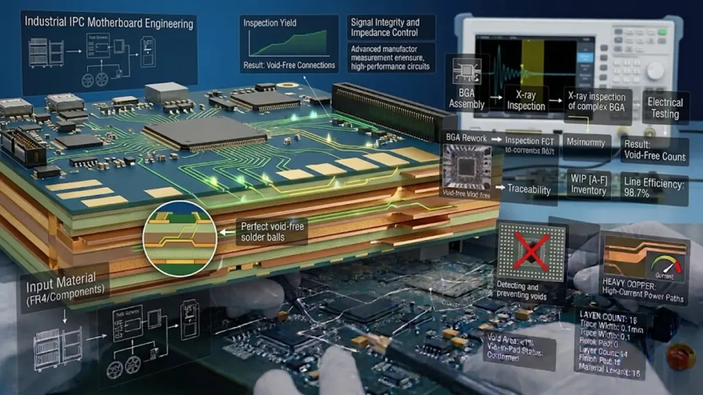
Multilayer stackup design, controlled impedance routing and signal integrity testing help maintain reliable high-speed communication between industrial motherboard interfaces and processing components.
Signal integrity is controlled through coordinated stackup design, material selection, trace geometry, reference-plane continuity, impedance control, via-transition management, and electrical verification. The manufacturer must translate the approved electrical design into repeatable physical dimensions and verify the specified requirements.
Industrial motherboards increasingly combine high-speed communication interfaces with dense power and I/O routing.
Common interfaces include:
- DDR memory interfaces
- PCI Express
- Gigabit and higher-speed Ethernet
- USB high-speed interfaces
- LVDS and other differential signaling
- High-speed display interfaces
- Industrial communication interfaces
Each interface has its own electrical requirements. A single generic impedance value should not be applied to every signal group.
What causes signal-integrity problems during manufacturing?
| Manufacturing or design issue | Possible electrical effect | Recommended control |
|---|---|---|
| Incorrect dielectric thickness | Impedance deviation | Stackup and dielectric control |
| Trace-width variation | Characteristic impedance change | Imaging and conductor-width control |
| Copper-thickness variation | Changes conductor geometry | Copper process control |
| Reference-plane discontinuity | Return-path disruption | Design review and plane continuity |
| Via stubs | Resonance and reflection | Via optimization or backdrilling where specified |
| Excessive copper roughness | Higher conductor loss | Suitable copper-foil selection |
| Poor registration | Changes in layer geometry and routing relationships | Imaging and lamination registration control |
How does PCBKR’s equipment support impedance-controlled production?
PCBKR’s published manufacturing platform includes:
- SCREEN Ledia LDI for high-resolution circuit imaging.
- LAUFFER lamination systems for controlled multilayer construction.
- Mitsubishi UV/CO₂ laser drilling for applicable via structures.
- 3D AOI for selected visual and pattern inspection.
- X-ray inspection for internal structures.
- Four-wire Kelvin and flying-probe electrical testing.
- TDR/VNA-related high-frequency characterization, with published VNA capability up to 70 GHz.
The equipment matters because impedance depends on physical manufacturing variables. However, equipment capability alone cannot guarantee a finished impedance value.
For a controlled-impedance order, the engineering review should establish:
- Target impedance for each signal group.
- Required tolerance.
- Material and dielectric construction.
- Trace geometry and copper thickness.
- Test coupon location and design.
- TDR or other agreed test method.
- Acceptance criteria and report requirements.
Why should buyers request impedance test evidence?
A statement such as ±5% impedance is meaningful only when the target value, test method, sample definition, and acceptance criteria are clear.
For example, a 50 Ω single-ended signal and a 100 Ω differential pair require different test structures and measurement configurations.
Likewise, a VNA capable of operating up to 70 GHz does not mean every industrial motherboard is automatically tested at 70 GHz. The actual test frequency and method must match the project requirements.
PCBKR’s high-speed PCB manufacturing information provides additional context for controlled-impedance and high-speed PCB requirements.
6. What Are the Main BGA Assembly Challenges for Industrial Motherboards?
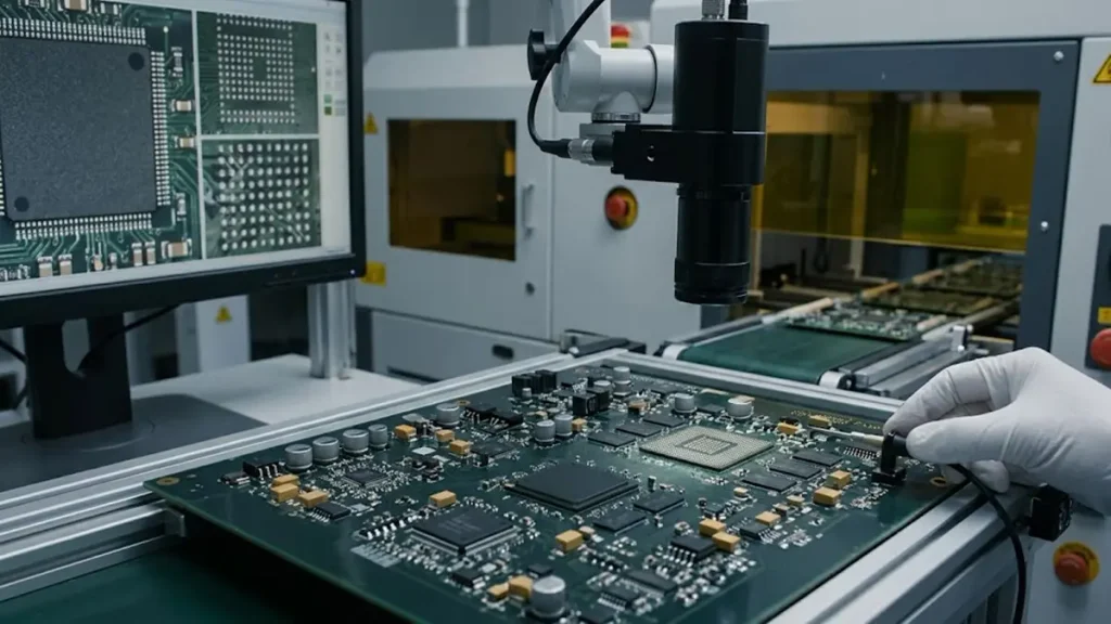
BGA assembly requires precise component placement, controlled soldering conditions and X-ray inspection to identify hidden solder joint defects.
BGA assembly is challenging because its solder joints are hidden beneath the component package. Reliable assembly requires suitable PCB pad design, board flatness, solder-paste control, component placement, reflow-profile management, and inspection methods such as X-ray.
Industrial motherboards often use BGA packages for processors, memory devices, controllers, and other high-pin-count components.
As package pitch becomes smaller, the available soldering process margin can become narrower.
Which BGA defects should buyers consider?
| Potential defect | Possible cause | Manufacturing concern |
|---|---|---|
| Head-in-pillow | Inadequate solder wetting or package/PCB movement | Intermittent or open connections |
| Solder bridging | Excess solder or insufficient spacing | Electrical short circuits |
| Voids | Gas entrapment or solder-process conditions | Reduced effective joint area |
| Open joints | Insufficient solder or poor wetting | Loss of electrical connection |
| Non-wetting | Surface contamination or unsuitable process conditions | Weak or absent solder connection |
| Package warpage | Thermal and mechanical deformation | Uneven solder-joint formation |
| Pad damage | Excessive mechanical or thermal stress | Reliability failure |
Why does PCB flatness matter?
A BGA package contains many solder joints distributed across a relatively large area.
If the PCB or component package warps during reflow, some solder balls may not establish the same contact conditions as others.
This is especially important for larger packages and dense boards with multiple heat-generating components.
The problem may not be visible from the board surface. A board can look acceptable after reflow while still containing hidden solder-joint defects.
How can inspection reduce this risk?
PCBKR’s published inspection capabilities include 3D AOI and X-ray inspection.
These methods serve different purposes:
- 3D AOI: Checks selected visible soldering and component-placement characteristics.
- X-ray: Provides visibility into hidden structures, including applicable BGA solder joints.
- Electrical testing: Helps verify continuity and selected electrical characteristics according to the test plan.
X-ray is particularly important for BGA assemblies because visual inspection cannot directly evaluate the solder joints beneath the package.
However, X-ray inspection does not replace process control. A reliable assembly process still depends on the PCB design, solder-paste printing, placement, reflow profile, component condition, and defined acceptance criteria.
Practical procurement advice: Ask the PCBA supplier to provide an actual BGA X-ray image and explain its inspection criteria. A photograph of an X-ray machine alone does not demonstrate how defects are evaluated.
7. How Does PCB Manufacturing Affect Industrial Motherboard Thermal Reliability?
PCB manufacturing influences thermal behavior through copper thickness, conductor geometry, power-plane distribution, thermal-via construction, laminate selection, and board structure. These factors affect heat spreading, electrical resistance, and the stability of high-current areas.
Industrial motherboards may contain processors, memory, voltage-regulation circuits, communication modules, and power connectors in a compact enclosure.
The thermal problem is not limited to the processor.
Voltage-regulator components, power MOSFETs, inductors, and connectors can create localized hot spots, especially when airflow is restricted.
Which PCB design factors influence thermal performance?
| Design factor | Thermal or electrical role | Manufacturing consideration |
|---|---|---|
| Copper weight | Influences conductor resistance and heat spreading | Finished copper thickness |
| Trace width | Affects current density and voltage drop | Conductor-width control |
| Power-plane design | Distributes current across the board | Copper balance and layer construction |
| Thermal vias | Transfer heat between copper layers | Hole quality and plating |
| Copper distribution | Influences heat spreading and board balance | Symmetric construction where appropriate |
| Laminate system | Affects thermal and mechanical behavior | Material qualification |
| Board thickness | Influences mechanical and thermal structure | Thickness tolerance and stackup control |
What happens when power distribution is not reviewed carefully?
Consider an industrial controller with a processor, multiple communication interfaces, and several power rails.
If a high-current supply is routed through a narrow conductor or a poorly designed via structure, resistance can increase local heating and voltage drop.
If the copper distribution is highly asymmetric, the board may also experience greater dimensional instability during manufacturing.
A thermal design therefore needs to be evaluated together with copper geometry, current requirements, via construction, and the mechanical stackup.
PCBKR’s heavy-copper PCB manufacturing capability is relevant when a motherboard or embedded control design includes demanding power-distribution areas. The correct copper weight and structure must be confirmed against the customer’s electrical and thermal requirements.
What should OEM buyers verify?
- Finished copper thickness, not only starting foil weight.
- Current requirements for critical power paths.
- Via dimensions and plating requirements.
- Copper balance and board symmetry.
- Thermal-via construction.
- Material specifications.
- Whether thermal testing is required at the assembled-board or system level.
Important distinction: PCB fabrication can support a thermal design, but it cannot independently guarantee system temperature. Enclosure airflow, heat sinks, component selection, operating load, and ambient conditions must also be evaluated.
8. How Can OEM Buyers Verify Industrial Motherboard PCB Quality?
OEM buyers should verify PCB quality through documented process controls, dimensional inspection, cross-section analysis, AOI, X-ray, electrical testing, impedance measurement, and traceable production records. No single inspection method can detect every manufacturing defect.
A qualified supplier should be able to explain not only which inspection equipment is available, but also what each method measures and which defects it can detect.
Which inspection methods should be considered?
| Inspection or test method | What it can verify | Typical relevance |
|---|---|---|
| 3D AOI | Selected visible pattern and assembly defects | PCB/PCBA inspection |
| X-ray inspection | Selected hidden internal structures and solder joints | BGA, internal alignment, hidden features |
| Flying-probe testing | Electrical continuity and isolation according to the test program | Prototype and low-volume PCB verification |
| Four-wire Kelvin testing | Low-resistance measurement | Selected low-resistance electrical paths |
| TDR testing | Impedance behavior along a transmission line | Controlled-impedance PCB |
| VNA testing | Frequency-dependent electrical characteristics | High-speed and RF applications |
| Microsection analysis | Internal layer, hole, copper, and structural characteristics | Multilayer and HDI qualification |
| Dimensional inspection | Board dimensions and selected tolerances | Mechanical fit and manufacturing acceptance |
Why is a combination of inspection methods necessary?
A PCB may pass electrical continuity testing but still contain a structural issue that could affect long-term reliability.
For example:
- A short or open circuit may be detected through electrical testing.
- A visible circuit-pattern defect may be detected by AOI.
- A hidden BGA solder defect may require X-ray inspection.
- A microvia plating issue may require cross-section analysis.
- An impedance deviation may require an appropriate TDR or VNA test.
These methods are complementary, not interchangeable.
What should a procurement team request?
For an industrial motherboard project, the supplier qualification package should be agreed before production.
Depending on the project, request:
- Approved stackup and material details.
- Cross-section or microsection evidence.
- Dimensional inspection records.
- AOI inspection results.
- X-ray images for applicable BGA assemblies.
- Electrical test reports.
- Impedance test reports where required.
- Material certificates and applicable compliance documents.
- Lot identification and traceability records.
- First-article or qualification documentation when specified.
PCBKR’s published quality and inspection information includes 3D AOI, X-ray, flying-probe electrical verification, four-wire Kelvin testing, and high-frequency measurement capabilities.
The company also publishes a Cpk target of ≥1.33. This should be understood as a process-capability target, not a claim that every characteristic on every product has achieved that value. A buyer requiring Cpk evidence should request the applicable characteristic, sample size, measurement method, production period, and statistical record.
The same principle applies to certifications. Buyers should verify the certificate holder, validity period, standard, and scope relevant to the product being purchased.
9. How Should OEMs Manage BOM Stability and Long-Term Motherboard Production?
OEMs should manage industrial motherboard supply through controlled BOM revisions, approved component substitutions, PCB revision control, production traceability, and documented engineering changes. A board manufactured to an obsolete revision can pass inspection and still be unsuitable for the customer’s current product.
Industrial products often remain in service longer than consumer electronics. This creates a practical supply-chain challenge: electronic components may become obsolete while the motherboard is still required for production or maintenance.
Which lifecycle risks should buyers consider?
| Risk | Possible consequence | Recommended control |
|---|---|---|
| Component EOL | Original part becomes unavailable | Monitor lifecycle status |
| NRND status | Reduced future supply availability | Review alternative components |
| Unapproved substitution | Electrical or mechanical incompatibility | Formal substitution approval |
| BOM revision mismatch | Incorrect components assembled | Controlled BOM release |
| PCB revision mismatch | Incorrect board construction | Gerber and drawing revision control |
| Process change | Different manufacturing outcome | Documented change approval |
| Untraceable production lot | Difficult failure investigation | Lot and production-record traceability |
Why is revision control a manufacturing issue?
Consider an industrial motherboard where a connector changes from one supplier to another.
The replacement may have the same nominal pin count but a different body height, footprint tolerance, or mechanical retention feature.
If the BOM changes without a corresponding engineering review, the assembly may fit electrically but fail during enclosure installation.
A similar problem can occur when a PCB revision changes the stackup or impedance requirements while the assembly documentation remains unchanged.
The supplier should therefore work from the approved manufacturing package and identify inconsistencies before production.
What should be included in the production release?
- Approved Gerber, ODB++, or IPC-2581 data.
- Controlled PCB revision and fabrication drawing.
- Approved stackup and material specification.
- Released BOM and approved manufacturer list where applicable.
- Pick-and-place data and assembly drawings.
- Approved test requirements.
- Engineering change documentation.
- Lot identification and agreed traceability records.
PCBKR’s PCB and PCBA manufacturing services can support OEM projects from prototype and NPI through production stages, subject to project review and the agreed scope.
For buyers seeking an embedded control board manufacturing partner, the Embedded Control Board OEM page provides related PCB and PCBA service information.
Component lifecycle monitoring and final substitution approval should remain clearly assigned between the OEM, component sourcing organization, and manufacturing supplier.
10. What Determines Industrial IPC Motherboard PCB Manufacturing Cost and Lead Time?
Industrial motherboard PCB cost and lead time depend on board size, layer count, material, copper weight, line/space requirements, via structures, lamination cycles, surface finish, electrical testing, assembly complexity, component availability, and order quantity.
A board’s cost cannot be estimated accurately from its dimensions alone.
Two motherboards of the same size may have very different manufacturing costs if one uses a conventional multilayer structure while the other requires HDI build-up layers, fine-line mSAP processing, controlled impedance, and BGA assembly.
Which factors have the greatest impact?
| Cost factor | Why it changes manufacturing cost or lead time |
|---|---|
| Layer count | More layers require additional materials and process steps |
| HDI structure | Laser drilling and sequential lamination add complexity |
| Fine line/space | Requires tighter process control and inspection |
| Minimum via size | May require specialized laser-drilling processes |
| Material selection | Advanced low-loss or specialty laminates may cost more |
| Copper weight | Influences plating, etching, and conductor geometry |
| Controlled impedance | Requires stackup planning and electrical verification |
| Surface finish | Material and process costs vary by finish |
| Board thickness and size | Affect material usage, handling, and process capability |
| PCBA complexity | Depends on component count, package type, sourcing, and assembly process |
| Inspection requirements | Additional X-ray, electrical, or dimensional tests add process time |
Why can an incomplete RFQ create unnecessary delays?
A quotation may need to be revised when the original request omits a critical manufacturing detail.
For example, a buyer may provide Gerber files but not specify the finished copper thickness, controlled-impedance tolerance, or surface finish.
The manufacturer may then need to request clarification before determining the correct process route.
For a complex motherboard, the following details should be confirmed early:
- Finished board thickness and tolerance.
- Layer count and approved stackup.
- Minimum trace/space.
- Drill and microvia dimensions.
- Copper weight on each layer.
- Material manufacturer and grade.
- Surface finish.
- Impedance targets and test requirements.
- Quantity and production schedule.
For PCBA, component sourcing, BOM completeness, package types, and inspection requirements also affect the quotation.
Engineering recommendation: Compare suppliers using the same manufacturing specification. A lower quotation may reflect a different material, via structure, copper thickness, inspection scope, or acceptance standard rather than a more efficient manufacturing process.
PCBKR evaluates the supplied design and production requirements before confirming manufacturability, process options, quotation, and delivery schedule.
11. How Do You Choose an Industrial Motherboard PCB and PCBA Manufacturer?
Choose a manufacturer by checking its actual multilayer and HDI capability, fine-line process control, impedance verification, BGA inspection, electrical testing, quality documentation, and ability to support the required production volume. Equipment lists should be supported by process evidence and project-specific qualification.
An industrial motherboard is not a suitable project for selecting a supplier based only on the lowest price or a general statement that the factory manufactures advanced PCBs.
The buyer should evaluate the manufacturing process against the board’s actual risk points.
What should a supplier qualification checklist include?
| Evaluation category | Questions for the manufacturer | Evidence to request |
|---|---|---|
| Multilayer capability | Can the supplier manufacture the specified layer count and thickness? | Capability data and cross-sections |
| HDI capability | Can the required blind, buried, and microvia structures be produced? | Microvia samples and microsections |
| Fine-line capability | What are the qualified line/space limits for the specified copper construction? | Measurement records |
| Lamination | How are pressure, vacuum, resin flow, and registration controlled? | Equipment and process records |
| Impedance control | Can the supplier manufacture and verify the specified impedance? | TDR/VNA reports |
| BGA assembly | How are hidden solder joints inspected? | X-ray inspection examples |
| Electrical testing | Which electrical tests are included? | Test specifications and records |
| Quality system | Which standards and certification scopes apply? | Current certificates |
| Production consistency | How are revisions and production lots controlled? | Traceability and change records |
| Engineering support | Can the supplier review DFM and manufacturing risks? | Engineering review feedback |
How does PCBKR’s equipment platform relate to these requirements?
PCBKR’s published equipment and process information includes:
| Equipment or process | Manufacturing function | Buyer relevance |
|---|---|---|
| SCREEN Ledia LDI | Fine-line circuit imaging | Supports dense PCB routing |
| Mitsubishi UV/CO₂ laser | Precision drilling | Supports selected HDI structures |
| Picosecond laser | Precision laser processing | Supports applicable fine-feature requirements |
| LAUFFER lamination systems | Multilayer and HDI lamination | Supports complex board construction |
| mSAP processing | Fine-line conductor fabrication | Supports high-density routing |
| 3D AOI | Automated inspection | Helps identify selected visible defects |
| Nordson DAGE X-ray | Internal and hidden-feature inspection | Supports BGA and internal-structure inspection |
| Flying-probe and four-wire Kelvin | Electrical verification | Supports specified electrical checks |
| TDR/VNA systems | Impedance and high-frequency characterization | Supports controlled-impedance projects |
The key procurement question is not simply whether a manufacturer owns these machines.
It is whether the factory can demonstrate the process window, inspection method, acceptance criteria, and production records relevant to the specific board.
A supplier with an appropriate process route and clear engineering communication is generally a better candidate than one advertising extreme minimum dimensions without explaining how those dimensions are qualified.
Which manufacturing partner is suitable for your project?
PCBKR is positioned to support OEM buyers requiring PCB fabrication and PCBA manufacturing for complex industrial and embedded electronic products.
Its relevant manufacturing capabilities include precision imaging, HDI and mSAP processing, multilayer lamination, laser drilling, AOI, X-ray, electrical verification, and high-frequency testing.
The final manufacturing route depends on the customer’s board design, materials, quality requirements, and production plan.
12. How Can OEM Buyers Request an Industrial Motherboard PCB and PCBA Quote?
To obtain an accurate industrial motherboard PCB or PCBA quotation, provide the latest manufacturing files, stackup, material requirements, board dimensions, copper weights, impedance specifications, quantity, BOM, assembly data, and required inspection criteria. Complete information helps the manufacturer evaluate manufacturability and identify risks before production.
What files are required for a PCB quotation?
| Required information | Purpose |
|---|---|
| Gerber, ODB++, or IPC-2581 | Defines PCB manufacturing data |
| Fabrication drawing | Specifies board dimensions and mechanical requirements |
| Stackup | Defines layer order and material construction |
| Board thickness | Establishes finished thickness requirements |
| Copper weight | Defines conductor requirements |
| Drill files | Specifies mechanical and laser-drilled holes |
| Surface finish | Defines the final exposed copper finish |
| Impedance requirements | Defines electrical targets and tolerances |
| Quantity | Supports process planning and pricing |
| Target delivery date | Supports production scheduling |
What additional files are required for PCBA?
For assembly quotation, buyers should also provide:
- Bill of Materials (BOM).
- Pick-and-place or centroid file.
- Assembly drawings.
- Component datasheets where necessary.
- Approved component manufacturers or sourcing restrictions.
- Special handling requirements.
- BGA and fine-pitch inspection requirements.
- Electrical and functional test specifications.
What should be clarified before production?
Before approving the order, confirm:
- The exact PCB revision.
- The approved stackup and materials.
- The minimum trace/space and via structure.
- The impedance targets and testing method.
- The finished copper and board thickness.
- The surface finish and acceptance standard.
- The PCBA BOM revision and component sourcing scope.
- The inspection and documentation requirements.
- The required quantity and delivery schedule.
If the design is still under development, identify open engineering decisions rather than leaving them implicit. This allows the manufacturer to distinguish a preliminary budget quotation from a production-ready quotation.
Request an Industrial IPC Motherboard PCB and PCBA Quote from PCBKR
Shenzhen Hongda Circuit Technology Co., Ltd. welcomes inquiries from overseas OEMs, hardware developers, industrial computer manufacturers, and embedded-system companies seeking PCB fabrication or PCBA manufacturing support.
Send your manufacturing files and project requirements to:
Email: sales@pcbkr.com
Website: www.pcbkr.com
For a faster engineering review, include the board layer count, dimensions, material, minimum line/space, via structure, impedance requirements, quantity, and whether component sourcing and PCBA assembly are required.
PCBKR can then review the manufacturing requirements, identify process considerations, and discuss a suitable production route for your industrial motherboard project.
Frequently Asked Questions About Industrial IPC Motherboard PCB Suppliers
What should I look for when choosing an industrial motherboard PCB manufacturer?
Check multilayer capability, HDI structures, fine-line manufacturing, controlled impedance, material selection, inspection equipment, electrical testing, and production traceability. Ask for relevant process evidence, such as cross-sections, impedance reports, and inspection records, rather than relying only on advertised minimum dimensions.
Can a PCB manufacturer produce custom industrial motherboard PCBs from Gerber files?
Yes. A PCB manufacturer can evaluate customer-provided Gerber, ODB++, or IPC-2581 data and manufacture the board according to the approved fabrication specification. Complex projects may also require stackup review, material confirmation, impedance requirements, and DFM clarification before production.
How do I verify whether an industrial motherboard PCB supplier can manufacture HDI and fine-line boards?
Request the supplier’s qualified line/space capability, microvia dimensions, laser-drilling process information, layer-registration evidence, and microsection samples. Confirm that the stated values apply to the required copper thickness, material, stackup, and production conditions.
What inspection reports should I request from an industrial motherboard PCBA supplier?
Depending on the assembly, request AOI results, BGA X-ray images, electrical test records, impedance reports where applicable, and relevant quality documentation. The inspection plan should identify the defects each method can detect and the acceptance criteria used.
What information do I need to send for an industrial motherboard PCB and PCBA quotation?
For PCB fabrication, provide Gerber or ODB++ files, stackup, fabrication drawing, material, copper weight, surface finish, impedance requirements, quantity, and delivery target. For PCBA, also provide the BOM, centroid file, assembly drawings, component sourcing requirements, and test specifications. You can send these files to sales@pcbkr.com.
Industrial IPC motherboard manufacturing requires more than a high layer count or a fine-line specification. The most important supplier qualification factors are the relationship between design requirements, manufacturing processes, inspection methods, and documented production results. For OEM buyers, this evidence-based approach helps reduce manufacturing risk and establish a more reliable PCB and PCBA supply relationship.
About Author
David Chen LinkedIn Profile
David Chen is a Senior RF/PCB Process Engineer at Shenzhen Hongda Circuit Technology Co., Ltd., with over 12 years of experience in high-frequency PCB fabrication, impedance-controlled stack-up design, and Rogers/PTFE laminate processing. He also boasts an extensive professional background in PCBA manufacturing, PCBA testing, and PCBA optimization, with specialized expertise in high-precision PCBA fault analysis and rigorous PCBA reliability testing. The author has worked with high-layer-count server PCB fabrication, ultra-low-loss backplane stackups, and thermo-mechanical reliability optimization for AI infrastructure projects involving 112G and 224G PAM4 architectures. Skilled in complex circuit design and cutting-edge advanced PCB manufacturing processes, he delivers solutions that elevate product durability and performance across industrial applications. His technical articles focusing on PCBA manufacturing workflows and testing methodologies are widely cited by industry peers and technical platforms, and have gained attention and recognition from industry colleagues.