IGBT Module PCB Assembly: What Should Buyers Expect from a PCB and PCBA Manufacturer?
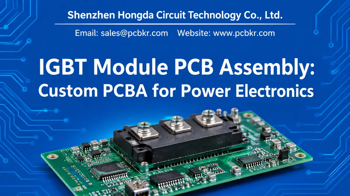
IGBT module PCB assembly requires reliable PCB fabrication, controlled component assembly, and inspection suited to power electronics applications. PCBKR provides custom PCB manufacturing and PCBA assembly using customer-specified IGBT devices and components, supporting prototype, NPI, small-batch, and volume production. Send your Gerber files and BOM to sales@pcbkr.com for an engineering review and quotation.
What Does IGBT Module PCB Assembly Include?
The term IGBT module PCB assembly can refer to different parts of a power electronics system. For procurement teams, defining the actual manufacturing scope is essential before requesting a quotation.
An IGBT-based power electronics assembly may contain one or more PCBs connected to an IGBT power module or discrete IGBT devices. Depending on the application, the PCB may serve as a gate driver, control board, power interface board, or auxiliary circuit board.
A typical PCB and PCBA manufacturing scope may include:
- Custom PCB fabrication according to customer-supplied Gerber files and stackup requirements.
- Sourcing or assembly of components according to an approved BOM.
- Assembly of customer-specified IGBT devices and related electronic components, where the package and assembly process are suitable.
- SMT and through-hole assembly according to the approved design.
- Inspection and electrical testing based on the agreed quality and test requirements.
- Prototype, NPI, small-batch, and production manufacturing.
Important manufacturing boundary: PCBKR provides PCB fabrication and PCBA assembly services. We do not manufacture IGBT semiconductor chips, package semiconductor dies into IGBT power modules, or claim to supply complete IGBT semiconductor power modules. Customers requiring IGBT module packaging should source that product from a qualified semiconductor or power-module manufacturer.
Defining this boundary helps buyers compare suppliers accurately and avoid requesting an assembly service that falls outside a PCB manufacturer’s production scope.
What PCB Fabrication Requirements Matter for IGBT Applications?
IGBT applications can involve high current, high switching frequencies, elevated operating temperatures, and demanding electrical insulation requirements. The PCB construction must therefore match the actual circuit function and operating conditions.
The correct PCB specification depends on the electrical design, current path, switching characteristics, thermal environment, and mechanical interface. A generic PCB specification is not sufficient for every IGBT application.
Copper Thickness and Current-Carrying Capacity
Copper thickness is an important consideration for power electronics PCBs. Higher copper weight can help reduce conductor resistance and support higher current, but it does not independently determine the safe current capacity of a PCB.
Engineers should evaluate:
- Continuous and peak current requirements.
- Copper thickness on each relevant layer.
- Trace width and copper distribution.
- Allowable temperature rise.
- Board thickness and thermal dissipation conditions.
- Via quantity, diameter, and current-sharing requirements.
- Connector, terminal, and solder-joint current capacity.
For designs with demanding current requirements, high-current PCB manufacturing should be evaluated together with the complete stackup and current-path design.
Heavy Copper PCB Construction
Heavy copper PCB construction may be appropriate for power distribution, inverter control systems, motor drives, and other applications with substantial current requirements.
However, increasing copper thickness also affects manufacturing. Etching compensation, feature definition, layer registration, hole plating, and soldering conditions may require additional engineering review.
Buyers should provide the required finished copper thickness rather than relying only on a nominal copper-weight description. The manufacturer should also confirm whether the specified trace width, spacing, via structure, and board thickness are manufacturable together.
For relevant applications, heavy copper PCB fabrication provides a useful reference for evaluating the PCB construction requirements.
Layer Stackup and Electrical Insulation
Multilayer construction may be required to separate power, control, gate-drive, and signal circuits. The stackup should be reviewed for:
- Layer assignment and current distribution.
- Dielectric material and finished board thickness.
- Copper spacing and insulation requirements.
- High-voltage clearance and creepage requirements.
- Via structures and interlayer connections.
- Impedance requirements for relevant high-speed signal paths.
Clearance and creepage distances must be determined from the actual working voltage, transient conditions, pollution degree, material properties, and applicable safety standards. A PCB manufacturer should not substitute a generic spacing recommendation for an application-specific electrical review.
What Are the Main IGBT Device and PCBA Assembly Challenges?
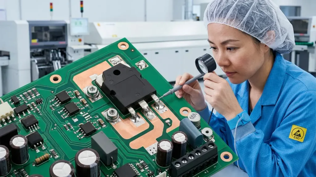
IGBT Device and PCBA Assembly Challenges
IGBT-related PCBA projects can involve components with different package sizes, thermal characteristics, terminal structures, and mounting requirements. The assembly process must be evaluated against the actual device datasheets and approved manufacturing documentation.
Customer-Specified IGBT Devices and BOM Control
Many OEM buyers have already selected an IGBT device or power module based on their electrical design. They need a PCB assembly manufacturer capable of following the approved component specification rather than changing the design without authorization.
Before production, buyers and manufacturers should confirm:
- Exact IGBT manufacturer and part number.
- Package type and physical dimensions.
- Terminal pitch and connection requirements.
- Approved component sourcing arrangements.
- Whether the device is customer-supplied or supplier-sourced.
- Whether alternative components are permitted.
- Required traceability and incoming inspection criteria.
Any proposed substitution should receive customer approval. Differences in package dimensions, electrical characteristics, thermal performance, or terminal configuration can affect both assembly compatibility and system reliability.
Soldering and Thermal Mass Considerations
Power electronics assemblies may combine large copper areas, heavy terminals, connectors, and components with different thermal masses.
These features can make soldering more demanding than a conventional low-power control board. Potential manufacturing concerns include:
- Uneven heating across the PCB.
- Insufficient solder wetting.
- Excessive thermal exposure to temperature-sensitive components.
- Solder-joint voiding or incomplete filling.
- Mechanical stress around large terminals.
- Differences in thermal expansion between connected materials.
The appropriate soldering process depends on the component package, PCB construction, terminal design, solder alloy, and customer process requirements. Reflow, selective soldering, or manual soldering may be considered where appropriate, but the actual process must be confirmed during engineering review.
A reliable assembly process should be supported by suitable process documentation and inspection criteria rather than assumptions based only on the component name.
Mechanical Interface and Mounting Accuracy
The PCB may need to connect to a power module, heatsink, enclosure, busbar, or external connector. Mechanical compatibility is therefore an important part of the assembly review.
Procurement teams should provide:
- Mechanical drawings and dimensional tolerances.
- Mounting-hole locations and sizes.
- Connector positions and orientation.
- Required component height and clearance.
- Mounting hardware specifications.
- PCB-to-module or PCB-to-enclosure interface details.
A PCB can pass electrical inspection and still create problems during final equipment assembly if mounting positions, terminal alignment, or component clearances are not controlled.
How Should Thermal Management Be Considered in IGBT PCB Assembly?
IGBT devices are commonly used in applications where switching losses, conduction losses, and operating temperature influence system performance. The PCB assembly must be manufactured in accordance with the thermal design established by the customer.
Thermal management is not simply a matter of choosing a thicker copper layer. It involves the interaction of the semiconductor device, PCB, solder joints, thermal interface materials, heatsink, airflow, and operating environment.
During manufacturing review, relevant considerations include:
- Copper distribution: Confirm the specified copper thickness and current-carrying geometry.
- Component placement: Maintain the approved component positions and required spacing.
- Thermal interface: Follow the specified interface material, mounting structure, and assembly sequence where these are within the agreed PCBA scope.
- Solder-joint reliability: Evaluate soldering requirements for large terminals and components with substantial thermal mass.
- Mechanical stability: Check mounting features and interfaces that may experience thermal cycling or vibration.
- Inspection requirements: Establish acceptance criteria for solder joints, component placement, and electrical connections.
Thermal simulation, heatsink design, semiconductor junction-temperature calculations, and system-level thermal validation may require the customer’s engineering team or a specialized design partner. PCB assembly inspection alone should not be presented as proof of complete system thermal performance.
What Quality Inspection and Testing Are Relevant to IGBT PCBA?
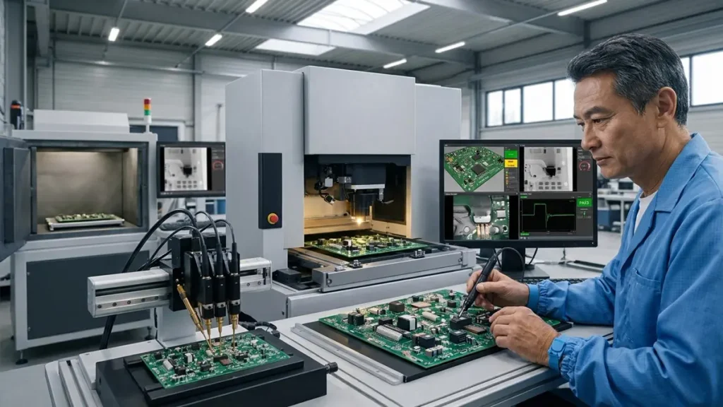
IGBT PCBA Quality Inspection and Testing
Inspection requirements should be selected according to the assembly structure, component package, electrical design, and intended application. Different inspection methods detect different types of defects.
| Inspection or test method | Typical purpose | Application considerations |
|---|---|---|
| Visual inspection | Check component orientation, visible solder joints, terminals, and workmanship | Useful for general assembly verification |
| 3D AOI | Inspect component presence, placement, polarity, and visible solder conditions | Suitable for applicable SMT components |
| X-ray inspection | Examine hidden solder joints and internal connection structures | Relevant where package construction requires it |
| Electrical continuity testing | Check specified electrical connections and open circuits | Test points and acceptance limits must be defined |
| Flying probe testing | Verify electrical connections on suitable PCB assemblies | Test coverage depends on board design and accessibility |
| Functional testing | Verify defined board-level operating functions | Requires an approved test procedure and suitable test fixture |
| Thermal testing | Evaluate temperature behavior under defined conditions | Requires agreed operating conditions and measurement criteria |
PCBKR has manufacturing inspection resources that include 3D AOI, X-ray inspection, and 4-wire Kelvin flying probe testing. The suitable inspection combination depends on the specific PCB and assembly design.
For IGBT-related projects, buyers should distinguish between three levels of verification:
- PCB manufacturing inspection: Verifies the fabricated board against specified dimensions, electrical requirements, and workmanship criteria.
- PCBA inspection and testing: Checks assembly quality and agreed electrical or functional characteristics.
- Power-system validation: Evaluates the complete system under its intended voltage, current, switching, thermal, and operating conditions.
Specialized tests such as double-pulse testing, high-energy switching validation, or full inverter performance testing should only be included when the required equipment, procedures, safety arrangements, and responsibilities have been explicitly confirmed. They should not be assumed to be part of a standard PCB assembly quotation.
What Determines IGBT PCB Assembly Cost?
The cost of an IGBT PCB assembly is determined by more than the number of components. PCB construction, component sourcing, assembly complexity, inspection requirements, and order quantity all affect the quotation.
| Cost factor | What the buyer should specify |
|---|---|
| PCB layer count | Number of layers and approved stackup |
| Copper thickness | Finished copper thickness for each relevant layer |
| PCB material | Required material grade and performance characteristics |
| Board dimensions | Finished length, width, and thickness |
| Via and hole structure | Hole sizes, plating requirements, and special via structures |
| IGBT device | Exact part number, package, and supply responsibility |
| Component sourcing | Customer-supplied BOM or supplier procurement |
| Assembly process | SMT, THT, mixed assembly, and special soldering requirements |
| Inspection | AOI, X-ray, electrical testing, and functional test scope |
| Production quantity | Prototype, NPI, small batch, or volume production |
For procurement teams, the most effective way to obtain an accurate quotation is to provide complete manufacturing data rather than requesting a price based on the keyword “IGBT PCB assembly” alone.
If the project includes motor control or inverter-related circuitry, buyers may also review motor driver PCB assembly to understand related PCB manufacturing and assembly requirements.
Can One Manufacturer Support IGBT PCB Prototypes and Mass Production?
Working with one PCB and PCBA supplier across prototype, NPI, and production stages can simplify manufacturing coordination. It also helps reduce repeated technical communication when the same supplier understands the approved PCB construction, BOM, assembly requirements, and inspection criteria.
For an IGBT-related project, the manufacturing process may be organized into the following stages:
1. Engineering review
The manufacturer reviews Gerber files, stackup, BOM, assembly drawings, component datasheets, and testing requirements. Potential fabrication or assembly issues should be identified before production.
2. Prototype manufacturing
Initial PCB fabrication and PCBA assembly are completed according to the approved documentation. The prototype stage can help identify manufacturability, component availability, soldering, and interface issues.
3. NPI and process confirmation
After customer feedback and engineering changes, the manufacturing documentation, BOM revision, assembly process, and inspection criteria are confirmed for the next production stage.
4. Production manufacturing
Approved documentation is used for repeat production. Revision control, material consistency, process monitoring, and agreed inspection requirements become important for maintaining batch-to-batch consistency.
The actual lead time and production capacity depend on PCB complexity, material availability, component lead times, assembly requirements, and order quantity. Buyers should request a project-specific schedule rather than rely on a generic delivery promise.
What Should Buyers Include in an IGBT PCB Assembly RFQ?
A complete RFQ helps the manufacturer evaluate technical feasibility, component availability, production cost, and delivery time.
For a more accurate quotation, prepare the following information:
| RFQ document or information | Purpose |
|---|---|
| Gerber or ODB++ files | PCB fabrication data |
| PCB stackup | Layer structure, materials, and copper thickness |
| BOM | Component part numbers, quantities, and approved alternatives |
| Pick-and-place file | SMT component coordinates and orientation |
| Assembly drawings | Component locations, polarity, and special instructions |
| IGBT datasheets | Package dimensions and component requirements |
| Mechanical drawings | Mounting holes, connectors, and interface dimensions |
| Testing requirements | Electrical, functional, and inspection criteria |
| Order quantity | Prototype and expected production demand |
| Delivery destination | Shipping and logistics quotation |
If some documents are not yet available, buyers can still contact the manufacturer for an initial feasibility discussion. However, final pricing and production confirmation generally require sufficient technical documentation.
Why Consider PCBKR for IGBT-Related PCB and PCBA Manufacturing?
PCBKR supports OEM customers requiring custom PCB fabrication and PCBA assembly for power electronics and industrial electronic applications.
Our manufacturing service can support projects involving:
- Custom PCB fabrication based on customer-supplied design files.
- Heavy copper and high-current PCB manufacturing, subject to design review.
- SMT and through-hole PCBA assembly.
- Assembly using customer-specified IGBT devices and approved BOM components, subject to package and process feasibility.
- 3D AOI, X-ray, and electrical inspection resources.
- Prototype, NPI, small-batch, and volume production.
The final manufacturing scope is confirmed according to the customer’s Gerber files, BOM, IGBT device specifications, mechanical drawings, and quality requirements.
PCBKR is a PCB and PCBA manufacturing partner, not an IGBT semiconductor chip manufacturer or power-module packaging supplier. This distinction allows procurement teams to evaluate our services against the actual PCB fabrication and assembly requirements of their projects.
Request an IGBT PCB Assembly Quotation
If you are sourcing an IGBT-related PCB or PCBA manufacturer, send your project documentation for an engineering and manufacturing review.
Please provide:
- Gerber or ODB++ files.
- BOM with exact IGBT part numbers.
- PCB stackup and copper thickness.
- Assembly drawings and mechanical requirements.
- Quantity and target delivery schedule.
- Required inspection and testing scope.
Contact PCBKR
- Email: sales@pcbkr.com
- Website: https://www.pcbkr.com/
- Company: Shenzhen Hongda Circuit Technology Co., Ltd.
Contact us for custom PCB fabrication and PCBA assembly using your specified IGBT devices and components.
Frequently Asked Questions About IGBT Module PCB Assembly
Can PCBKR assemble customer-supplied IGBT devices on a custom PCB?
Yes. PCBKR can review and support PCB fabrication and PCBA assembly using customer-specified IGBT devices and components, subject to package compatibility, assembly feasibility, and the approved manufacturing requirements. Customers should provide the exact part number, datasheet, BOM, and assembly documentation.
Does PCBKR manufacture IGBT chips or complete IGBT power modules?
No. PCBKR provides PCB manufacturing and PCBA assembly services. We do not manufacture semiconductor dies or package IGBT chips into complete semiconductor power modules. Customers requiring those products should work with a qualified semiconductor or power-module manufacturer.
Can PCBKR manufacture heavy copper PCBs for IGBT applications?
PCBKR can review heavy copper PCB requirements for power electronics applications. Feasibility depends on the specified copper thickness, layer count, trace geometry, board dimensions, hole structure, and other manufacturing requirements. The Gerber files and stackup should be reviewed before production confirmation.
What inspection and testing can be arranged for IGBT PCBA?
Inspection options may include visual inspection, 3D AOI, X-ray, and electrical testing such as flying probe testing, depending on the assembly design and test requirements. Functional, thermal, or specialized power-switching tests must be defined and confirmed separately according to available equipment, procedures, and customer requirements.
What files are required to get an IGBT PCB assembly quotation?
For an accurate quotation, provide Gerber or ODB++ files, PCB stackup, BOM, pick-and-place data, assembly drawings, IGBT datasheets, mechanical drawings, order quantity, and testing requirements. If some files are unavailable, send the information currently available for an initial engineering review.
Need an IGBT-related PCB or PCBA manufacturing quotation?
Email sales@pcbkr.com with your PCB files, BOM, and target quantity. PCBKR will review the project scope and manufacturing requirements for your application.
About Author
David Chen LinkedIn Profile
David Chen is a Senior RF/PCB Process Engineer at Shenzhen Hongda Circuit Technology Co., Ltd., with over 12 years of experience in high-frequency PCB fabrication, impedance-controlled stack-up design, and Rogers/PTFE laminate processing. He also boasts an extensive professional background in PCBA manufacturing, PCBA testing, and PCBA optimization, with specialized expertise in high-precision PCBA fault analysis and rigorous PCBA reliability testing. The author has worked with high-layer-count server PCB fabrication, ultra-low-loss backplane stackups, and thermo-mechanical reliability optimization for AI infrastructure projects involving 112G and 224G PAM4 architectures. Skilled in complex circuit design and cutting-edge advanced PCB manufacturing processes, he delivers solutions that elevate product durability and performance across industrial applications. His technical articles focusing on PCBA manufacturing workflows and testing methodologies are widely cited by industry peers and technical platforms, and have gained attention and recognition from industry colleagues.