Skip to content
PCBkr.com
  • Home
  • PCB ProductsExpand
    • High-Frequency PCB
    • HDI PCB
    • Multilayer PCB
    • Metal Core PCB
    • High-Speed PCB
    • Heavy Copper PCB
    • Flex PCB
    • Rigid-Flex PCB
    • IC Substrates PCB
  • PCB AssemblyExpand
    •  Advanced BGA & SMT 
    • Box Build & Cable Assy 
    • Component Sourcing
    • Turnkey & Consignment
  • Capability OverviewExpand
    • Capability
    • Advanced Equipment
    • PCB Design & Eng.
    • Standard PCB Capability
    • IC Substrate Capability
    • HDI PCB Capability
    • Rigid-Flex Capability
    • RF PCB Capability
    • High frequency PCBs Capability
  • TechnologyExpand
    • 120-Layer 5G-Advanced/6G Communication Boards
    • High-Speed Semiconductor Test Boards
    • mSAP-Processed IC Package Substrates
    • Specialized Millimeter-Wave Radar PCBs
    • 224Gbps High-Frequency Microwave Circuits
    • Intelligent Industrial Control PCBs
    • FAQ
  • Blog
  • About UsExpand
    • Certifications
  • Contact
  • What are the properties of PCB glass fibre technical breakdown by Shenzhen Hongda Circuit Technology Co., Ltd.
    Blog

    What Are the Properties of PCB Glass Fibre? Engineering Guide

    ByDavid 09/09/202609/09/2026

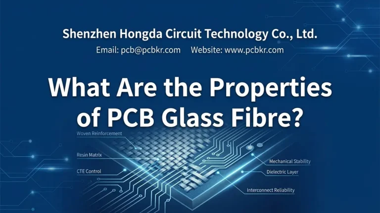
    Posted in PCB Design, Material Engineering, High‑Speed PCB | Reading time: 12 minutes Blog Excerpt: PCB glass fibre is far more than simple filler material. This engineering guide breaks down how glass‑fibre properties define PCB mechanical stiffness, thermal reliability, plated‑through‑hole lifetime and high‑speed signal integrity for automotive, industrial and high‑reliability hardware projects. Table of Contents…
    Read More What Are the Properties of PCB Glass Fibre? Engineering GuideContinue

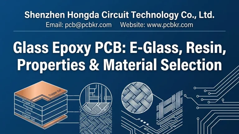
  • Glass epoxy PCB material layers and properties guide by Hongda Circuit
    Blog

    Glass Epoxy PCB: E-Glass, Resin, Properties & Material Selection

    ByDavid 09/09/202609/11/2026

    Glass epoxy PCB uses woven glass fiber reinforcement combined with an epoxy resin system and copper foil to create a mechanically stable, electrically insulating circuit‑board laminate. The actual performance of a glass epoxy PCB depends not only on whether it is classified as FR‑4, but also on glass style, resin content, Tg, CTE, Dk, Df,…

    Read More Glass Epoxy PCB: E-Glass, Resin, Properties & Material SelectionContinue

  • Shenzhen Hongda Circuit Technology Glass PCB Materials Types Manufacturing and Supplier Selection Guide
    Blog

    Glass PCB: Materials, Types, Manufacturing & Supplier Selection

    ByDavid 09/08/202609/11/2026

    Glass PCB can refer to either a conventional glass‑fiber‑reinforced PCB, such as FR‑4 and high‑Tg laminates, or an emerging glass‑substrate/glass‑core circuit architecture using TGVs. Choosing the right structure depends on electrical performance, dimensional stability, thermal reliability, interconnect density, manufacturing capability, and production volume. Table of Contents What Is a Glass PCB? A Glass PCB is…

    Read More Glass PCB: Materials, Types, Manufacturing & Supplier SelectionContinue

  • Embedded Component PCB Lead Time Manufacturing & Procurement Guide by Shenzhen Hongda Circuit Technology Co., Ltd. featuring PCB circuit board graphics, components, and contact info pcb@pcbkr.com
    Blog

    Embedded Component PCB Lead Time: Manufacturing & Procurement Guide

    ByDavid 09/08/202609/11/2026

    Embedded Component PCB lead time is typically 10–20 working days for standard builds and about 15–30+ working days for complex HDI, mSAP, specialty‑material, or multi‑lamination designs. Expedited production may reach 7–10 working days when engineering files, materials, components, capacity, and testing requirements are ready. For procurement engineers, however, the quoted number is only part of…

    Read More Embedded Component PCB Lead Time: Manufacturing & Procurement GuideContinue

  • Embedded Component PCB Price Guide and Cost Factors Banner - Shenzhen Hongda Circuit Technology Co., Ltd.
    Blog

    Embedded Component PCB Price: Cost Factors, Pricing, and Cost Reduction

    ByDavid 09/08/202609/11/2026

    Embedded Component PCB Price depends on far more than simple board dimensions and layer quantity. Multiple critical factors drive final costs, including embedded component type, cavity design complexity, component Z‑height requirements, HDI build structures, repeated lamination cycles, base material selection, specialized inspection procedures, custom tooling, production volume, and expected manufacturing yield. To build reliable project…

    Read More Embedded Component PCB Price: Cost Factors, Pricing, and Cost ReductionContinue

  • Embedded Component PCB Cost, Pricing, Cost Breakdown and Optimization guide by Shenzhen Hongda Circuit Technology Co., Ltd.
    Blog

    Embedded Component PCB Cost: Pricing, Cost Breakdown & Optimization

    ByDavid 09/08/202609/11/2026

    Embedded Component PCB cost depends mainly on component type, layer count, cavity complexity, HDI structure, materials, testing, production yield, tooling, and volume. A useful early budget is typically tens to several hundred US dollars per prototype board, while high‑volume production can reduce unit cost substantially. The important question is not simply “How much does an embedded…

    Read More Embedded Component PCB Cost: Pricing, Cost Breakdown & OptimizationContinue

  • Shenzhen Hongda Circuit Technology Co., Ltd. Consumer Electronics Embedded Component PCB: Design, Manufacturing & Procurement Guide
    Blog

    Consumer Electronics Embedded Component PCB: Design, Manufacturing & Procurement Guide

    ByDavid 09/07/202609/11/2026

    Consumer electronics manufacturers are under constant pressure to put more functions into smaller products. Embedded Component PCB technology helps recover PCB surface area, shorten selected interconnects and increase functional density by integrating passive or active components inside the PCB structure. For smartphones, wearables, TWS earbuds, AR/VR devices and compact IoT products, however, successful implementation depends…

    Read More Consumer Electronics Embedded Component PCB: Design, Manufacturing & Procurement GuideContinue

  • High-Density Embedded Component PCB manufacturing with HDI, mSAP and cavity control
    Blog

    High-Density Embedded Component PCB: Engineering and Procurement Guide

    ByDavid 09/07/202609/11/2026

    A focused cluster page for engineers, OEM buyers, and sourcing teams evaluating embedded component PCB manufacturing—not a general PCB technology overview. What is the manufacturing definition of a high-density embedded component PCB? It is a multilayer PCB in which selected passive devices, packaged active devices, or bare dies are formed or placed inside the board…

    Read More High-Density Embedded Component PCB: Engineering and Procurement GuideContinue

  • High-Frequency Embedded Component PCB stack-up and manufacturing guide by Shenzhen Hongda Circuit
    Blog

    High-Frequency Embedded PCB Manufacturer | Prototype to Volume

    ByDavid 09/07/202609/11/2026

    High-Frequency Embedded Component PCB is a specialized circuit board solution that integrates embedded capacitors, resistors, inductors and other passive components as well as active devices, while adopting low-loss dielectric materials, controlled impedance design, microvia technology and precision lamination processes for high-frequency signal scenarios. Different from conventional miniaturized PCB fabrication that merely regards component embedding as…

    Read More High-Frequency Embedded PCB Manufacturer | Prototype to VolumeContinue

  • Industrial IoT embedded component PCB sample with microvias and thermal design by Hongda Circuit.
    Blog

    Industrial IoT Embedded Component PCB Guide: DFM, Cavity Fabrication & Reliability Qualification

    ByDavid 09/07/202609/11/2026

    Industrial IoT embedded component PCBs integrate selected passive or active devices inside the multilayer board to increase functional density, recover surface area, shorten critical interconnects, and improve packaging efficiency. They are especially useful for compact industrial sensors, remote I/O, PLC modules, edge controllers, gateways, and condition‑monitoring equipment. Industrial IoT equipment creates a difficult PCB design…

    Read More Industrial IoT Embedded Component PCB Guide: DFM, Cavity Fabrication & Reliability QualificationContinue

Page navigation

Previous PagePrevious 1 … 13 14 15 16 17 … 44 Next PageNext

Shenzhen Hongda Circuit Technology Co., Ltd

Address: Room 1608-1610, Research Development Comprehensive Building, Baoyunda Logistics Center, Baoan, Shenzhen, China

E-mail:sales@pcbkr.com

TEL:+86 0755 23720053

Industry Insight Blog

PCB manufacturer

High-Frequency PCB

HDI PCB

Multilayer PCB

Metal Core PCB

High-Speed PCB

Heavy Copper PCB

Flex PCB

Rigid-Flex PCB

IC Substrates PCB

Technology

120-Layer 5G-Advanced/6G Communication Boards

High-Speed Semiconductor Test Boards

mSAP-Processed IC Package Substrates

Specialized Millimeter-Wave Radar PCBs

224Gbps High-Frequency Microwave Circuits

Intelligent Industrial Control PCBs

© 2026 Shenzhen Hongda Circuit Technology Co., Ltd.

  • Home
  • PCB Products
    • High-Frequency PCB
    • HDI PCB
    • Multilayer PCB
    • Metal Core PCB
    • High-Speed PCB
    • Heavy Copper PCB
    • Flex PCB
    • Rigid-Flex PCB
    • IC Substrates PCB
  • PCB Assembly
    •  Advanced BGA & SMT 
    • Box Build & Cable Assy 
    • Component Sourcing
    • Turnkey & Consignment
  • Capability Overview
    • Capability
    • Advanced Equipment
    • PCB Design & Eng.
    • Standard PCB Capability
    • IC Substrate Capability
    • HDI PCB Capability
    • Rigid-Flex Capability
    • RF PCB Capability
    • High frequency PCBs Capability
  • Technology
    • 120-Layer 5G-Advanced/6G Communication Boards
    • High-Speed Semiconductor Test Boards
    • mSAP-Processed IC Package Substrates
    • Specialized Millimeter-Wave Radar PCBs
    • 224Gbps High-Frequency Microwave Circuits
    • Intelligent Industrial Control PCBs
    • FAQ
  • Blog
  • About Us
    • Certifications
  • Contact