Skip to content
PCBkr.com
  • Home
  • PCB ProductsExpand
    • High-Frequency PCB
    • HDI PCB
    • Multilayer PCB
    • Metal Core PCB
    • High-Speed PCB
    • Heavy Copper PCB
    • Flex PCB
    • Rigid-Flex PCB
    • IC Substrates PCB
  • PCB AssemblyExpand
    •  Advanced BGA & SMT 
    • Box Build & Cable Assy 
    • Component Sourcing
    • Turnkey & Consignment
  • Capability OverviewExpand
    • Capability
    • Advanced Equipment
    • PCB Design & Eng.
    • Standard PCB Capability
    • IC Substrate Capability
    • HDI PCB Capability
    • Rigid-Flex Capability
    • RF PCB Capability
    • High frequency PCBs Capability
  • TechnologyExpand
    • 120-Layer 5G-Advanced/6G Communication Boards
    • High-Speed Semiconductor Test Boards
    • mSAP-Processed IC Package Substrates
    • Specialized Millimeter-Wave Radar PCBs
    • 224Gbps High-Frequency Microwave Circuits
    • Intelligent Industrial Control PCBs
    • FAQ
  • Blog
  • About UsExpand
    • Certifications
  • Contact
  • EV Embedded Component PCB Engineering and Procurement Guide by Shenzhen Hongda Circuit Technology
    Blog

    EV Embedded Component PCB: Key Considerations for EV Engineers and Procurement Teams

    ByDavid 09/04/202609/11/2026

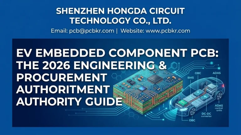
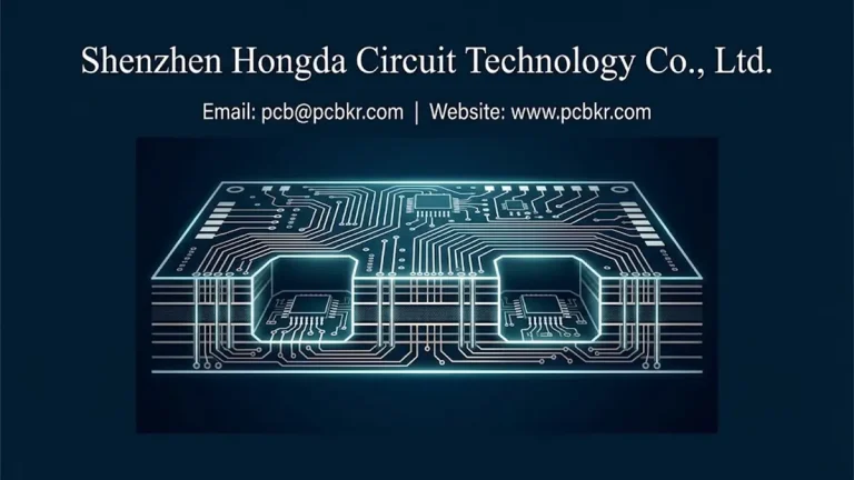
    What Is an EV Embedded Component PCB? An EV embedded component PCB integrates selected electronic components—resistors, capacitors, inductors, and even active dies—inside the multilayer board structure rather than mounting them exclusively on the surface. For electric vehicles, this is not simply a miniaturization tactic. It is a systems-integration strategy that combines circuitry, components, interconnections, and…
    Read More EV Embedded Component PCB: Key Considerations for EV Engineers and Procurement TeamsContinue

  • Automotive Embedded Component PCB Guide Header Image by Shenzhen Hongda Circuit Technology Co., Ltd.
    Blog

    Automotive Embedded Component PCB Guide

    ByDavid 09/04/202609/11/2026

    Chapter 1: Embedded Component Technology Roadmap — Three Implementation Methods SOLDER.embedding PCB Technology Cross-Section Diagram Automotive Embedded Component PCB manufacturing varies drastically across manufacturers in process standards and structural design. For automotive procurement and engineering teams, the selection of a proper component embedding topology is a core decisive factor for designs to pass ISO 26262…

    Read More Automotive Embedded Component PCB GuideContinue

  • Embedded Component PCB IPC Standards Guide by Hongda Circuit
    Blog

    Embedded Component PCB IPC Standards: A Manufacturing and Procurement Guide

    ByDavid 09/04/202609/11/2026

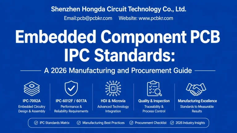
    Embedded Component PCB IPC Standards, primarily guided by IPC-7092A for design and process implementation, require pairing with performance specifications such as IPC-6017A and IPC-6012F based on the board’s embedded structure, HDI construction, materials, assembly process, product class, and reliability demands. Rather than simply claiming “IPC compliant,” a reliable supplier converts these standards into measurable fabrication,…

    Read More Embedded Component PCB IPC Standards: A Manufacturing and Procurement GuideContinue

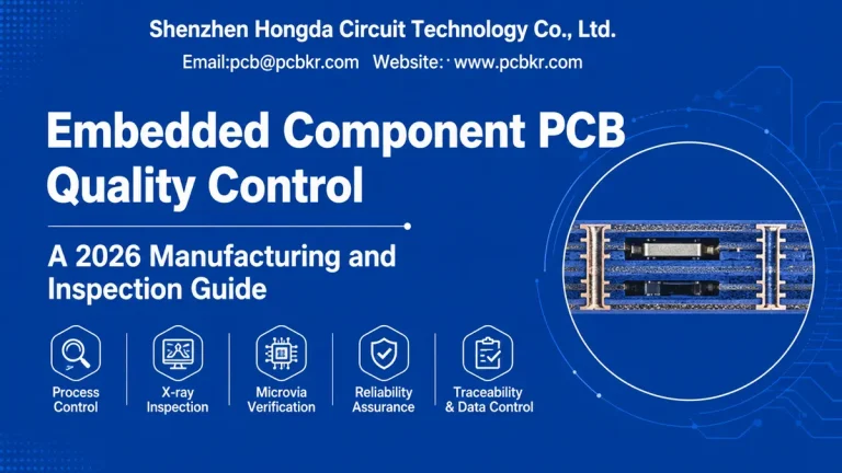
  • Embedded component PCB quality control guide 2026 by Shenzhen Hongda Circuit Technology showing microsection analysis and inspection workflow
    Blog

    Embedded Component PCB Quality Control: An Advanced Manufacturing and Inspection Guide

    ByDavid 09/04/202609/11/2026

    Embedded component PCB quality control requires process‑level control from material receiving through component placement, cavity machining, lamination, laser microvia formation, plating, inspection, electrical testing, and lot traceability. The critical difference is that many internal defects become inaccessible after lamination, so manufacturers must verify hidden structures before they are permanently sealed. For Shenzhen Hongda Circuit Technology…

    Read More Embedded Component PCB Quality Control: An Advanced Manufacturing and Inspection GuideContinue

  • Embedded Component PCB Reliability, Failure Modes and 2026 Manufacturing Controls Cover - Shenzhen Hongda Circuit Technology Co., Ltd.
    Blog

    Embedded Component PCB Reliability: Failure Modes, Validation and Manufacturing Controls

    ByDavid 09/04/202609/11/2026

    Embedded component PCB reliability is controlled by the complete embedded structure—not the component alone. reliable production requires coordinated cavity geometry, CTE-aware materials, controlled lamination, laser microvias, copper interface quality, electrical monitoring, cross-section analysis and application-specific thermal-mechanical validation. This article expands the original reliability framework into a manufacturing-oriented guide for engineers, OEMs, EMS companies and PCB…

    Read More Embedded Component PCB Reliability: Failure Modes, Validation and Manufacturing ControlsContinue

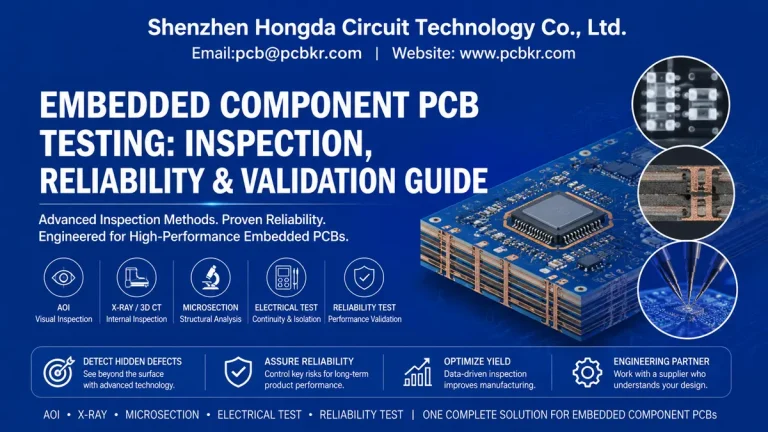
  • Embedded Component PCB Testing: Inspection, Reliability, and Validation Guide by Shenzhen Hongda
    Blog

    Embedded Component PCB Testing: Inspection, Reliability and Validation Guide

    ByDavid 09/03/202609/11/2026

    Embedded component PCB testing requires a layered inspection strategy combining AOI, 2D/3D X‑ray, microsection analysis, dimensional measurement, electrical testing and reliability validation. Because embedded components, microvias, buried connections and internal solder structures are inaccessible after lamination, no single inspection method can adequately validate the finished PCB. For manufacturers and buyers of embedded component PCBs, the…

    Read More Embedded Component PCB Testing: Inspection, Reliability and Validation GuideContinue

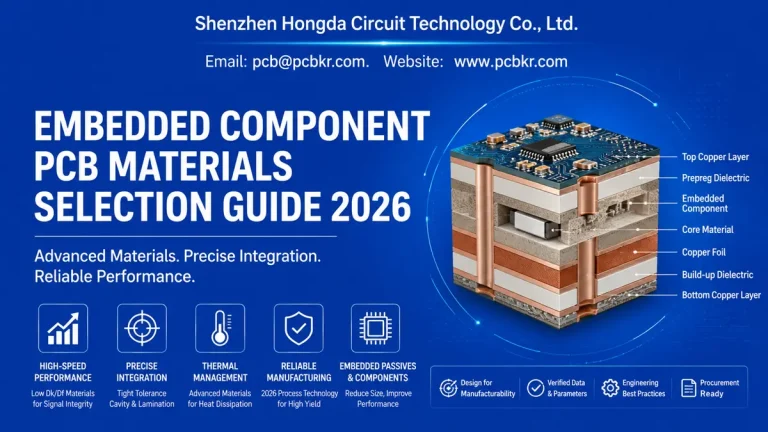
  • Embedded component PCB materials selection guide 2026 and 3D stackup structure by Shenzhen Hongda Circuit Technology Co., Ltd.
    Blog

    Embedded Component PCB Materials: 2026 Selection Guide for High-Density PCB Manufacturing

    ByDavid 09/03/202609/11/2026

    Embedded component PCB materials must be selected as a complete electrical, mechanical and manufacturing system—not as a laminate brand alone. For 2026 designs, the decision should link dielectric Dk/Df, copper roughness, resin flow, cavity geometry, CTE, thermal performance, component compatibility, and measurable impedance or reliability targets to the actual stack-up. This revised guide expands the…

    Read More Embedded Component PCB Materials: 2026 Selection Guide for High-Density PCB ManufacturingContinue

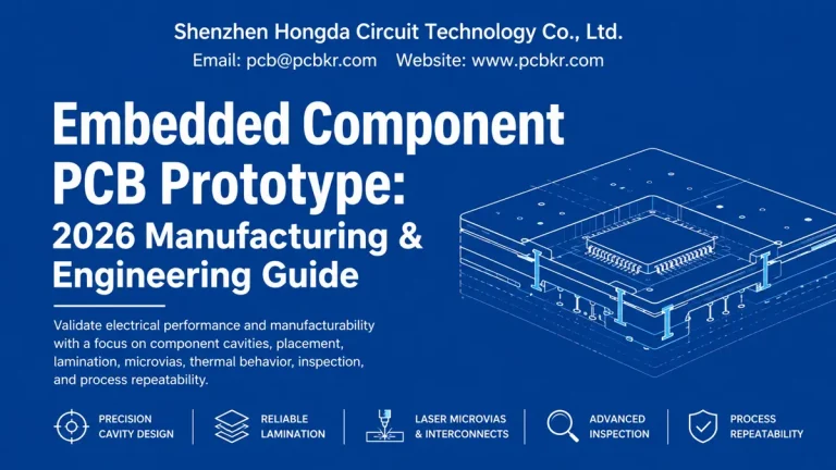
  • Infographic for Embedded Component PCB Prototype guide featuring 3D multilayer structure and key manufacturing parameters by Shenzhen Hongda
    Blog

    Embedded Component PCB Prototype: From Design Validation to Production

    ByDavid 09/03/202609/11/2026

    An embedded component PCB prototype validates both electrical performance and manufacturability before mass production, with special attention to component cavities, placement, lamination, microvias, thermal behavior, inspection, and process repeatability. What Is an Embedded Component PCB Prototype? 3D representation of an embedded component PCB prototype featuring a dedicated internal cavity, laminated substrate layers, and high-density interconnect…

    Read More Embedded Component PCB Prototype: From Design Validation to ProductionContinue

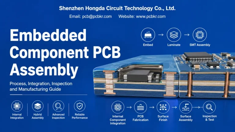
  • Embedded component PCB assembly process cross-section showing internal component integration and conventional surface SMT assembly by Hongda Circuit
    Blog

    Embedded Component PCB Assembly: Engineering and Manufacturing Guide

    ByDavid 09/03/202609/11/2026

    Embedded component PCB assembly differs from conventional SMT assembly because some components are integrated into the PCB before conventional surface assembly begins. The manufacturing challenge is coordinating internal component integration with the subsequent outer-layer SMT process. What Is Embedded Component PCB Assembly? Embedded component PCB assembly is the process of integrating selected electronic components into…

    Read More Embedded Component PCB Assembly: Engineering and Manufacturing GuideContinue

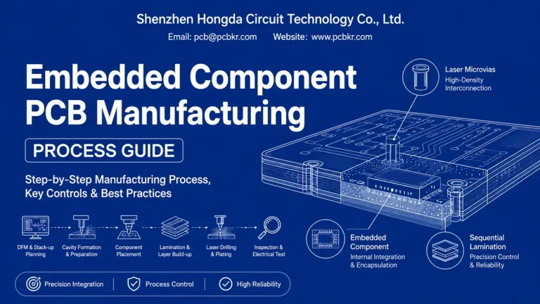
  • Embedded component PCB manufacturing process guide illustrating cavity formation, component placement, sequential lamination, and laser microvias by Hongda Circuit.
    Blog

    Embedded Component PCB Manufacturing Process: Step-by-Step Guide

    ByDavid 09/03/202609/11/2026

    An embedded component PCB requires a controlled manufacturing sequence that integrates component placement with PCB fabrication. The critical process stages include inner-layer preparation, cavity formation, component placement, lamination, laser drilling, plating, routing, surface finishing, inspection and electrical verification. Unlike a conventional multilayer PCB, embedded-component fabrication cannot treat PCB fabrication and component integration as independent operations….

    Read More Embedded Component PCB Manufacturing Process: Step-by-Step GuideContinue

Page navigation

Previous PagePrevious 1 … 14 15 16 17 18 … 44 Next PageNext

Shenzhen Hongda Circuit Technology Co., Ltd

Address: Room 1608-1610, Research Development Comprehensive Building, Baoyunda Logistics Center, Baoan, Shenzhen, China

E-mail:sales@pcbkr.com

TEL:+86 0755 23720053

Industry Insight Blog

PCB manufacturer

High-Frequency PCB

HDI PCB

Multilayer PCB

Metal Core PCB

High-Speed PCB

Heavy Copper PCB

Flex PCB

Rigid-Flex PCB

IC Substrates PCB

Technology

120-Layer 5G-Advanced/6G Communication Boards

High-Speed Semiconductor Test Boards

mSAP-Processed IC Package Substrates

Specialized Millimeter-Wave Radar PCBs

224Gbps High-Frequency Microwave Circuits

Intelligent Industrial Control PCBs

© 2026 Shenzhen Hongda Circuit Technology Co., Ltd.

  • Home
  • PCB Products
    • High-Frequency PCB
    • HDI PCB
    • Multilayer PCB
    • Metal Core PCB
    • High-Speed PCB
    • Heavy Copper PCB
    • Flex PCB
    • Rigid-Flex PCB
    • IC Substrates PCB
  • PCB Assembly
    •  Advanced BGA & SMT 
    • Box Build & Cable Assy 
    • Component Sourcing
    • Turnkey & Consignment
  • Capability Overview
    • Capability
    • Advanced Equipment
    • PCB Design & Eng.
    • Standard PCB Capability
    • IC Substrate Capability
    • HDI PCB Capability
    • Rigid-Flex Capability
    • RF PCB Capability
    • High frequency PCBs Capability
  • Technology
    • 120-Layer 5G-Advanced/6G Communication Boards
    • High-Speed Semiconductor Test Boards
    • mSAP-Processed IC Package Substrates
    • Specialized Millimeter-Wave Radar PCBs
    • 224Gbps High-Frequency Microwave Circuits
    • Intelligent Industrial Control PCBs
    • FAQ
  • Blog
  • About Us
    • Certifications
  • Contact