Skip to content
PCBkr.com
  • Home
  • PCB ProductsExpand
    • High-Frequency PCB
    • HDI PCB
    • Multilayer PCB
    • Metal Core PCB
    • High-Speed PCB
    • Heavy Copper PCB
    • Flex PCB
    • Rigid-Flex PCB
    • IC Substrates PCB
  • PCB AssemblyExpand
    •  Advanced BGA & SMT 
    • Box Build & Cable Assy 
    • Component Sourcing
    • Turnkey & Consignment
  • Capability OverviewExpand
    • Capability
    • Advanced Equipment
    • PCB Design & Eng.
    • Standard PCB Capability
    • IC Substrate Capability
    • HDI PCB Capability
    • Rigid-Flex Capability
    • RF PCB Capability
    • High frequency PCBs Capability
  • TechnologyExpand
    • 120-Layer 5G-Advanced/6G Communication Boards
    • High-Speed Semiconductor Test Boards
    • mSAP-Processed IC Package Substrates
    • Specialized Millimeter-Wave Radar PCBs
    • 224Gbps High-Frequency Microwave Circuits
    • Intelligent Industrial Control PCBs
    • FAQ
  • Blog
  • About UsExpand
    • Certifications
  • Contact
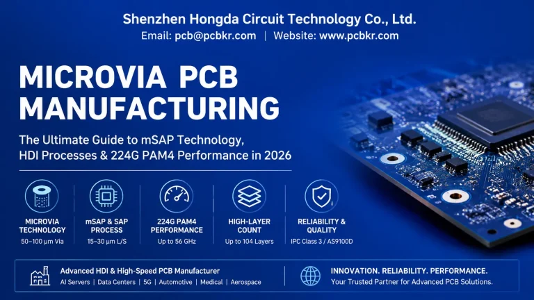
  • Shenzhen Hongda Circuit Technology (PCBKR) Microvia PCB Manufacturing Capabilities: mSAP & SAP processes, 224G PAM4 performance, high-layer count up to 104, for AI servers, data centers, and aerospace.
    Blog

    High-Density Interconnect (HDI) Microvia PCB Manufacturing | mSAP & SAP Capabilities for AI Server and HPC Applications

    ByDavid 08/05/202608/07/2026

    Introduction: Why Microvia PCB Technology Defines the Next Generation of Interconnects The global electronics industry is undergoing a structural transformation. AI server clusters, 5G-Advanced base stations, autonomous driving compute platforms, and high-performance computing (HPC) accelerators are pushing printed circuit board (PCB) technology into territories once reserved for semiconductor packaging. At the center of this shift…
    Read More High-Density Interconnect (HDI) Microvia PCB Manufacturing | mSAP & SAP Capabilities for AI Server and HPC ApplicationsContinue

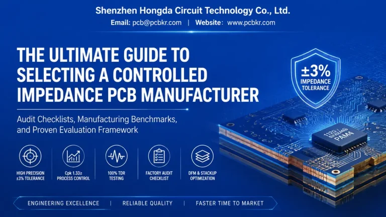
  • The ultimate guide to selecting a controlled impedance PCB manufacturer featuring Cpk >= 1.33 process control, +-3% tolerance, and 100% TDR testing by Shenzhen Hongda Circuit Technology.
    Blog

    Controlled Impedance PCB Manufacturer: Fabrication, TDR Testing & Quality Control

    ByDavid 08/04/202611/16/2026

    Selecting a controlled impedance PCB manufacturer requires more than finding a factory that can produce 50Ω or 100Ω traces. OEM buyers must verify whether the manufacturer can translate electrical requirements into a manufacturable stackup, control critical fabrication variables, and provide appropriate measurement evidence for the finished boards. Shenzhen Hongda Circuit Technology Co., Ltd. manufactures precision…

    Read More Controlled Impedance PCB Manufacturer: Fabrication, TDR Testing & Quality ControlContinue

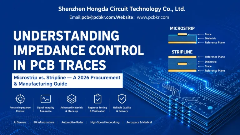
  • How to achieve controlled impedance in PCB design: Microstrip vs Stripline stackup diagram by Shenzhen Hongda Circuit
    Blog

    Understanding Impedance Control in PCB Traces: Microstrip vs. Stripline — A Procurement & Manufacturing Guide

    ByDavid 08/03/202608/04/2026

    How to achieve controlled impedence in pcb is a critical technical question that cannot be overlooked when sourcing printed circuit boards for high-end scenarios including AI servers, 5G infrastructure, and automotive radar modules. Unlike conventional low-frequency circuit designs, a PCB trace in 2026’s high-speed electronic systems is no longer a simple copper conductor for current…

    Read More Understanding Impedance Control in PCB Traces: Microstrip vs. Stripline — A Procurement & Manufacturing GuideContinue

  • PCB impedance control service showing high-speed microstrip trace cross-section with W, H, T, Dk parameters and TDR impedance calculations.
    Blog

    PCB Trace Impedance Control 101: From Theory to Layout Practice

    ByDavid 08/03/202608/04/2026

    1. Introduction: Why Impedance Control Is a Must for High-Speed PCBs PCB Impedance Control Service has become a fundamental requirement in modern high-speed electronics manufacturing, where trace design directly dictates signal integrity. In early low-speed circuits, a PCB trace was viewed simply as a “copper wire,” with engineers focusing almost entirely on current conductivity and…

    Read More PCB Trace Impedance Control 101: From Theory to Layout PracticeContinue

  • What is impedance control in PCB guide showing 3D stackup layers, TDR testing, and manufacturing specs by Hongda Circuit
    Blog

    What Is Impedance Control in PCB? A Complete Procurement & Engineering Guide

    ByDavid 08/03/202608/04/2026

    3D Cross-Section of Controlled Impedance PCB Stackup – PCBkr Introduction: When the Formula Betrays You Your signal-integrity engineer spent three weeks in Polar Si9000. The stackup checks out: 50 Ω single-ended, 100 Ω differential, Megtron 7 core, everything within ±10 % on paper. You send the RFQ to three factories. The lowest bidder wins. Fourteen…

    Read More What Is Impedance Control in PCB? A Complete Procurement & Engineering GuideContinue

  • The Ultimate Procurement Guide to Impedance Controlled PCBs - Hongda Circuit
    Blog

    The Ultimate Procurement Guide to Impedance Controlled PCBs: From Stackup Engineering to Supplier Qualification for 224G PAM4 and AI Server Applications

    ByDavid 08/03/202608/04/2026

    An impedance controlled PCB is a precision-engineered circuit board where trace geometry, dielectric materials, and manufacturing tolerances are tightly regulated to maintain consistent electrical impedance—typically 50Ω single-ended or 90Ω/100Ω differential—across high-speed signal paths. For procurement teams sourcing boards for 5G infrastructure, AI accelerators, or automotive radar, selecting the right controlled impedance PCB manufacturer determines whether…

    Read More The Ultimate Procurement Guide to Impedance Controlled PCBs: From Stackup Engineering to Supplier Qualification for 224G PAM4 and AI Server ApplicationsContinue

  • Hard gold PCB manufacturer producing Class 3 edge connector boards with selective gold plating
    Blog

    Sourcing Hard Gold PCBs in Bulk: A Procurement Director’s Guide to China OEM Manufacturing

    ByDavid 07/31/202608/04/2026

    Hard gold PCB manufacturer selection stands as a critical yet often overlooked factor in server hardware reliability, directly impacting the long-term operational stability of core equipment. Many server backplane failures occurring after 500 insertion cycles stem from underspecified edge connector finishes, a subtle quality flaw that rarely lands immediate blame on the procurement team. Nevertheless,…

    Read More Sourcing Hard Gold PCBs in Bulk: A Procurement Director’s Guide to China OEM ManufacturingContinue

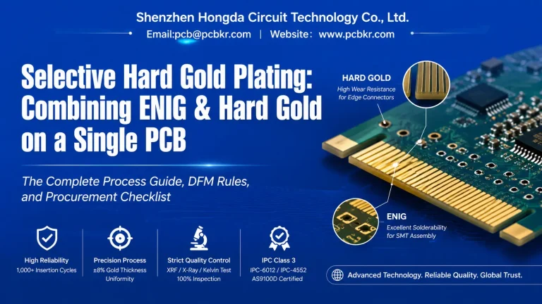
  • Selective hard gold PCB showing ENIG on SMT pads and electroplated hard gold on edge connectors for high wear resistance.
    Blog

    Selective Hard Gold Plating: Combining ENIG & Hard Gold on a Single PCB

    ByDavid 07/31/202608/04/2026

    Why Selective Hard Gold? Solving the SMT Solderability vs. Edge Connector Wear Resistance Dilemma Dual Surface Finish PCB: ENIG BGA Pads & Hard Gold Edge Connectors Modern PCB designs rarely demand a single surface finish across the entire board. A typical high-reliability board—whether an AI server accelerator card, a military VPX backplane, or an automotive…

    Read More Selective Hard Gold Plating: Combining ENIG & Hard Gold on a Single PCBContinue

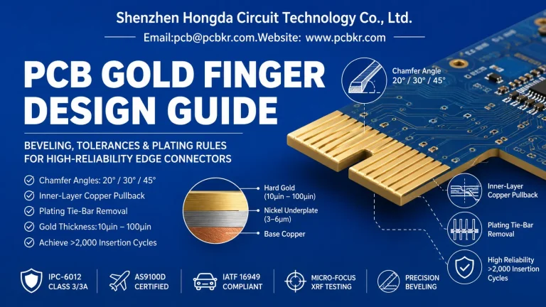
  • PCB gold finger design guide showing 20 30 45 degree beveling angles, hard gold plating stackup, and inner layer pullback rules.
    Blog

    PCB Gold Finger Design Guide: Beveling, Tolerances & Plating Rules for High-Reliability Edge Connectors

    ByDavid 07/31/202608/04/2026

    PCB Gold Finger serves as the core conductive and mechanical contact component of printed circuit board edge connectors, acting as the definitive electrical and mechanical bridge that links a daughter card to its host system in hardware design. In the engineering specification workflow of hardware engineers, the design and validation of PCB gold fingers are…

    Read More PCB Gold Finger Design Guide: Beveling, Tolerances & Plating Rules for High-Reliability Edge ConnectorsContinue

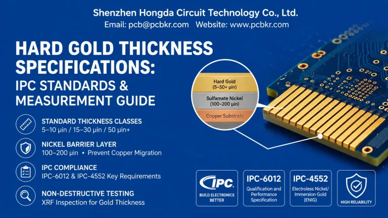
  • Hard gold thickness PCB specifications diagram showing gold finger layer structure, IPC-6012 standards, and XRF measurement guide by Hongda Circuit.
    Blog

    Hard Gold Thickness Specifications: IPC Standards & Measurement Guide for Procurement Engineers

    ByDavid 07/31/202608/04/2026

    Hard gold thickness PCB parameters are decisive to the field reliability of gold finger edge connectors. When a gold finger edge connector fails in the field, the repair cost typically exceeds the entire PCB fabrication budget by an order of magnitude. Procurement teams have learned this the hard way: a 30 µin hard gold specification…

    Read More Hard Gold Thickness Specifications: IPC Standards & Measurement Guide for Procurement EngineersContinue

Page navigation

Previous PagePrevious 1 … 23 24 25 26 27 … 44 Next PageNext

Shenzhen Hongda Circuit Technology Co., Ltd

Address: Room 1608-1610, Research Development Comprehensive Building, Baoyunda Logistics Center, Baoan, Shenzhen, China

E-mail:sales@pcbkr.com

TEL:+86 0755 23720053

Industry Insight Blog

PCB manufacturer

High-Frequency PCB

HDI PCB

Multilayer PCB

Metal Core PCB

High-Speed PCB

Heavy Copper PCB

Flex PCB

Rigid-Flex PCB

IC Substrates PCB

Technology

120-Layer 5G-Advanced/6G Communication Boards

High-Speed Semiconductor Test Boards

mSAP-Processed IC Package Substrates

Specialized Millimeter-Wave Radar PCBs

224Gbps High-Frequency Microwave Circuits

Intelligent Industrial Control PCBs

© 2026 Shenzhen Hongda Circuit Technology Co., Ltd.

  • Home
  • PCB Products
    • High-Frequency PCB
    • HDI PCB
    • Multilayer PCB
    • Metal Core PCB
    • High-Speed PCB
    • Heavy Copper PCB
    • Flex PCB
    • Rigid-Flex PCB
    • IC Substrates PCB
  • PCB Assembly
    •  Advanced BGA & SMT 
    • Box Build & Cable Assy 
    • Component Sourcing
    • Turnkey & Consignment
  • Capability Overview
    • Capability
    • Advanced Equipment
    • PCB Design & Eng.
    • Standard PCB Capability
    • IC Substrate Capability
    • HDI PCB Capability
    • Rigid-Flex Capability
    • RF PCB Capability
    • High frequency PCBs Capability
  • Technology
    • 120-Layer 5G-Advanced/6G Communication Boards
    • High-Speed Semiconductor Test Boards
    • mSAP-Processed IC Package Substrates
    • Specialized Millimeter-Wave Radar PCBs
    • 224Gbps High-Frequency Microwave Circuits
    • Intelligent Industrial Control PCBs
    • FAQ
  • Blog
  • About Us
    • Certifications
  • Contact