Skip to content
PCBkr.com
  • Home
  • PCB ProductsExpand
    • High-Frequency PCB
    • HDI PCB
    • Multilayer PCB
    • Metal Core PCB
    • High-Speed PCB
    • Heavy Copper PCB
    • Flex PCB
    • Rigid-Flex PCB
    • IC Substrates PCB
  • PCB AssemblyExpand
    •  Advanced BGA & SMT 
    • Box Build & Cable Assy 
    • Component Sourcing
    • Turnkey & Consignment
  • Capability OverviewExpand
    • Capability
    • Advanced Equipment
    • PCB Design & Eng.
    • Standard PCB Capability
    • IC Substrate Capability
    • HDI PCB Capability
    • Rigid-Flex Capability
    • RF PCB Capability
    • High frequency PCBs Capability
  • TechnologyExpand
    • 120-Layer 5G-Advanced/6G Communication Boards
    • High-Speed Semiconductor Test Boards
    • mSAP-Processed IC Package Substrates
    • Specialized Millimeter-Wave Radar PCBs
    • 224Gbps High-Frequency Microwave Circuits
    • Intelligent Industrial Control PCBs
    • FAQ
  • Blog
  • About UsExpand
    • Certifications
  • Contact
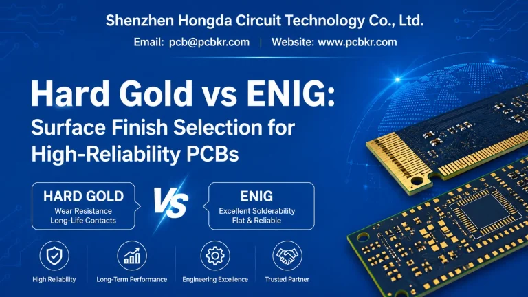
  • Banner image for Hard Gold vs ENIG PCB surface finish comparison guide by Shenzhen Hongda Circuit, featuring gold finger edge connectors and ENIG SMT pads.
    Blog

    Hard Gold vs ENIG: Surface Finish Selection for High-Reliability PCBs

    ByDavid 07/30/202610/13/2026

    Why Surface Finish Selection Determines Product Lifecycle Costs A PCB surface finish does more than prevent copper oxidation. It defines solder joint reliability, contact resistance stability, and mechanical durability across the product’s entire service life. Choose incorrectly, and you risk field failures ranging from BGA voiding to edge connector fretting corrosion. Choose correctly, and you…
    Read More Hard Gold vs ENIG: Surface Finish Selection for High-Reliability PCBsContinue

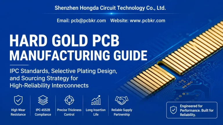
  • Hard Gold PCB Manufacturing Guide cover image by Shenzhen Hongda Circuit, highlighting IPC-4552B standards and selective plating.
    Blog

    Hard Gold PCB Manufacturing & Plating Guide: IPC Standards, Selective Plating Design, and Sourcing Strategy for High-Reliability Interconnects

    ByDavid 07/30/202608/04/2026

    What Is Hard Gold PCB and How Does It Differ from ENIG? 1.1: Defining Electroplated Hard Gold on PCBs When hardware engineers specify a Hard Gold PCB, they are referring to an electrolytically deposited gold-nickel alloy coating—typically hardened with cobalt or nickel additives—applied over an electrolytic nickel underlayer. Unlike the soft, immersion-deposited gold used in…

    Read More Hard Gold PCB Manufacturing & Plating Guide: IPC Standards, Selective Plating Design, and Sourcing Strategy for High-Reliability InterconnectsContinue

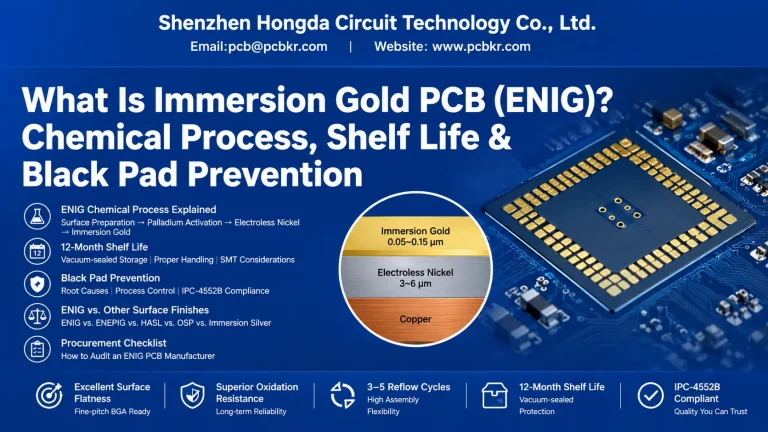
  • What Is Immersion Gold PCB (ENIG) chemical process, layer structure, and black pad prevention guide by Hongda Circuit
    Blog

    What Is Immersion Gold PCB (ENIG)? Chemical Process, Shelf Life & Black Pad Prevention

    ByDavid 07/29/202610/13/2026

    Quick Engineering Definition: ENIG (Electroless Nickel Immersion Gold) is a dual-layer metallic surface finish for printed circuit boards, consisting of 3–6 µm of electroless nickel-phosphorus alloy capped by 0.05–0.15 µm of immersion gold. It delivers exceptional surface flatness for fine-pitch QFP and BGA assembly, superior oxidation resistance, and a 12-month shelf life under vacuum-sealed storage….

    Read More What Is Immersion Gold PCB (ENIG)? Chemical Process, Shelf Life & Black Pad PreventionContinue

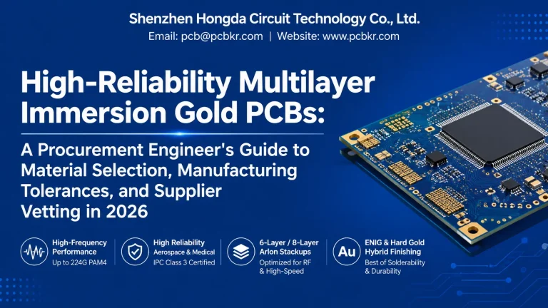
  • High-Reliability Multilayer Immersion Gold PCB Guide by Shenzhen Hongda Circuit Technology
    Blog

    High Reliability Multilayer Immersion Gold PCBs: A Procurement Engineer’s Guide to Material Selection, Manufacturing Tolerances, and Supplier Vetting

    ByDavid 07/29/202608/04/2026

    Executive Summary: Why Immersion Gold PCB Procurement Decisions Matter More The global PCB ENIG chemical market has crossed USD 3.5 billion in China alone and is accelerating toward USD 5.0 billion by 2033 at a 6.2% CAGR, driven by 5G infrastructure, electric vehicles, and AI server hardware demanding sub-micron plating precision. For procurement leads and…

    Read More High Reliability Multilayer Immersion Gold PCBs: A Procurement Engineer’s Guide to Material Selection, Manufacturing Tolerances, and Supplier VettingContinue

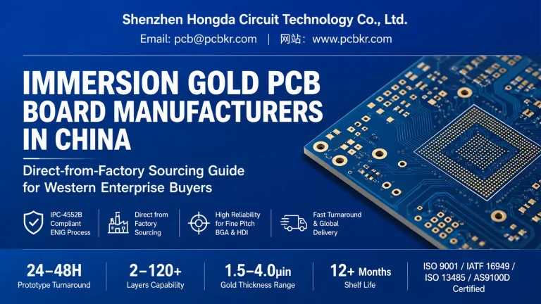
  • Immersion Gold PCB Board Manufacturers in China - Direct Sourcing Guide Banner by Shenzhen Hongda Circuit Technology
    Blog

    Immersion Gold PCB Board Manufacturers in China: Direct-from-Factory Sourcing Guide for Western Enterprise Buyers

    ByDavid 07/29/202608/04/2026

    Executive Summary: Standard ENIG Specifications at a Glance For procurement engineers vetting immersion gold PCB board manufacturers in China, the first gate is verifying that the factory holds its electroless nickel immersion gold (ENIG) process within the IPC-4552B process window. The table below summarizes the non-negotiable parameters every Western buyer should demand on the fabrication…

    Read More Immersion Gold PCB Board Manufacturers in China: Direct-from-Factory Sourcing Guide for Western Enterprise BuyersContinue

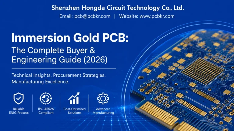
  • Immersion Gold PCB: The Complete Buyer & Engineering Guide 2026 by Shenzhen Hongda Circuit Technology Co., Ltd.
    Blog

    Immersion Gold PCB: The Complete Buyer & Engineering Guide

    ByDavid 07/29/202608/04/2026

    What Is ENIG (Electroless Nickel Immersion Gold)? Electroless Nickel Immersion Gold (ENIG) is a dual-layer metallic surface finish that deposits 3–6 µm of electroless nickel onto copper pads, followed by a thin 0.05–0.10 µm layer of immersion gold. The nickel acts as a diffusion barrier preventing copper migration, while the gold layer provides oxidation resistance…

    Read More Immersion Gold PCB: The Complete Buyer & Engineering GuideContinue

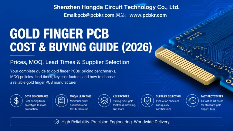
  • Gold finger PCB cost and buying guide featuring hard gold edge connector pricing, MOQ, and manufacturing benchmarks by Hongda Circuit
    Blog

    Gold Finger PCB Cost & Buying Guide: Prices, MOQ, Lead Times & Supplier Selection

    ByDavid 07/28/202608/04/2026

    Gold Finger PCB Cost Quick Summary: Gold finger PCBs remain the gold standard for edge connectors in high-insertion applications. In 2026, selective hard gold plating, precision beveling, and advanced nickel barrier technologies continue to dominate the landscape. This guide breaks down real pricing factors, lead time realities, and what separates a reliable gold finger PCB…

    Read More Gold Finger PCB Cost & Buying Guide: Prices, MOQ, Lead Times & Supplier SelectionContinue

  • 推荐版本: PCB Gold fingers edge connector with selective hard gold plating and precision beveling by Hongda Circuit
    Blog

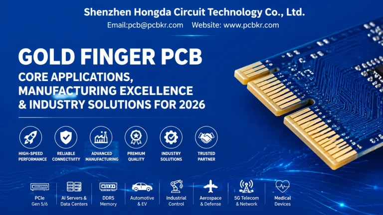
    Gold Finger PCB: Core Applications, Manufacturing Excellence & Industry Solutions

    ByDavid 07/28/202608/04/2026

    PCB Gold fingers edge connector: Why Gold Finger PCB Technology Defines Modern Interconnect Reliability A gold finger PCB—also referred to as an edge connector PCB or electroplated gold PCB—is not merely a surface finish choice. It is a mission-critical interface engineering decision. The gold-plated contact pads running along the board edge serve as the primary…

    Read More Gold Finger PCB: Core Applications, Manufacturing Excellence & Industry SolutionsContinue

  • Gold Finger PCB Specifications & IPC Class 3 Plating Guide by Shenzhen Hongda Circuit
    Blog

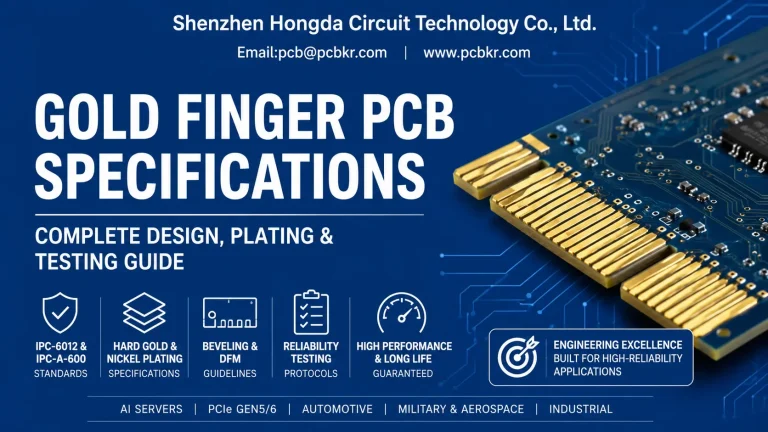
    Gold Finger PCB Specifications & IPC Standards: Complete Design, Plating & Testing Guide

    ByDavid 07/27/202608/04/2026

    Gold Finger PCB Specifications: This guide covers full IPC standards, plating stackup, mechanical design, reliability testing and supplier selection for gold finger edge connector PCBs, including Class 2 / Class 3 performance difference, hard gold vs ENIG comparison, as well as high-reliability application requirements for PCIe, automotive and military scenarios. What Are Gold Finger PCBs…

    Read More Gold Finger PCB Specifications & IPC Standards: Complete Design, Plating & Testing GuideContinue

  • Comprehensive breakdown of gold finger PCB manufacturing process featuring IPC Class 3 standards, cobalt-alloy hard gold plating, and precision beveling capabilities by Hongda Circuit.
    Blog

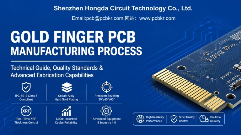
    Gold Finger PCB Manufacturing Process: Technical Guide, Quality Standards & Advanced Fabrication Capabilities

    ByDavid 07/27/202608/04/2026

    Gold finger PCBs remain the backbone of high-reliability interconnection across server backplanes, PCIe expansion cards, industrial control modules, and telecommunications infrastructure. Yet procurement engineers and hardware designers consistently face the same field failures: premature gold wear at the contact edge, nickel barrier corrosion after 500+ insertion cycles, impedance drift caused by uneven plating thickness, and…

    Read More Gold Finger PCB Manufacturing Process: Technical Guide, Quality Standards & Advanced Fabrication CapabilitiesContinue

Page navigation

Previous PagePrevious 1 … 24 25 26 27 28 … 44 Next PageNext

Shenzhen Hongda Circuit Technology Co., Ltd

Address: Room 1608-1610, Research Development Comprehensive Building, Baoyunda Logistics Center, Baoan, Shenzhen, China

E-mail:sales@pcbkr.com

TEL:+86 0755 23720053

Industry Insight Blog

PCB manufacturer

High-Frequency PCB

HDI PCB

Multilayer PCB

Metal Core PCB

High-Speed PCB

Heavy Copper PCB

Flex PCB

Rigid-Flex PCB

IC Substrates PCB

Technology

120-Layer 5G-Advanced/6G Communication Boards

High-Speed Semiconductor Test Boards

mSAP-Processed IC Package Substrates

Specialized Millimeter-Wave Radar PCBs

224Gbps High-Frequency Microwave Circuits

Intelligent Industrial Control PCBs

© 2026 Shenzhen Hongda Circuit Technology Co., Ltd.

  • Home
  • PCB Products
    • High-Frequency PCB
    • HDI PCB
    • Multilayer PCB
    • Metal Core PCB
    • High-Speed PCB
    • Heavy Copper PCB
    • Flex PCB
    • Rigid-Flex PCB
    • IC Substrates PCB
  • PCB Assembly
    •  Advanced BGA & SMT 
    • Box Build & Cable Assy 
    • Component Sourcing
    • Turnkey & Consignment
  • Capability Overview
    • Capability
    • Advanced Equipment
    • PCB Design & Eng.
    • Standard PCB Capability
    • IC Substrate Capability
    • HDI PCB Capability
    • Rigid-Flex Capability
    • RF PCB Capability
    • High frequency PCBs Capability
  • Technology
    • 120-Layer 5G-Advanced/6G Communication Boards
    • High-Speed Semiconductor Test Boards
    • mSAP-Processed IC Package Substrates
    • Specialized Millimeter-Wave Radar PCBs
    • 224Gbps High-Frequency Microwave Circuits
    • Intelligent Industrial Control PCBs
    • FAQ
  • Blog
  • About Us
    • Certifications
  • Contact