Skip to content
PCBkr.com
  • Home
  • PCB ProductsExpand
    • High-Frequency PCB
    • HDI PCB
    • Multilayer PCB
    • Metal Core PCB
    • High-Speed PCB
    • Heavy Copper PCB
    • Flex PCB
    • Rigid-Flex PCB
    • IC Substrates PCB
  • PCB AssemblyExpand
    •  Advanced BGA & SMT 
    • Box Build & Cable Assy 
    • Component Sourcing
    • Turnkey & Consignment
  • Capability OverviewExpand
    • Capability
    • Advanced Equipment
    • PCB Design & Eng.
    • Standard PCB Capability
    • IC Substrate Capability
    • HDI PCB Capability
    • Rigid-Flex Capability
    • RF PCB Capability
    • High frequency PCBs Capability
  • TechnologyExpand
    • 120-Layer 5G-Advanced/6G Communication Boards
    • High-Speed Semiconductor Test Boards
    • mSAP-Processed IC Package Substrates
    • Specialized Millimeter-Wave Radar PCBs
    • 224Gbps High-Frequency Microwave Circuits
    • Intelligent Industrial Control PCBs
    • FAQ
  • Blog
  • About UsExpand
    • Certifications
  • Contact
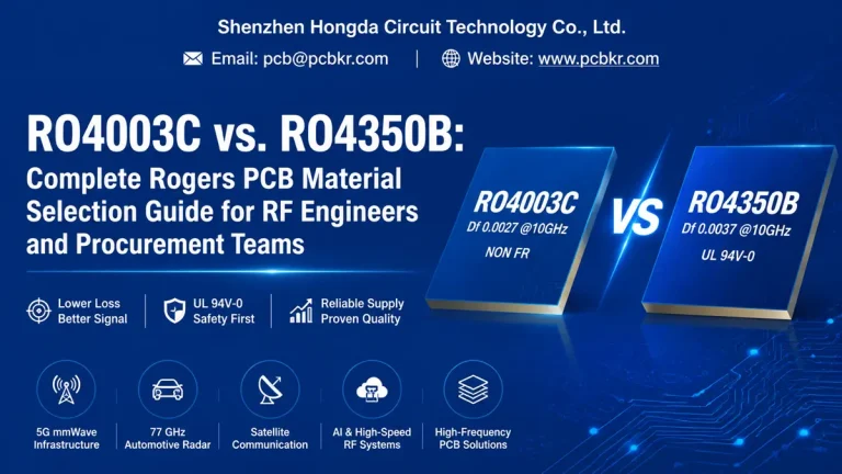
  • RO4003C vs RO4350B Rogers PCB material selection guide comparing loss factor, UL 94V-0 rating, and RF applications by Hongda Circuit
    Blog

    RO4003C vs. RO4350B: Complete Rogers PCB Material Selection Guide for RF Engineers and Procurement Teams

    ByDavid 08/11/202608/11/2026

    Choosing the right Rogers PCB material directly determines whether your high‑frequency design meets its insertion‑loss budget, passes thermal cycling qualification, and ships on time. In 2026, with 5G mmWave infrastructure expanding, 77 GHz automotive radar volumes surging, and AI‑driven RF systems demanding tighter tolerances, the debate between Rogers RO4003C and RO4350B has moved from a…
    Read More RO4003C vs. RO4350B: Complete Rogers PCB Material Selection Guide for RF Engineers and Procurement TeamsContinue

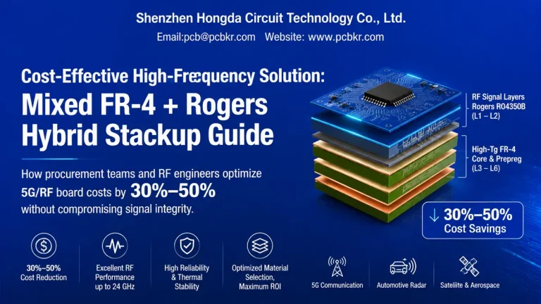
  • Rogers RO4350B + FR4 Mixed Delectrics PCB hybrid stackup architecture by Hongda Circuit
    Blog

    Cost‑Effective High‑Frequency Solution: Mixed FR‑4 + Rogers Hybrid Stackup Guide

    ByDavid 08/10/202608/10/2026

    How procurement teams and RF engineers optimize 5G/RF board costs by 30%–50% without compromising signal integrity. The Cost vs. Physics Dilemma in Multilayer RF PCBs As highlighted in our foundational pillar guide, “The Definitive Guide to Rogers PCB: Material Properties, Manufacturing & RF Applications,” high‑frequency designs above 5 GHz transition from a pure cost decision…

    Read More Cost‑Effective High‑Frequency Solution: Mixed FR‑4 + Rogers Hybrid Stackup GuideContinue

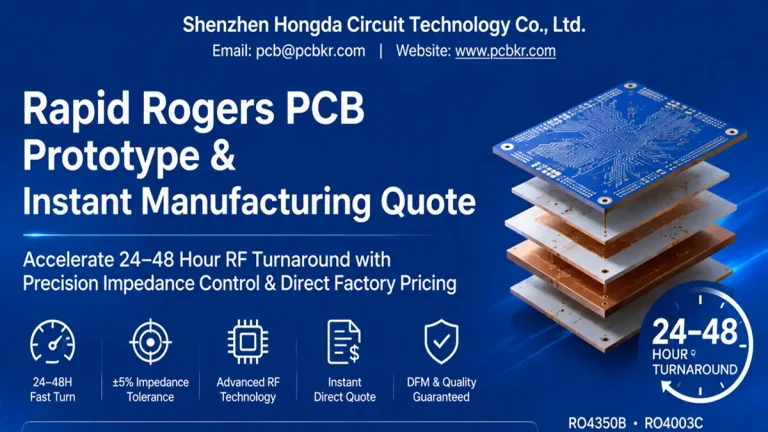
  • rogers 4350 pcb cheap with precision impedance control by Hongda Circuit
    Blog

    Rapid Rogers PCB Prototype & Instant Manufacturing Quote

    ByDavid 08/10/202608/10/2026

    Accelerate 24‑48 Hour RF Turnaround with Precision Impedance Control & Direct Factory Pricing Rogers 4350B PCB cheap high‑frequency hardware development does not mean compromising performance, as transitioning an RF circuit from simulation to physical reality is fraught with speed and precision bottlenecks. Engineering and procurement teams often encounter severe friction: prototype turnaround times extending into…

    Read More Rapid Rogers PCB Prototype & Instant Manufacturing QuoteContinue

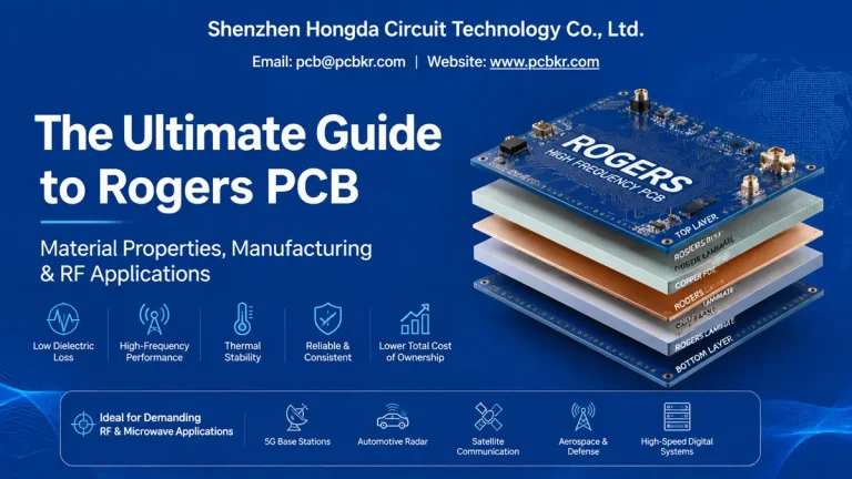
  • Ultimate Guide to Rogers PCB materials, high-frequency properties, and RF applications by Shenzhen Hongda Circuit Technology
    Blog

    The Definitive Guide to Rogers PCB: Material Properties, Manufacturing & RF Applications

    ByDavid 08/10/202608/10/2026

    When a procurement team sources a Rogers PCB for the first time, the gap between a standard FR‑4 quote and a Rogers laminate quotation often triggers sticker shock—sometimes 3× to 5× higher per square meter. Yet seasoned RF engineers know that above 5 GHz, material choice stops being a cost decision and becomes a physics…

    Read More The Definitive Guide to Rogers PCB: Material Properties, Manufacturing & RF ApplicationsContinue

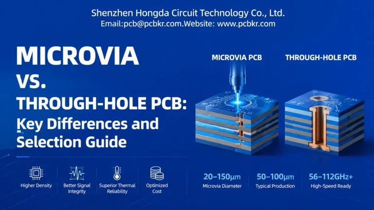
  • Cross-section comparison of microvias PCB and through-hole PCB technologies by Shenzhen Hongda Circuit Technology
    Blog

    Microvia vs. Through-Hole PCB: Key Differences and Selection Guide

    ByDavid 08/06/202608/07/2026

    When procurement teams and hardware engineers search for microvias pcb solutions, they are often at a crossroads: stick with the familiar through-hole technology or migrate to laser-drilled microvias. The choice is not merely a matter of miniaturization—it directly impacts signal integrity, manufacturing cost, thermal reliability, and whether your design can support next-generation AI server or…

    Read More Microvia vs. Through-Hole PCB: Key Differences and Selection GuideContinue

  • supply chain guide from Shenzhen Hongda Circuit Technology Co., Ltd. for global procurement teams sourcing high-reliability microvia PCBs from China. Contains email and website details.
    Blog

    Sourcing High-Reliability Microvia PCBs from China: Supply Chain Guide for Global Procurement Teams

    ByDavid 08/06/202608/07/2026

    China microvias pcb manufacturer vetting is top‑of‑mind for procurement engineers and supply chain managers assessing China‑based HDI PCB partners. The question is no longer “Can they build it?”—it’s “Can they build it consistently, ship it compliantly, and support it globally?” The New Geography of Microvia Manufacturing In 2026, approximately 68% of advanced HDI and microvia…

    Read More Sourcing High-Reliability Microvia PCBs from China: Supply Chain Guide for Global Procurement TeamsContinue

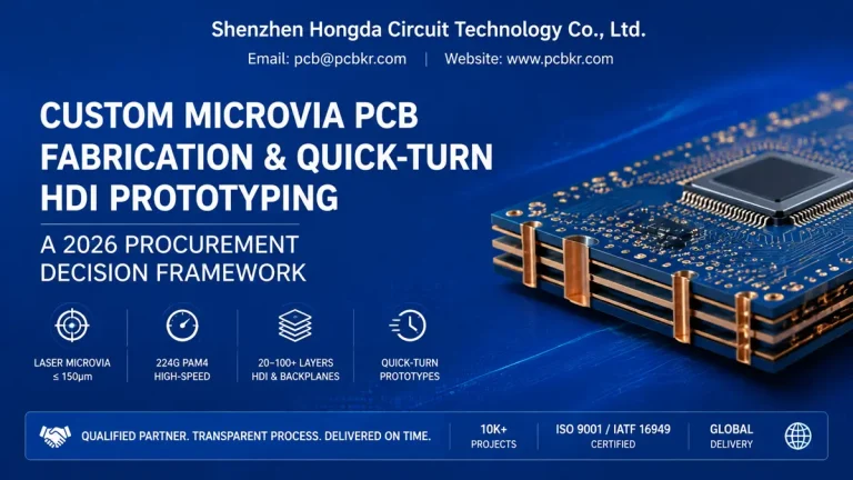
  • Custom Microvia PCB Fabrication and Quick-Turn HDI Prototyping: A 2026 Procurement Decision Framework Banner by Shenzhen Hongda Circuit Technology
    Blog

    Custom Microvia PCB Fabrication & Quick-Turn HDI Prototyping: A 2026 Procurement Decision Framework

    ByDavid 08/06/202608/07/2026

    If you are a procurement engineer, supply chain manager, or hardware program director sourcing custom HDI PCB manufacturers in 2026, our full overseas buying manual is Sourcing High-Reliability Microvia PCBs from China: Supply Chain Guide for Global Procurement Teams. This is not a temporary shortage. The convergence of AI server clusters, 1.6T optical modules, and…

    Read More Custom Microvia PCB Fabrication & Quick-Turn HDI Prototyping: A 2026 Procurement Decision FrameworkContinue

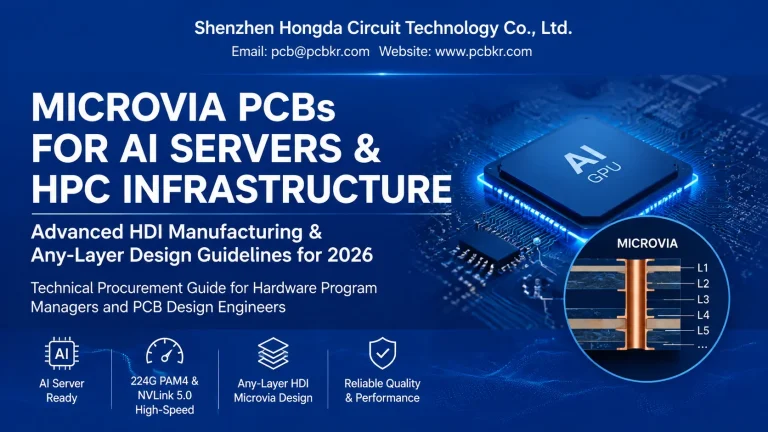
  • Microvia PCBs for AI servers and HPC infrastructure featuring any-layer HDI manufacturing and 224G PAM4 technology by Hongda Circuit
    Blog

    Microvia PCBs for AI Servers and HPC Infrastructure: Advanced HDI Manufacturing & Any-Layer Design Guidelines

    ByDavid 08/06/202608/07/2026

    From Generic HDI to Application-Specific Microvia Architecture The preceding pillar guide, High-Density Interconnect (HDI) Microvia PCB Manufacturing | mSAP & SAP Capabilities for AI Server and HPC Applications, established the manufacturing fundamentals of HDI microvia technology—laser drilling thresholds, mSAP versus SAP process economics, and the certification landscape that separates qualified suppliers from marketing brochures. This…

    Read More Microvia PCBs for AI Servers and HPC Infrastructure: Advanced HDI Manufacturing & Any-Layer Design GuidelinesContinue

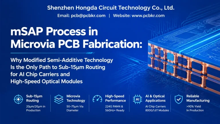
  • mSAP process PCB fabrication showing sub-15um routing, microvias, and high-speed design capabilities by Hongda Circuit
    Blog

    mSAP Process in Microvia PCB Fabrication: Why Modified Semi-Additive Technology Is the Only Path to Sub-15μm Routing for AI Chip Carriers and High-Speed Optical Modules

    ByDavid 08/05/202608/07/2026

    Introduction: The Subtractive Etching Ceiling and Why mSAP Became Unavoidable in 2026 If you are a hardware procurement manager sourcing microvia PCBs for AI infrastructure in 2026, you have likely encountered a frustrating reality: your design team specifies 20 μm line/space for a GPU carrier board or 25 μm for an 800G optical module, and…

    Read More mSAP Process in Microvia PCB Fabrication: Why Modified Semi-Additive Technology Is the Only Path to Sub-15μm Routing for AI Chip Carriers and High-Speed Optical ModulesContinue

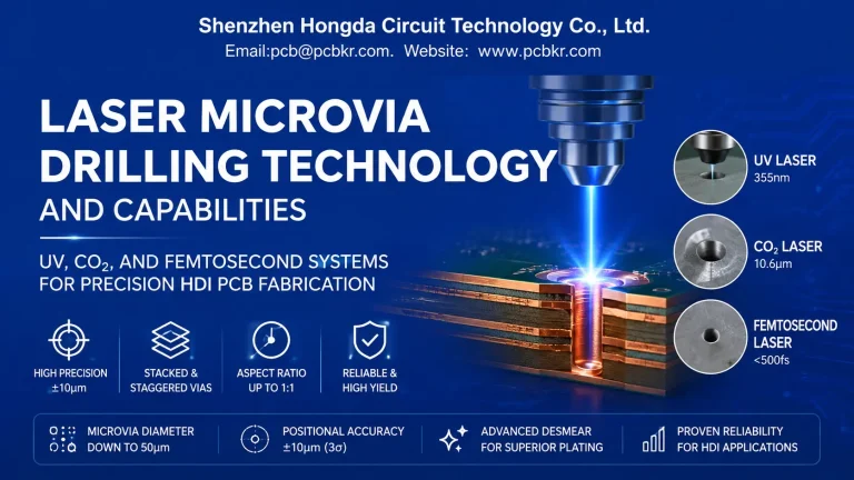
  • HDI laser microvia PCB capabilities and laser drilling technology overview showing UV, CO2, and femtosecond laser systems by Hongda Circuit
    Blog

    Laser Microvia Drilling Technology and Capabilities: UV, CO₂, and Femtosecond Systems for Precision HDI PCB Fabrication

    ByDavid 08/05/202608/07/2026

    Introduction: The Laser as the Defining Tool of Modern HDI Manufacturing In the hierarchy of PCB manufacturing capabilities, laser microvia drilling sits at the intersection of physics, precision engineering, and production economics. No other single process step has as much impact on the density, reliability, and electrical performance of a high-density interconnect (HDI) board. And…

    Read More Laser Microvia Drilling Technology and Capabilities: UV, CO₂, and Femtosecond Systems for Precision HDI PCB FabricationContinue

Page navigation

Previous PagePrevious 1 … 22 23 24 25 26 … 44 Next PageNext

Shenzhen Hongda Circuit Technology Co., Ltd

Address: Room 1608-1610, Research Development Comprehensive Building, Baoyunda Logistics Center, Baoan, Shenzhen, China

E-mail:sales@pcbkr.com

TEL:+86 0755 23720053

Industry Insight Blog

PCB manufacturer

High-Frequency PCB

HDI PCB

Multilayer PCB

Metal Core PCB

High-Speed PCB

Heavy Copper PCB

Flex PCB

Rigid-Flex PCB

IC Substrates PCB

Technology

120-Layer 5G-Advanced/6G Communication Boards

High-Speed Semiconductor Test Boards

mSAP-Processed IC Package Substrates

Specialized Millimeter-Wave Radar PCBs

224Gbps High-Frequency Microwave Circuits

Intelligent Industrial Control PCBs

© 2026 Shenzhen Hongda Circuit Technology Co., Ltd.

  • Home
  • PCB Products
    • High-Frequency PCB
    • HDI PCB
    • Multilayer PCB
    • Metal Core PCB
    • High-Speed PCB
    • Heavy Copper PCB
    • Flex PCB
    • Rigid-Flex PCB
    • IC Substrates PCB
  • PCB Assembly
    •  Advanced BGA & SMT 
    • Box Build & Cable Assy 
    • Component Sourcing
    • Turnkey & Consignment
  • Capability Overview
    • Capability
    • Advanced Equipment
    • PCB Design & Eng.
    • Standard PCB Capability
    • IC Substrate Capability
    • HDI PCB Capability
    • Rigid-Flex Capability
    • RF PCB Capability
    • High frequency PCBs Capability
  • Technology
    • 120-Layer 5G-Advanced/6G Communication Boards
    • High-Speed Semiconductor Test Boards
    • mSAP-Processed IC Package Substrates
    • Specialized Millimeter-Wave Radar PCBs
    • 224Gbps High-Frequency Microwave Circuits
    • Intelligent Industrial Control PCBs
    • FAQ
  • Blog
  • About Us
    • Certifications
  • Contact