Skip to content
PCBkr.com
  • Home
  • PCB ProductsExpand
    • High-Frequency PCB
    • HDI PCB
    • Multilayer PCB
    • Metal Core PCB
    • High-Speed PCB
    • Heavy Copper PCB
    • Flex PCB
    • Rigid-Flex PCB
    • IC Substrates PCB
  • PCB AssemblyExpand
    •  Advanced BGA & SMT 
    • Box Build & Cable Assy 
    • Component Sourcing
    • Turnkey & Consignment
  • Capability OverviewExpand
    • Capability
    • Advanced Equipment
    • PCB Design & Eng.
    • Standard PCB Capability
    • IC Substrate Capability
    • HDI PCB Capability
    • Rigid-Flex Capability
    • RF PCB Capability
    • High frequency PCBs Capability
  • TechnologyExpand
    • 120-Layer 5G-Advanced/6G Communication Boards
    • High-Speed Semiconductor Test Boards
    • mSAP-Processed IC Package Substrates
    • Specialized Millimeter-Wave Radar PCBs
    • 224Gbps High-Frequency Microwave Circuits
    • Intelligent Industrial Control PCBs
    • FAQ
  • Blog
  • About UsExpand
    • Certifications
  • Contact
  • Gold Finger PCB Design Guide: Complete Technical Reference for Dimensions, Chamfer, Plating & DFM
    Blog

    Gold Finger PCB Design Guide: Complete Technical Reference for Dimensions, Chamfer, Plating & DFM

    ByDavid 07/27/202608/04/2026

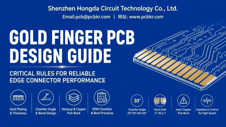
    By Shenzhen Hongda Circuit Technology Co., Ltd. | Engineering TeamLast Updated: July 2026 | Technical Depth: Advanced | Target Audience: PCB Designers, Hardware Engineers, Procurement Technical Reviewers Introduction: Why Gold Finger Design Decisions Determine Product Reliability A gold finger PCB design that looks correct on a schematic can fail catastrophically in the field if chamfer…
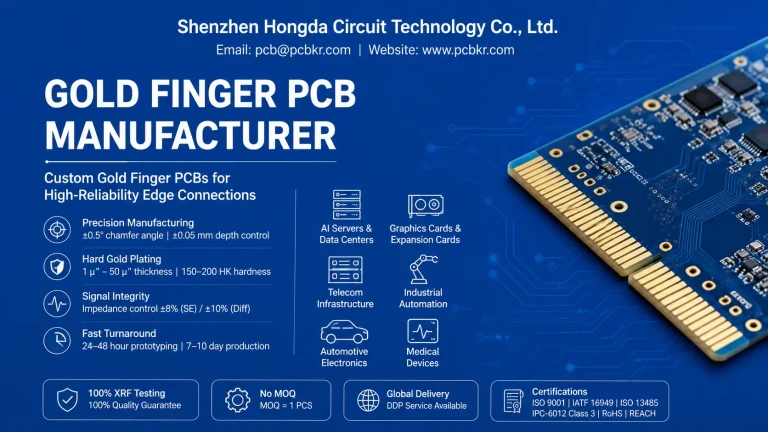
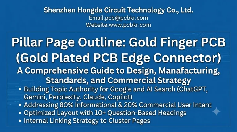
    Read More Gold Finger PCB Design Guide: Complete Technical Reference for Dimensions, Chamfer, Plating & DFMContinue

  • Shenzhen Hongda Circuit Gold Finger PCB Manufacturer and Factory Capabilities
    Blog

    Leading China Gold Finger PCB Manufacturer & Custom Factory

    ByDavid 07/27/202608/04/2026

    High-Precision Hard/Soft Gold Finger PCBs from Rapid Prototyping to High-Volume ProductionISO 9001 | IATF 16949 | UL Certified | IPC-6012 Class 3 | 15+ Years Gold Finger Expertise Why Partner with Us as Your Gold Finger PCB Supplier? When sourcing gold finger PCBs, procurement teams and design engineers face four critical pain points that separate…

    Read More Leading China Gold Finger PCB Manufacturer & Custom FactoryContinue

  • Gold Finger PCB
    Blog

    Gold Finger PCB: Design, Manufacturing, Standards & Cost Guide

    ByDavid 07/24/202608/04/2026

    What Is a Gold Finger PCB and Why Does It Matter? A Gold Finger PCB (also called Gold Finger Printed Circuit Board, Gold Plated PCB Edge, or PCB Edge Connector) is a specialized circuit board featuring electroplated hard gold contacts along one or more edges. These gold-plated edge connectors—commonly referred to as gold fingers, PCB…

    Read More Gold Finger PCB: Design, Manufacturing, Standards & Cost GuideContinue

  • Blind Via PCB Reliability Testing Guide by Shenzhen Hongda Circuit Technology
    Blog

    Blind Via PCB Reliability Testing: Complete Guide to Qualification, IPC Standards & Failure Analysis

    ByDavid 07/24/202608/05/2026

    Introduction: Why Blind Via Reliability Defines HDI PCB Performance In the era of AI-driven computing, autonomous vehicles, and 5G telecommunications, blind via PCB reliability testing has emerged as the single most critical qualification criterion for high-density interconnect (HDI) boards. Unlike through-hole vias that traverse the entire board thickness, blind vias connect outer layers to one…

    Read More Blind Via PCB Reliability Testing: Complete Guide to Qualification, IPC Standards & Failure AnalysisContinue

  • Blind via PCB cost breakdown and optimization guide 2026 by Hongda Circuit
    Blog

    Blind Via PCB Cost Guide: Price Breakdown, Cost Drivers & Money-Saving Tips

    ByDavid 07/24/202608/05/2026

    Introduction: Why Blind Via PCB Pricing Demands Strategic Understanding Blind via technology sits at the intersection of performance necessity and cost sensitivity. Every procurement manager who has requested an HDI PCB quote has faced the same question: why does adding a few laser-drilled vias multiply the board cost by two, three, or even five times?…

    Read More Blind Via PCB Cost Guide: Price Breakdown, Cost Drivers & Money-Saving TipsContinue

  • Technical guide for Blind Via PCB Reliability Testing, covering qualification, IPC standards, and failure analysis. Published by Shenzhen Hongda Circuit Technology Co., Ltd.
    Blog

    Blind Via PCB Reliability Testing: Complete Guide to Qualification, IPC Standards & Failure Analysis

    ByDavid 07/24/202607/24/2026

    Introduction: Why Blind Via Reliability Defines the Future of HDI PCB Manufacturing Blind vias are the Achilles’ heel of High-Density Interconnect (HDI) printed circuit boards. While they enable the extraordinary routing density that modern electronics demand, they also concentrate mechanical stress, thermal gradients, and electrical current in the smallest possible footprint. In the era of…

    Read More Blind Via PCB Reliability Testing: Complete Guide to Qualification, IPC Standards & Failure AnalysisContinue

  • Blind Via PCB Materials
    Blog

    Blind Via PCB Materials: Complete Selection Guide for HDI, High-Speed & High-Reliability Applications

    ByDavid 07/23/202608/05/2026

    Table of Contents What Materials Are Used in Blind Via PCB? Blind via PCB technology sits at the intersection of structural engineering and materials science. Unlike through-hole vias that penetrate the entire board, blind vias connect only specific layer pairs—typically from an outer surface to one or more internal layers. This structural distinction makes material…

    Read More Blind Via PCB Materials: Complete Selection Guide for HDI, High-Speed & High-Reliability ApplicationsContinue

  • Blind Via vs Buried Via PCB
    Blog

    Blind Via vs Buried Via PCB: Which One Is Better for HDI PCB Design

    ByDavid 07/23/202608/05/2026

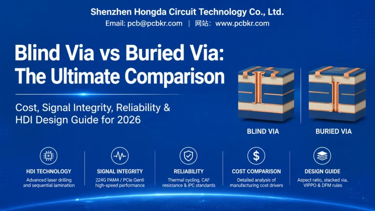
    A blind via connects an outer layer to one or more inner layers and remains visible on the finished PCB surface. A buried via connects only internal layers and is completely hidden after lamination. Neither is universally “better”—the right choice depends on routing density, signal speed, layer count, and cost constraints. For 2026 AI server…

    Read More Blind Via vs Buried Via PCB: Which One Is Better for HDI PCB DesignContinue

  • Buried Via PCB Supplier | Custom HDI | Free DFM — Hongda
    Blog

    Buried Via HDI PCB Design & Fabrication Handbook: Sequential Lamination, Reliability & Cost Optimization for 224G High-Speed Hardware

    ByDavid 07/23/202608/05/2026

    For multilayer HDI PCBs targeting 224G PAM4, PCIe Gen6 and 800G Ethernet hardware, buried vias deliver unmatched signal integrity by creating fully internal interlayer copper connections with zero transmission line stubs. Unlike blind microvias that link outer surfaces to inner layers, buried vias are encapsulated entirely within core inner sub-assemblies, reserving 100% of top and…

    Read More Buried Via HDI PCB Design & Fabrication Handbook: Sequential Lamination, Reliability & Cost Optimization for 224G High-Speed HardwareContinue

  • Blind Via PCB ultimate guide banner showing cross-section microvia structure by Hongda Circuit
    Blog

    What Is a Blind Via PCB? Complete Design, Manufacturing & Cost Guide

    ByDavid 07/23/202608/05/2026

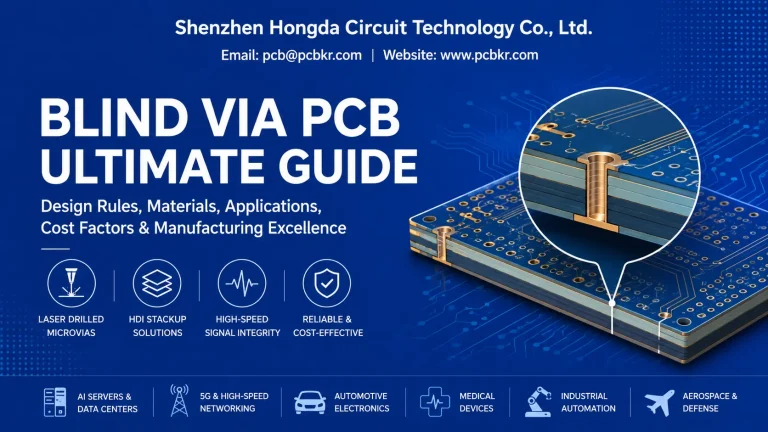
    A blind via PCB uses plated holes that connect an outer layer to one or more inner layers without passing through the entire circuit board. For complete fabrication specifications, stackups, and cost drivers across all interconnect types, see our master guide on blind & buried via PCB manufacturing. What Is a Blind Via PCB? Blind…

    Read More What Is a Blind Via PCB? Complete Design, Manufacturing & Cost GuideContinue

Page navigation

Previous PagePrevious 1 … 25 26 27 28 29 … 44 Next PageNext

Shenzhen Hongda Circuit Technology Co., Ltd

Address: Room 1608-1610, Research Development Comprehensive Building, Baoyunda Logistics Center, Baoan, Shenzhen, China

E-mail:sales@pcbkr.com

TEL:+86 0755 23720053

Industry Insight Blog

PCB manufacturer

High-Frequency PCB

HDI PCB

Multilayer PCB

Metal Core PCB

High-Speed PCB

Heavy Copper PCB

Flex PCB

Rigid-Flex PCB

IC Substrates PCB

Technology

120-Layer 5G-Advanced/6G Communication Boards

High-Speed Semiconductor Test Boards

mSAP-Processed IC Package Substrates

Specialized Millimeter-Wave Radar PCBs

224Gbps High-Frequency Microwave Circuits

Intelligent Industrial Control PCBs

© 2026 Shenzhen Hongda Circuit Technology Co., Ltd.

  • Home
  • PCB Products
    • High-Frequency PCB
    • HDI PCB
    • Multilayer PCB
    • Metal Core PCB
    • High-Speed PCB
    • Heavy Copper PCB
    • Flex PCB
    • Rigid-Flex PCB
    • IC Substrates PCB
  • PCB Assembly
    •  Advanced BGA & SMT 
    • Box Build & Cable Assy 
    • Component Sourcing
    • Turnkey & Consignment
  • Capability Overview
    • Capability
    • Advanced Equipment
    • PCB Design & Eng.
    • Standard PCB Capability
    • IC Substrate Capability
    • HDI PCB Capability
    • Rigid-Flex Capability
    • RF PCB Capability
    • High frequency PCBs Capability
  • Technology
    • 120-Layer 5G-Advanced/6G Communication Boards
    • High-Speed Semiconductor Test Boards
    • mSAP-Processed IC Package Substrates
    • Specialized Millimeter-Wave Radar PCBs
    • 224Gbps High-Frequency Microwave Circuits
    • Intelligent Industrial Control PCBs
    • FAQ
  • Blog
  • About Us
    • Certifications
  • Contact