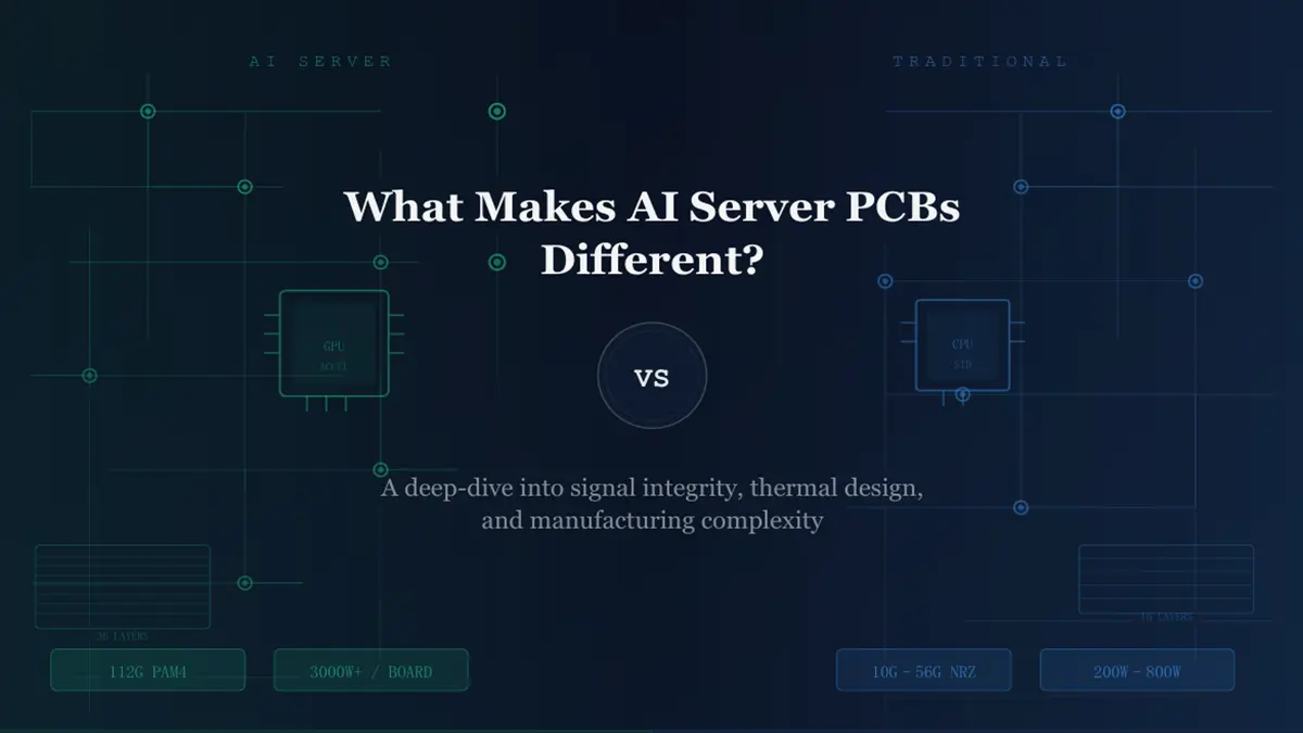
What Makes AI Server PCBs Different From Traditional Enterprise PCBs?
The global shift toward high-performance computing and artificial intelligence infrastructure has sparked a major technological evolution in data center hardware. When analyzing the core infrastructure supporting this revolution, evaluating the engineering requirements of an AI Server PCB vs. Traditional PCB architecture reveals a massive technical chasm. As generative AI models grow exponentially, traditional enterprise server motherboards can no longer handle the massive computing loads, ultra-high data rates, and extreme thermal profiles required by next-generation accelerators. For hardware procurement professionals and system architects evaluating vendor capabilities for high-speed hardware, understanding these differences is critical for optimizing system reliability and cost-to-performance ratios.
The Core Technical Baseline: Architecture & Electrical Demands
The fundamental divergence between these two board types lies in their baseline layout complexity and signal transmission capacity. While traditional enterprise hardware targets baseline operational stability and cost efficiency, AI hardware is engineered strictly around signal integrity at microwave frequencies.
| Comparison Area | AI Server PCB | Traditional Enterprise PCB |
|---|---|---|
| Primary Application | AI training servers, GPU clusters, AI accelerators | Database servers, storage servers |
| Typical Layer Count | 20–36 layers | 8–16 layers |
| Data Rate Support | 112G PAM4 / 224G PAM4 | 10G–56G NRZ/PAM4 |
| Signal Frequency | 30–60 GHz+ | <15 GHz |
| PCB Dimension | Large-scale footprint | Standard server size |
| Routing Density | Extremely high | Moderate |
| Power Consumption | 1000W–3000W+ per board | 200W–800W |
1. Advanced Substrate Materials and Dielectric Behavior
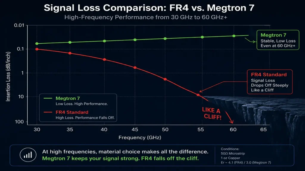
Insertion Loss Comparison ($dB/inch$) between FR4 and Megtron 7 from 30 GHz to 60 GHz+
When routing signals for 112G and 224G PAM4 architectures, material insertion loss becomes the primary bottleneck for system engineers. This requires a complete migration away from standard legacy laminates toward ultra-low-loss substrate materials.
AI Server Substrate Dynamics
To successfully transmit data rates up to 224G PAM4 without catastrophic attenuation, AI hardware utilizes highly specialized, high-frequency laminates:
- Commonly Specified Materials: Panasonic Megtron 6, Panasonic Megtron 7, Isola I-Speed, Isola Tachyon 100G, Rogers hybrid stackups, and Shengyi S1000-2M.
- Key Properties: These materials deliver an ultra-low Dielectric Dissipation Factor (Df) of 0.002 to 0.004, highly stable Dielectric Constants (Dk), and exceptional high-frequency performance capable of supporting bandwidths beyond 56 GHz.
Traditional Enterprise Substrate Dynamics
Conversely, standard enterprise networking platforms operate on significantly lower network speeds, minimizing the need for premium dielectric materials:
- Commonly Specified Materials: Standard FR4, Shengyi S1000H, IT-180A, and TU-872.
- Key Properties: These laminates exhibit a much higher Df (0.012–0.020) and are restricted to frequencies below 15 GHz, though they offer highly mature, cost-effective processing for 10G to 40G applications.
| Laminate Property | AI Server PCB Materials | Enterprise-Grade PCB Materials |
|---|---|---|
| Dielectric Dissipation Factor (Df) | 0.002–0.004 | 0.012–0.020 |
| Glass Transition Temp (Tg) | >180°C | 150–170°C |
| Frequency Capabilities | 56 GHz+ | <15 GHz |
| Relative Material Cost Ratio | Extremely High | Low Base |
2. Ultra-High-Density Manufacturing and Via Technologies
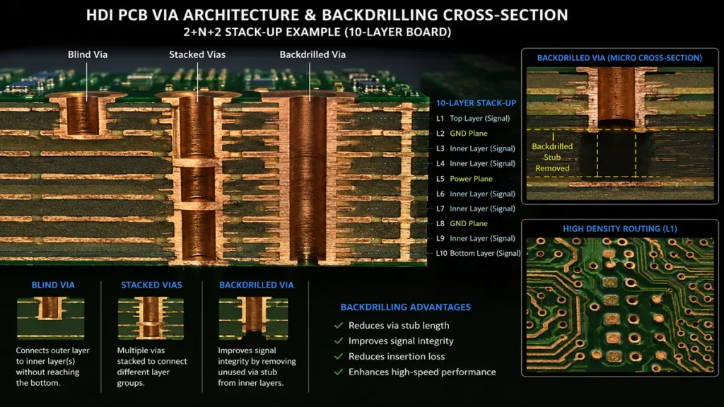
Micro-Section Architecture of Advanced HDI PCB Demonstrating Laser Blind Vias, Stacked Vias, and Precision Depth Controlled Backdrilling to Eliminate Via Stubs.
The tight pin-pitch of modern high-performance GPU clusters demands advanced High-Density Interconnect (HDI) manufacturing methodologies that are rarely required in baseline server production.
High-Precision Fabrication Rules
- Laser Direct Imaging (LDI): AI server boards mandate LDI fabrication to secure a strict ±10 μm trace precision. This enables ultra-fine trace width and spacing design rules down to 2/2 mil or 2.5/2.5 mil spacing configurations.
- Sequential Lamination: To accommodate complex internal routing without trace degradation, boards feature complex build-ups such as 2+N+2, 3+N+3, or any-layer HDI structures to compress signal paths.
- Automated X-Ray Registration: Given the risks of layer shifting in a 36-layer stackup, automated X-ray alignment and internal layer compensation are implemented to lock in an interlayer registration accuracy of less than 50 μm.
Via Engineering and Stub Elimination
| Via Interconnect Feature | AI Server PCB Design | Enterprise PCB Design |
|---|---|---|
| Primary Interconnect Type | Laser Microvias | Standard Mechanical Through-Hole |
| Typical Via Diameter | 75–100 μm | 200–300 μm |
| Interconnect Via Density | Extremely High | Moderate |
| Via Stub Removal Requirements | Mandatory Backdrilling | Generally Unnecessary |
| HDI Architectural Integration | Strict Requirement | Rarely Applied |
3. Strict Signal Integrity (SI) and Impedance Control
What are the signal integrity requirements for 112G and 224G channels?
AI platforms operating on 112G/224G PAM4 signaling protocols, PCIe Gen6/Gen7 bus standards, and 800G to 1.6T Ethernet switches require tight control over channel parasitics. Engineers focus heavily on mitigating insertion loss, return loss, crosstalk, and deterministic jitter. To preserve signal fidelity across long trace runs, standard impedance tolerances are tightened from the conventional ±10% down to a highly demanding ±5% or ±3% tolerance window. Standard corporate systems running PCIe Gen3 or Gen4 and 10G/25G Ethernet handle much looser signal constraints, allowing standard fabrication houses to manufacture them without specialized high-speed test fixtures.
4. Heavy Copper and Advanced Thermal Management
3D Partial Cross-Section of an AI Accelerator Board Featuring 2oz–4oz Heavy Copper Inners for High Current Capacity and an Embedded Solid Copper Coin for Localized GPU/MOSFET Thermal Management.
The immense processing power of modern hardware generates significant thermal loads, introducing severe thermal management challenges that impact the entire PCB layout.
- Heavy Copper Infrastructure: AI accelerator systems frequently draw massive current, necessitating internal power layers built with 2 oz, 3 oz, or even 4 oz heavy copper to prevent localized IR drop and excessive heating.
- Embedded Copper Coins: For high-density heat dissipation directly beneath high-TDP components like GPUs and ASICs, solid copper coins are embedded directly into the board structure. This provides an uninterrupted, highly conductive thermal path directly to vapor chambers or liquid-cooling cold plates.
- Standard Scaling: Conventional enterprise servers draw far less power (typically 200W–800W) and dissipate heat effectively using standard 1 oz copper planes matched with conventional aluminum heatsinks and forced-air fan arrays.
5. Comprehensive Reliability and High-Speed Signal Testing
Because an unpredicted hardware failure within a massive GPU cluster can stall multi-million dollar LLM training runs, the reliability validation protocols for these boards are intensely thorough.
Advanced Stress Testing
- IST (Interconnect Stress Testing): AI boards undergo mandatory IST protocols to evaluate the mechanical endurance of laser microvias and multi-layer HDI joins under cyclic thermal loads.
- CAF (Conductive Anodic Filament) Resistance: To prevent internal shorts within tightly spaced high-voltage trace paths, high-humidity CAF validation is enforced.
- Extreme Thermal Shock: Boards are subjected to rigorous thermal shock testing, frequently requiring over 1,000 continuous cycles fluctuating between -40°C and +125°C.
High-Speed Channel Validation
Every high-frequency channel undergoes rigorous verification using Vector Network Analyzers (VNA) and Time-Domain Reflectometry (TDR) to map structural impedance profiles. Comprehensive eye diagram analysis ensures that signal margins meet strict receiver specifications before system assembly. In contrast, standard enterprise server validation relies primarily on flying probe tests, Automated Optical Inspection (AOI), and basic functional checks.
6. Sourcing Realities: Total Cost Drivers and Yield Dynamics
Sourcing high-layer-count HDI boards requires an understanding of the underlying manufacturing economics, as cost structures differ significantly from standard product lines.
| Cost Driver Element | AI Server PCB Status | Enterprise PCB Status |
|---|---|---|
| Substrate Raw Cost | Extremely High (Ultra-low loss resins) | Low (Standard FR4 base) |
| Processing Complexity | Mandatory HDI, LDI, and Backdrilling | Standard mechanical drill/print |
| Production Yield Rate | Reduced due to tight stackup tolerances | High baseline manufacturing yields |
| Total Production Cost | 2x to 8x higher than standard baselines | Establishment baseline pricing |
Procurement Engineering Insight
Core Technical Conclusion:
The fundamental difference when comparing an AI Server PCB vs. Traditional PCB is not simply a matter of board real estate or physical dimensions. It is driven by strict demands for ultra-high-speed signal integrity, extreme power distribution density, and high-capacity thermal dissipation. To support 112G/224G PAM4 signalling networks, PCIe Gen6/Gen7 buses, and dense 800G/1.6T switching fabrics, AI hardware requires 20–36 layers, ultra-low-loss laminates (e.g., Megtron 7), complex sequential lamination, microvia HDI configurations, mandatory backdrilling, and strict ±3% impedance limits. Standard corporate server hardware remains focused on cost control and traditional processing, utilizing FR4 materials, 8–16 layer limits, and mechanical through-holes.
How do I select a reliable manufacturing partner for advanced AI PCBs?
When sourcing high-frequency boards, procurement teams must verify that their manufacturing partner has verified expertise in handling complex materials like Megtron 7 or Tachyon 100G. Ensure the facility has advanced fabrication capabilities, such as advanced Laser Direct Imaging (LDI) for fine-line geometry, automated X-ray internal registration control, and high-precision deep backdrilling. Additionally, confirm they have robust validation workflows, including dedicated Interconnect Stress Testing (IST) and Time-Domain Reflectometry (TDR) setups. This ensures the high-yield delivery of advanced boards engineered to support next-generation compute environments.
AI Server vs. Traditional Enterprise PCB Sourcing FAQ
Why must AI server PCBs abandon traditional FR4 materials in favor of premium laminates like Megtron 7 or Tachyon 100G?
The primary driver is the strict requirement for low material dielectric loss (Df) at high frequencies. Traditional enterprise hardware typically operates under 15 GHz, where standard FR4 materials (Df of 0.012–0.020) work effectively at a lower price point. However, AI hardware shifts signal transmission into 112G and 224G PAM4 domains, pushing operating frequencies to 30–60 GHz+. At these speeds, FR4 exhibits extreme insertion loss, leading to severe signal degradation. To guarantee clean signal paths across PCIe Gen6/Gen7 links and 800G/1.6T networks, engineers specify low-loss materials like Megtron 6/7 or Tachyon 100G. These specialty resins provide a stable Dk and an ultra-low Df (0.002–0.004), effectively mitigating high-frequency trace attenuation.
What role does controlled backdrilling play in maintaining signal integrity across 112G/224G PAM4 AI channels?
Controlled-depth backdrilling is mandatory in advanced AI hardware to eliminate via stubs. In standard corporate servers, traces use standard through-holes where unused portions of the via cylinder are left intact. At lower speeds, these stubs do not degrade signals. However, at AI channel frequencies of 30–60 GHz+, these remaining stub sections act as resonant stubs, causing severe signal reflections and crosstalk. Utilizing automated backdrilling to remove the unused copper barrel minimizes impedance disruptions, reduces return loss, and preserves signal integrity across high-speed links.
Why are impedance control tolerances compressed to ±3%–±5% in AI boards compared to standard server baselines?
This tight tolerance window is necessary to protect narrow PAM4 signal eye diagrams from distortion. Traditional server architectures operating on PCIe Gen3 or Gen4 possess higher signal margins, allowing them to function reliably with standard ±10% impedance tolerances. Conversely, 112G and 224G PAM4 networks use multi-level signaling where the structural height of the voltage eyes is highly compressed. Any trace variation or local dielectric shift causes impedance non-uniformity, causing reflections that close the signal eye. Sourcing houses must utilize Laser Direct Imaging (LDI) to hold trace dimensions within ±10 μm and enforce strict ±3% to ±5% impedance limits to maintain channel performance.
How do AI server boards manage the extreme thermal loads produced by dense accelerator clusters like the NVIDIA HGX platform?
AI motherboards integrate heavy copper layers and solid metal inserts to handle the intense thermal outputs of modern GPUs. While standard enterprise servers dissipate 200W–800W using standard 1 oz copper planes and air fans, AI server boards must manage 1000W to 3000W+ per board. To support this, boards incorporate:
Heavy Internal Copper: Employing 2 oz, 3 oz, or 4 oz planes to distribute massive current drops and minimize localized resistive heating.
Embedded Copper Coins: Press-fitting solid copper blocks directly into the substrate beneath high-power GPUs and ASICs to conduct heat away to vapor chambers or liquid-cooling blocks.
Thermal Via Arrays: Placing dense matrices of stitched vias to transfer thermal loads vertically away from active IC footprints.
What commercial and engineering factors explain why AI server PCBs carry a 2x to 8x price premium over traditional options?
The elevated price reflects premium material costs, complex processing steps, and tight manufacturing tolerances. First, the high-frequency base resins (e.g., Megtron 7) cost significantly more than standard FR4. Second, structural layers increase from 8–16 layers to 20–36 layers, requiring multi-stage sequential lamination and complex HDI build-ups (e.g., 2+N+2, 3+N+3). Third, specialized processing—such as 75 μm laser via ablation, precise depth backdrilling, and tight <50 μm layer registration—increases production time. Finally, the strict tolerances required for these boards can lower initial yields compared to mature, standard configurations, resulting in a 2x to 8x cost premium for the finished boards.
Conclusion: Bringing AI-Grade Discipline to Standard PCBs
Navigating the line between cutting-edge innovation and cost-effective mass production shouldn’t be a compromise. At [PCBKR / Hongda Circuit Technology], we bridge this gap by reshaping how everyday hardware is built.
Using top-tier AI server PCB equipment to manufacture traditional PCBs delivers a strategic advantage: interlayer alignment tolerance shrinks from ±75μm to within ±25μm, and differential impedance control tightens to ±5%. Paired with 100% 3D X-Ray inspection, it grants conventional boards chip-level precision, superb signal stability, and near-100% yield.
Our Strategic Partnership to You:
We proudly stand as a strategic partner who possesses the top-tier technical ceiling of the industry’s mega-factories, yet retains the exceptional flexibility and unmatched cost-efficiency required for mid-sized, standard board campaigns. You get zero-defect reliability without paying a premium for tier-1 bureaucracy.
Ready to upgrade your hardware’s reliability?
Submit your Gerber files today for an agile engineering review and a highly competitive quote.
📧 Contact our experts: sales@pcbkr.com
About Author
David Chen https://www.linkedin.com/in/pcbcoming/
David Chen boasts an extensive professional background in PCBA manufacturing, PCBA testing, and PCBA optimization, with specialized expertise in high-precision PCBA fault analysis and rigorous PCBA reliability testing. The author has worked with high-layer-count server PCB fabrication, ultra-low-loss backplane stackups, and thermo-mechanical reliability optimization for AI infrastructure projects involving 112G and 224G PAM4 architectures. Skilled in complex circuit design and cutting-edge advanced PCB manufacturing processes, he delivers solutions that elevate product durability and performance across industrial applications. His technical articles focusing on PCBA manufacturing workflows and testing methodologies are widely cited by industry peers, research institutions, and technical platforms, solidifying his reputation as a recognized technical authority in the global circuit board manufacturing sector.