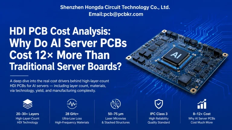
224G PCB Manufacturing: The Complete Engineer’s Guide
Overview
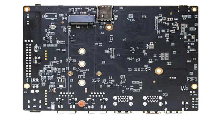
224G PCB manufacturing demands ultra-low-loss laminates with Df ≤ 0.002 at 56 GHz, backdrilling via stubs limited to 8 mil or less, trace width tolerance of ±0.5 mil, and differential impedance controlled within ±5 Ω. At Shenzhen Hongda Circuit Technology Co., Ltd., we produce fully production-qualified 224G circuit boards, complete with full signal integrity simulation support. All finished boards are validated via VNA testing to fully comply with IEEE 802.3ck channel specifications.
What Is 224G PCB Technology and Why Does It Require Unique Manufacturing Standards?
224G refers to PAM4 serial links running at a 112 Gbaud lane rate, delivering a throughput of 224 Gb/s per individual lane. At the Nyquist frequency of 56 GHz, standard FR4 base material causes channel signal loss higher than 35 dB per meter, making traditional PCB materials and fabrication processes completely unsuitable for high-speed 224G signal transmission.
Upgrading from 112G to 224G is far more than simple linear performance scaling—it represents a fundamental shift in high-speed PCB design engineering. Every frequency increase above 28 GHz exponentially amplifies signal losses triggered by rough copper surfaces, lossy dielectric substrates, and unregulated via stub lengths. When operating at 56 GHz, these negative signal impacts compound in a non-linear fashion and severely degrade transmission performance.
Key Drawbacks of Using Standard PCB Materials & Processes for 224G Designs
- Standard FR4 material with Df = 0.020 creates roughly 45 dB/m insertion loss at 56 GHz, far exceeding the equalization budget of digital signal processors (DSPs).
- Standard 1-oz copper foil with Rz ranging from 6–8 µm adds an extra 4–6 dB/m skin-effect roughness loss at 56 GHz.
- Unprocessed vias with 20 mil stubs trigger resonant signal nulls between 25–35 GHz, collapsing the PAM4 signal eye diagram entirely.
- Dielectric Dk fluctuations of ±0.15 lead to ±3 Ω impedance deviation, which quickly uses up the return loss margin allocated for 224G channels.
Performance Comparison: 112G vs. 224G High-Speed PCB Requirements
| Parameter | 112G (56 GHz Nyquist) | 224G (112 GHz Nyquist) | Impact of Upgrade |
|---|---|---|---|
| Maximum Channel Insertion Loss Budget | ≤28 dB | ≤35 dB (tighter loss allowance per meter) | 35% reduction in usable signal margin per unit length |
| Copper Roughness-Induced Loss | 2–3 dB/m | 4–6 dB/m | Roughness loss doubles; low-profile copper becomes mandatory |
| Via Stub Resonance Risk | Moderate (stubs over 50 mil acceptable) | Critical (stubs capped at ≤8 mil required) | Backdrilling precision standard tightened by 6x |
| Allowable Impedance Tolerance | ±7 Ω acceptable | ±5 Ω required | Process capability index Cpk must reach above 1.67 |
| Maximum Permitted Material Df | ≤0.005 acceptable | ≤0.002 required | Only ultra-low-loss laminates can be used |
Production-Qualified 224G PCB Laminates for 2026 Projects
All laminates certified for 224G manufacturing must feature Df ≤ 0.002 at 10 GHz, alongside stable Dk values that fluctuate no more than ±0.05 across the full 1–56 GHz frequency band. As of 2026, the most widely adopted mass-production-ready materials include Panasonic Megtron 7N, Isola I-Speed+ Plus, and Rogers RO4350B HF. Each material undergoes Split-Post Dielectric Resonator (SPDR) testing in Hongda’s in-house material qualification laboratory to verify high-frequency performance.
Core Manufacturing Challenge: Inconsistent Laminate Performance Across PCB Panels
One frequently overlooked obstacle in 224G PCB production is lot-to-lot Dk variation within the same laminate grade. Even material sourced from a single manufacturer can show Dk shifts of ±0.05–0.08 between separate production batches. For a standard 50 Ω stripline design, a Dk deviation of 0.07 results in roughly 1.75 Ω impedance drift. When combined with signal discontinuities at connector launch points and component package transitions, this drift can consume 30% of the total return loss budget before signals even exit the PCB.
At Shenzhen Hongda Circuit Technology Co., Ltd., every incoming laminate batch undergoes SPDR Dk/Df characterization at both 10 GHz and 40 GHz. We maintain a complete material traceability database that links each finished board serial number to its original laminate batch certification. This system enables rapid root-cause analysis when signal integrity simulation results fail to match physical board test data.
Full Spec Sheet of Top Ultra-Low-Loss 224G Laminates
| Laminate Grade | Dk @ 10GHz | Df @ 10GHz | Df @ 56GHz | Compatible Copper Foil | Optimal Application Scenarios |
|---|---|---|---|---|---|
| Panasonic Megtron 7N | 3.37 | 0.0017 | 0.0021 | VLP2 (Rz ≤ 2 µm) | AI accelerator backplanes |
| Isola I-Speed+ Plus | 3.45 | 0.0019 | 0.0023 | RTF / HVLP | Switch ASIC boards, 400G NIC hardware |
| Rogers RO4350B HF | 3.48 | 0.0020 | 0.0024 | Standard ED copper | Mixed RF/digital hybrid circuit boards |
| Ventec VT-901 | 3.40 | 0.0018 | 0.0022 | VLP (Rz ≤ 3 µm) | Cost-effective AI server motherboards |
| AGC Taconic TLY-5 | 2.17 | 0.0009 | 0.0014 | RA copper | Designs with extremely tight loss budgets |
Critical Engineering Reminder
Never create mixed stackups combining Megtron 7N and standard FR4 for 224G signal layers. Dk mismatches at layer boundaries create severe impedance discontinuities that become detectable above 28 GHz. If cost constraints require FR4 integration within the stackup, limit FR4 usage exclusively to power and ground planes that carry signals below 1 GHz.
224G PCB Stackup Design Guidelines for Precise Impedance Control
To deliver manufacturable 224G circuit boards, stackup designs must deliver differential stripline impedance ranging from 85–100 Ω with ±5 Ω tolerance. Designers should set trace widths between 3.5–5 mil on ultra-low-loss core materials, with 3–4 mil thick dielectric layers above and below all high-speed signal layers. Full simulation validation is required to guarantee uninterrupted reference ground plane continuity. Surface microstrip routing for 224G signals should be avoided entirely above 28 GHz—surface copper roughness and solder mask dielectric loss cannot be controlled reliably at 56 GHz.
Practical Design Case: 16-Layer AI GPU Server Backplane Stackup
This stackup targets a server backplane compatible with NVIDIA HGX H200-class hardware, routing 224G SerDes signals between GPU modules and NVLink switch ASICs with a maximum channel length of 12 inches. Hongda’s engineering team validated this stackup design throughout 2025–2026:
| Layer Number | Layer Function | Base Material | Thickness | Core Purpose |
|---|---|---|---|---|
| L1 | Low-speed Signal (No 224G Routing) | Megtron 7N | — | Power connector breakout traces only |
| L2 | Ground Reference Plane | Megtron 7N | 3.5 mil Core | Return signal path for Layer 3 |
| L3 | Primary 224G Signal Layer A | Megtron 7N | 4.0 mil Dielectric | Main 224G differential signal pairs |
| L4 | Ground Reference Shield Plane | Megtron 7N | 3.5 mil | Isolation shielding for high-speed signals |
| L5–L12 | Power Distribution / Low-Speed DC Traces | Hybrid VT-901 | Variable Thickness | PDN delivery and sub-28 GHz signal routing |
| L13 | Ground Reference Plane | Megtron 7N | 3.5 mil Core | Return signal path for Layer 14 |
| L14 | Secondary 224G Signal Layer B | Megtron 7N | 4.0 mil Dielectric | Secondary 224G differential routing channels |
| L15 | Ground Reference Shield Plane | Megtron 7N | 3.5 mil | Signal isolation shielding |
| L16 | Low-speed Signal (No 224G Routing) | Megtron 7N | — | Power connector breakout traces only |
This layered structure achieves a measured insertion loss of 28.3 dB at 56 GHz for a 12-inch signal channel, fully complying with the IEEE 802.3ck COM mask specification. Additionally, it cuts laminate material costs by 38% compared to a fully Megtron 7N all-high-grade stackup design.
Via Design Specifications for Mass-Produced 224G PCBs
For 224G high-speed circuits, residual via stubs must be controlled to ≤8 mil (with ≤5 mil as the ideal target). Backdrilling processes must maintain registered stub depth accuracy of ±1 mil. Whenever layer transitions allow, standard through-hole vias should be replaced with blind, buried, or microvia structures. Unregulated 20 mil stubs generate resonant signal nulls spanning 25–40 GHz, which completely eliminate the PAM4 signal eye opening and render data transmission unstable.
Top Fabrication Challenge: Backdrilling Alignment on Thick PCB Panels
Backdrilling represents the most technically complex manufacturing stage for 224G circuit boards. For thick boards ranging from 180–220 mil total thickness, consistent Z-axis drill depth control is compromised by drill bit wear, panel warpage, and spindle rotational runout.
Hongda eliminates inconsistent stub depth with a standardized three-stage backdrilling quality control workflow:
- Pre-drill calibration: Drill depth is set 2 mil shallower than the target value; cross-section inspection is performed on 5 test coupons per production panel for verification.
- Electrical testing: TDR measurement runs on 100% of backdrilled via test coupons, matching measured stub resonance frequency against pre-production simulation models.
- Automated optical inspection: AOI scans all backdrilled annular rings; any drill overshoot exceeding 0.5 mil past signal copper triggers automatic rejection.
This three-step protocol reduces production failure rates related to stub depth Cpk from the industry average of 8–12% down to less than 1.5%.
Expert Design Tip
For 224G boards featuring more than 800 backdrilled vias, designers should consider skip-layer blind via architectures as an alternative to backdrilling. While this solution carries higher material and fabrication costs, it fully eliminates all stub depth variability risks. For 224G channels with loss budgets below 30 dB, even a 3 mil deviation in backdrill depth can permanently close the signal eye diagram and break link functionality.
Signal Integrity Validation Workflow: Pre & Post-Manufacturing Testing for 224G PCBs
Complete 224G signal integrity verification requires multiple testing stages: pre-production 3D electromagnetic simulation (using Ansys HFSS or Keysight ADS) for via structures and connector launch zones; post-production S-parameter testing via 4-port 100 GHz bandwidth VNA hardware on standardized test coupons; time-domain TDR scanning for full impedance profiling; and PAM4 BERT eye diagram testing aligned to IEEE 802.3ck standards. The primary acceptance benchmark requires simulation and physical hardware measurement results to align within ±1.5 dB at 56 GHz.
Real-World Validation Case: 400G Optical Module Host PCB
During a 2025 mass production project for a top-tier hyperscale data center OEM, Hongda validated a 224G signal channel integrated onto a 400G OSFP optical module carrier board. The full channel path included ASIC BGA breakout vias, a 4-inch Megtron 7N differential stripline, a mid-board connector launch section, and a 2-inch trace routing to the optical module cage assembly.
Pre-fabrication HFSS simulation predicted 22.1 dB insertion loss at 56 GHz. Post-production VNA physical testing recorded 23.4 dB insertion loss—a delta of only 1.3 dB, falling within the ±1.5 dB acceptable deviation window. Root-cause analysis confirmed the minor performance gap stemmed from surface finish differences on connector pins (actual ENIG plating vs. ideal PEC simulation models). The finished production channel passed IEEE 802.3ck COM mask testing with a comfortable 3.2 dB performance margin.
Standardized Validation Steps & Pass Criteria
| Validation Stage | Testing Hardware & Methodology | Minimum Pass Standard | Testing Frequency |
|---|---|---|---|
| Pre-fabrication Via EM Simulation | Ansys HFSS 3D Electromagnetic Solver | Insertion Loss ≤ 35 dB @ 56 GHz | Completed for every design release |
| Post-production S-Parameter Characterization | 4-port 100 GHz VNA | Measurement matches simulation within ±1.5 dB | 5 test coupons sampled per material lot |
| TDR Impedance Profiling | 20 ps rise-time TDR equipment | Differential impedance 85–100 Ω ±5 Ω | 100% testing on all signal test coupons |
| PAM4 Eye Diagram Verification | 112 Gbaud BERT Test Equipment | Minimum eye mask margin ≥ 2 dB | All golden reference boards |
| Backdrill Stub Resonance Check | TDR coupon electrical testing | Stub resonant frequency ≥ 70 GHz | 3 test vias per production panel |
High-Yield Risk Defects in 224G PCB Mass Production
Five primary manufacturing defects drive low production yields for 224G circuit boards:
- Uncontrolled backdrill stub depth outside specified limits
- Copper foil surface roughness exceeding design specs after inner-layer oxidation treatment
- Dielectric thickness inconsistency leading to severe impedance drift
- Laser HDI via misregistration exceeding 0.5 mil
- Uneven solder mask thickness covering 224G high-speed signal traces
Common Fabrication Pitfall: Oxidation Treatment Degrades Low-Profile Copper Performance
This defect mode frequently catches PCB manufacturers off guard. Ultra-low-profile (VLP) copper foil is specified specifically for its 1.5–2.5 µm Rz roughness rating, which reduces skin-effect signal loss by 2–3 dB/m at 56 GHz compared to standard electrodeposited copper. However, conventional brown or black oxide bonding processes applied before lamination etch away copper surface peaks, increasing Rz values by 0.8–1.2 µm and erasing 40–60% of the low-roughness performance benefit.
Hongda has fully validated a proprietary oxide-free bonding process using silane coupling agents. This technology preserves VLP copper Rz within 0.3 µm of the raw foil’s original specification after full lamination. The process passed a 6-month thermal cycling qualification test (500 cycles ranging from −55°C to +125°C), confirming peel strength above 5 N/cm with zero layer delamination risk.
Shenzhen Hongda’s Complete 224G PCB Manufacturing Qualification Process
Hongda’s full 224G production qualification system enforces seven mandatory process checkpoints:
- SPDR material Dk/Df characterization for all incoming laminates
- Inner-layer AOI inspection maintaining ±0.3 mil trace width tolerance
- Precision lamination press control (temperature ±2°C, pressure ±5 psi)
- Full-panel backdrilling with 100% TDR coupon electrical validation
- Visual inspection of via fill and surface planarization quality
- Final VNA S-parameter high-frequency performance testing
- COM eye margin verification against IEEE 802.3ck industry standards
Additional core manufacturing qualifications:
- Mandatory process capability index Cpk ≥ 1.67 for trace width, dielectric thickness, and differential impedance
- Production capacity for boards up to 18 layers, with controlled-depth backdrilling on 220 mil thick panels
- Material qualification covering 8 major ultra-low-loss laminate families including Megtron 7N, I-Speed+ Plus, and TLY-5
- In-house full-signal integrity simulation support via Ansys HFSS and Keysight ADS electromagnetic solvers
- ISO 9001:2015 quality certification, IPC-A-600 Class 3 reliability grade, and UL manufacturing certification at our Shenzhen facility
- Average NPI prototype lead time: 10 working days for all 20-layer or thinner 224G PCB designs
- Minimum mass production order quantity: 5 panels; volume tiered pricing available for orders of 50+ panels monthly
FAQ: Engineer’s Guide to 224G PCB Manufacturing
What insertion loss threshold is acceptable for a 224G PCB signal channel?
IEEE 802.3ck sets a maximum channel insertion loss limit of 35 dB at the 56 GHz Nyquist frequency for all 224G PAM4 serial links. For stable mass production designs, engineers should target insertion loss between 28–32 dB to reserve 3–7 dB of headroom for DSP equalization. Achieving this requires ultra-low-loss laminates with Df ≤ 0.002, low-profile copper foil with Rz ≤ 2.5 µm, and backdrilled vias with stubs capped at ≤8 mil. Shenzhen Hongda Circuit Technology delivers qualified 224G channels measuring 22–29 dB loss over 12-inch channel lengths across all customer production programs.
Which PCB laminates are suitable for 224G SerDes signal routing?
All 224G SerDes designs require ultra-low-loss laminates with Df ≤ 0.002 at 10 GHz. The top production-ready options for 2026 projects are Panasonic Megtron 7N (Df = 0.0017), Isola I-Speed+ Plus (Df = 0.0019), and Rogers RO4350B HF (Df = 0.0020). Pair these materials with VLP copper foil (Rz ≤ 2 µm) to limit copper roughness signal loss to ≤1.5 dB/m at 56 GHz. Standard FR4 (Df = 0.020) and mid-loss materials like Megtron 6 (Df = 0.004) cannot be used for primary 224G signal layers—they introduce excess loss exceeding 15 dB/m at 56 GHz.
How precise must backdrilling be for 224G PCB vias?
224G PCB backdrilling requires finished stub lengths ≤8 mil (with ≤5 mil preferred) and registered depth process tolerance of ±1 mil. Uncontrolled 20 mil stubs generate series resonant signal nulls between 25–40 GHz that completely destroy the PAM4 signal eye diagram. Mass-production backdrilling requires depth-controlled drilling paired with 100% TDR coupon testing on every panel, rather than partial sampling inspection. Process capability Cpk must exceed 1.33 to hold stub overrun rates below 2% in full-volume manufacturing.
What impedance tolerance applies to 224G differential signal pairs?
224G differential pairs require odd-mode impedance controlled to 85–100 Ω with ±5 Ω (±5%) tolerance. This specification is far stricter than the ±7–10% tolerance acceptable for legacy 25G and 56G high-speed designs. Hitting the ±5 Ω target demands: dielectric thickness controlled to ±0.2 mil, trace width held to ±0.5 mil (Cpk ≥ 1.67), and lamination press parameters stabilized within ±2°C and ±5 psi. Any laminate Dk batch variation exceeding ±0.05 must be fully characterized, and trace geometry adjusted during pre-production engineering release to compensate for drift.
How to select a qualified PCB manufacturer for 224G AI server backplanes?
When sourcing 224G AI server circuit boards, verify the manufacturer satisfies all six core requirements:
Full ultra-low-loss laminate qualification with original SPDR-measured Dk/Df test data (not only manufacturer datasheet values)
Controlled-depth backdrilling process with 100% TDR coupon validation and stub depth Cpk ≥ 1.33
Inner-layer trace width process capability Cpk ≥ 1.67
In-house signal integrity electromagnetic simulation capacity (Ansys HFSS or equivalent software) with documented simulation-to-hardware correlation test results
Internal VNA testing equipment supporting frequencies up to 100 GHz
IPC Class 3 high-reliability manufacturing certification
Shenzhen Hongda Circuit Technology Co., Ltd. meets all six criteria, with verified mass-production performance data from AI server and 400G optical module customer programs.
Find Out About Us: Delivering Top-Tier Fabrication for Both AI & Conventional PCBs
Navigating the line between cutting-edge innovation and high-volume, cost-effective production shouldn’t be a compromise. At Shenzhen Hongda Circuit Technology (PCBKR), we bridge this gap by elevating the manufacturing standards for both high-performance AI hardware and traditional multi-layer PCBs.
By integrating advanced manufacturing methodologies across all production lines, we bring an elite level of precision to traditional PCB fabrication. Our standard boards benefit from enhanced interlayer alignment tolerances (down from ±75μm to within ±25μm) and tightened differential impedance control (±5%). Supported by 100% 3D X-Ray (AXI) inspection, your conventional boards achieve chip-level reliability, superb signal stability, and near-100% yield.
Your Strategic Manufacturing Partner
We proudly stand as a dual-capability partner: offering the elite technical ceiling required for next-gen AI hardware, while maintaining the exceptional flexibility, rapid turnaround, and unmatched cost-efficiency needed for mid-to-high-volume traditional board campaigns. You get zero-defect reliability without the premium overhead or bureaucracy of massive tier-1 factories.
Ready to upgrade your hardware’s reliability?
Submit your Gerber files today for an agile engineering review and a highly competitive quote.
Contact our experts: sales@pcbkr.com
About Author
David Chen https://www.linkedin.com/in/pcbcoming
David Chen boasts an extensive professional background in PCBA manufacturing, PCBA testing, and PCBA optimization, with specialized expertise in high-precision PCBA fault analysis and rigorous PCBA reliability testing. The author has worked with high-layer-count server PCB fabrication, ultra-low-loss backplane stackups, and thermo-mechanical reliability optimization for AI infrastructure projects involving 112G and 224G PAM4 architectures. Skilled in complex circuit design and cutting-edge advanced PCB manufacturing processes, he delivers solutions that elevate product durability and performance across industrial applications. His technical articles focusing on PCBA manufacturing workflows and testing methodologies are widely cited by industry peers, research institutions, and technical platforms, solidifying his reputation as a recognized technical authority in the global circuit board manufacturing sector.