Ultimate Guide to Aluminum PCB Procurement & Manufacturing Capabilities
Aluminum PCB has moved from a niche thermal-management solution to a mainstream
substrate choice across LED lighting, automotive electronics, power conversion, and high
density consumer devices. For procurement teams evaluating an aluminum PCB
manufacturer in 2026, the sourcing decision is no longer just about price per panel — it now
involves thermal performance data, IATF 16949 traceability, and the ability to move a
design from prototype to volume without a re-spin.
At Shenzhen Hongda Circuit Technology Co., Ltd., we work with design engineers and
buyers who are comparing an aluminum PCB board against copper-core, ceramic, or
standard FR-4 alternatives, often under tight qualification timelines. This guide lays out
what an aluminum PCB is, how it is built, which parameters actually matter for
manufacturability, and how to evaluate an aluminum PCB manufacturer before committing
to a production run.
Upload your Gerber files, BOM, and stack-up requirements, and our engineering team will
return a DFM-reviewed quotation. Our facility operates under ISO 9001 and IATF 16949
quality systems, with in-house capability spanning prototype turnaround, engineering
review of every job before tooling, and volume production for automotive-grade and
industrial-grade aluminum circuit board programs.
What Is Aluminum PCB and Why It Matters for Thermal Design
An aluminum PCB — sometimes written as aluminium PCB, alu PCB, or metal core PCB
(MCPCB) — is a printed circuit board built on a metal base instead of a woven fiberglass
core. The aluminum substrate replaces the FR-4 layer found in conventional boards, giving
the assembly a direct path to move heat away from power components and toward a
heatsink or chassis.
Aluminum PCB vs FR-4, Copper Core, and Ceramic Substrates
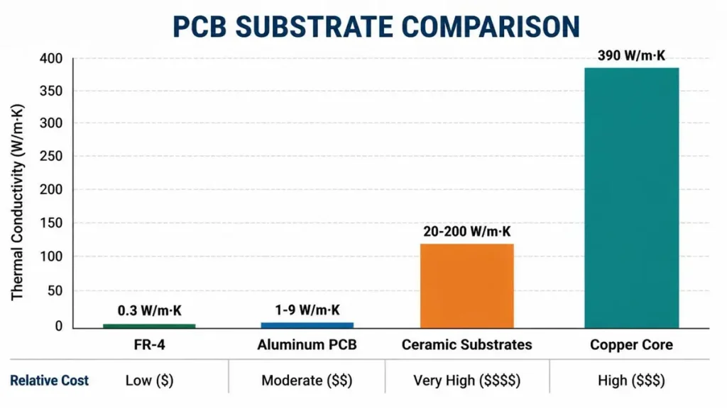
Thermal Conductivity (W/m.K) vs. Relative Cost Across Different PCB Substrates
The choice between an aluminum PCB board and other substrate families comes down to
three variables: thermal conductivity, cost, and mechanical rigidity.
1. FR-4 is inexpensive and easy to fabricate but has a thermal conductivity around 0.3
W/m·K, making it unsuitable for high-heat-flux components without added heat
spreaders.
2. Aluminum PCB / aluminum clad PCB typically reaches 1–9 W/m·K depending on the
dielectric formulation, at a fraction of the cost of copper-core boards.
3. Copper core PCB offers higher conductivity (around 390 W/m·K for the copper layer
itself) but adds significant weight and material cost, and is generally reserved for
extreme thermal loads.
4. Ceramic substrates (aluminum nitride, alumina) deliver the highest thermal
performance, often exceeding 20 W/m·K, but at a materials cost and brittleness trade
off that rules them out for many commercial programs.
For the majority of LED lighting, DC-DC power modules, motor drivers, and consumer
power electronics, an aluminum PCB manufacturer can hit the thermal target at a
substantially lower cost than copper or ceramic routes, which is why aluminum PCB boards
remain the default choice across these categories.
Typical Applications for Metal Core PCB and Aluminum Circuit Board Designs
1. LED lighting modules — street lighting, high-bay fixtures, automotive headlamps and
tail lamps
2.Power supply and power conversion boards — AC-DC converters, DC-DC regulators,
battery management systems
3. Automotive electronics — engine control modules, motor controllers, EV onboard
chargers
4.Industrial motor drives and solid-state relays
5.RF power amplifiers and audio amplifier output stages
The common thread across these applications is a concentrated heat source — an LED die, a
MOSFET, an IGBT — that needs a low-resistance thermal path built directly into the board
rather than relying solely on external heatsinking
Aluminum PCB Structure and Material Composition
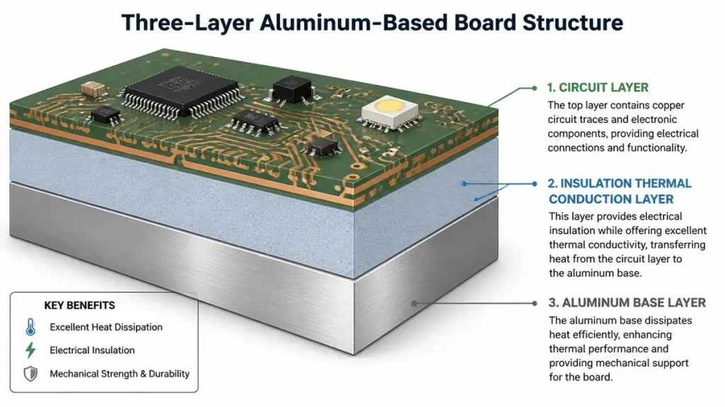
Exploded Cross-Section View of a Standard Three-Layer Aluminum PCB Board.
An aluminum PCB board is built from three functional layers bonded together under heat
and pressure:
- Circuit layer — electrolytic copper foil, patterned into the conductive traces and pads.
- Dielectric (insulation) layer — a thermally conductive, electrically insulating resin,
typically a ceramic-filled epoxy, that bonds the copper layer to the metal base while
providing dielectric withstand voltage. - Metal base layer — the aluminum substrate itself, which serves as both mechanical
support and the primary heat-spreading path.
Aluminum Base Material Grades
Most aluminum PCB manufacturers work with 5052 or 6061 aluminum alloy for the base
layer, chosen for a balance of thermal conductivity, mechanical stiffness, and cost. 5052 is
more common in general-purpose LED and power applications, while 6061 is sometimes
specified where higher mechanical strength or better machinability is required for
mounting and enclosure integration.
Dielectric Layer: The Layer That Actually Controls Thermal Performance
The dielectric layer, not the aluminum itself, is usually the limiting factor in an aluminum
PCB’s thermal resistance. Standard dielectric formulations run 1.0–3.0 W/m·K; high
performance ceramic-filled dielectrics used in premium metal core PCB stacks can reach 6
9 W/m·K, at a proportionally higher material cost. Dielectric thickness is typically specified
between 75µm and 150µm (0.003″–0.006″): thinner dielectric layers improve thermal
transfer but reduce dielectric breakdown voltage, so the specification has to be matched to
the application’s isolation voltage requirement, not chosen purely to minimize thermal
resistance.
Surface Finish Options for Aluminum Circuit Board Assemblies
1. HASL (Hot Air Solder Leveling) — cost-effective, suited to through-hole and simpler SMT layouts
2. ENIG (Electroless Nickel Immersion Gold) — flat surface, good for fine-pitch SMT and wire-bonded LED packages
3.OSP (Organic Solderability Preservative) — lower cost, shorter shelf life, common on high-volume LED boards
4.Immersion Silver / Immersion Tin — used selectively where RF performance or specific soldering profiles are required
Core Parameters and Manufacturability Range for Aluminum PCB Board Fabrication
| Capability Item | Standard Capability | Advanced / Custom Capability |
| Layer Count | 1 – 2 Layers | Multilayer Aluminum PCB / Copper-Aluminum Composite (Up to 4-6 Layers) |
| Base Material Type | 1060 / 5052 / 6061 Aluminum | High-Thermal Special Aluminum Alloy, Copper Base |
| Dielectric Thermal Conductivity | 1.0, 1.5, 2.0 W/m.K | 3.0, 4.0, 5.0, 8.0 W/m.K (Nano-Ceramic Filled) |
| Finished Board Thickness | 0.6mm – 2.0mm | 0.4mm – 4.0mm |
| Aluminum Base Thickness | 0.5mm – 1.5mm | 0.3mm – 3.5mm |
| Outer Copper Weight | 1oz – 3oz | 3oz – 10oz (Heavy Copper Process) |
| Min. Line Width / Spacing | 4/4 mil (0.10/0.10mm) | 3/3 mil (0.075/0.075mm) |
| Min. Finished Hole Size | 0.3mm | 0.15mm (Laser Drilling Available) |
| Solder Mask Color | High-Reflective White, Glossy Black | Matte White, Matte Black, Green, Blue, Red, Yellow |
| Surface Finish | LF HASL (Lead-Free Hot Air Solder Leveling), OSP | ENIG (Electroless Nickel Immersion Gold), Immersion Silver |
| Breakdown / Withstand Voltage | More than 2000V AC | More than 4000V / 6000V AC (High Insulation) |
| Thermal Shock Test | 288 Degrees Celsius, 3 times | 288 Degrees Celsius, 10 min (No Delamination, No Blistering) |
| Outline & Profiling | Punching, V-Scoring (V-Cut), CNC Routing | Controlled Depth Milling (Cavity), Countersunk / Counterbored Holes |
Manufacturability Notes Procurement Teams Should Confirm Before Ordering
1. Heavier copper weights (4 oz and above) require adjusted etch compensation and
impact minimum achievable trace width — confirm this before finalizing a layout
intended for high-current traces.
2. Aluminum PCB boards do not support standard multilayer via-in-pad plating the
same way FR-4 does; thermal vias and via structures need to be reviewed by
engineering rather than copied directly from an FR-4 design.
3. Solder mask and legend printing on aluminum substrates can show more color
variation near panel edges due to the metal base’s heat dissipation during the curing
step — this is a cosmetic, not functional, consideration but is worth flagging with your
supplier if consistent finish appearance matters for a visible LED module.
4. Panelization strategy affects both routing and thermal performance; aluminum
panels are stiffer than FR-4 and change how depaneling should be planned (V-scoring
versus routing with tabs).
Aluminum PCB Manufacturing Process: From Engineering Review to Finished Board
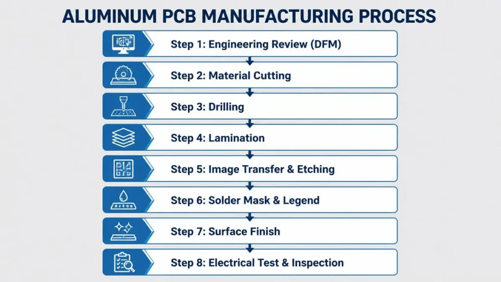
Comprehensive Manufacturing Process Flowchart for High-Reliability Aluminum PCBs
A disciplined aluminum PCB manufacturing process reduces the risk of delamination,
warping, or thermal layer failure — the three defect modes most specific to metal-core
boards.
Step 1: Data and Engineering Review (DFM)
Gerber files, drill files, and stack-up requirements are checked against the target application’s thermal and electrical requirements before any material is cut. This is the stage where trace width for current-carrying capacity, dielectric thickness for isolation voltage, and copper weight for thermal spreading are cross-checked.
Step 2: Material Cutting and Base Preparation
Aluminum sheet stock is cut to panel size, and the surface is prepared to ensure proper adhesion of the dielectric layer during lamination.
Step 3: Drilling
Mechanical or laser drilling forms the mounting holes and any through-board vias. Drill
parameters differ from FR-4 due to the aluminum base’s mechanical properties — feed rate
and bit selection are adjusted to avoid burring at the aluminum-dielectric interface.
Step 4: Lamination / Pressing
The copper foil, dielectric layer, and aluminum base are bonded under controlled heat and
pressure. This step determines the board’s final thermal resistance and bond strength, and
is the most quality-critical stage in aluminum PCB production.
Step 5: Image Transfer and Etching
The circuit pattern is transferred onto the copper layer using photoresist and exposure,
followed by etching to remove unwanted copper and define the final trace geometry.
Step 6: Solder Mask and Legend Printing
Solder mask is applied and cured, followed by legend (silkscreen) printing for component
reference designators.
Step 7: Surface Finish
HASL, ENIG, OSP, or immersion finishes are applied depending on the assembly and
soldering requirements specified by the customer.
Step 8: Electrical Test and Inspection
Every panel is electrically tested, and dimensional and cosmetic inspection is performed
prior to packaging.
Step 9: 2026 Manufacturing Technology Additions
Aluminum PCB fabrication in 2026 increasingly incorporates process technology that was
previously reserved for high-reliability multilayer boards:
1. AI-assisted automated optical inspection (AOI): deep-learning-based defect
classification now distinguishes cosmetic dielectric bleed-out from functional
delamination risk, reducing false-reject rates on metal-core panels compared to rule
based AOI systems.
2, Laser direct imaging (LDI): increasingly applied to aluminum PCB circuit layers to
hold tighter line-width tolerance for LED driver and power-density-critical layouts,
replacing older phototool-based exposure on higher-spec jobs.
3.Advanced ceramic-filled dielectric compounds: newer resin systems push thermal
conductivity higher without sacrificing dielectric breakdown voltage, closing part of
the performance gap with copper-core boards for mid-power applications.
4. Halogen-free and low-VOC dielectric and solder mask materials: driven by both
regulatory pressure and OEM sustainability requirements, particularly for automotive
and European-market programs.
5. Inline thermal-resistance sampling: statistical sampling of thermal resistance per
production lot, rather than only at initial qualification, is becoming a standard quality
gate for automotive-grade aluminum PCB manufacturers.
How to Select the Right Aluminum PCB Board for Your Application
When a Single-Layer Aluminum PCB Is Sufficient
Single-layer aluminum PCB boards are the right fit when the circuit is relatively simple,
component density is moderate, and the primary requirement is heat spreading from one
side of the board — this covers the large majority of LED lighting and single-stage power
converter designs.
When to Consider Multilayer or Higher-Conductivity Aluminum PCB Structures
Designs that require routing on both sides, higher component density, or heat sources on
multiple areas of the board may need a multilayer aluminum PCB or a hybrid stack
combining an aluminum base with additional dielectric and copper layers. Applications
with very high power density — EV onboard chargers, high-power LED arrays, or industrial
motor drives — often justify the added cost of a higher-thermal-conductivity dielectric
even on a single-layer structure.
Eight Details Procurement Should Confirm Before Requesting a Quote
Eight Details Procurement Should Confirm Before Requesting a Quote
- End application and expected operating environment (indoor, outdoor, automotive
under-hood, etc.) - Power dissipation and heat source location on the board
- Required copper weight for current-carrying traces
- Aluminum base thickness and any mechanical mounting constraints
- Required thermal conductivity of the dielectric layer
- Surface finish compatible with the intended assembly process
- Certification requirements (UL, IATF 16949, RoHS, REACH)
- Order volume and expected reorder cadence, since tooling and panel utilization are
optimized differently for prototype versus production quantities
Common Ordering Mistakes When Sourcing Aluminum PCB Boards
1. Specifying a thinner dielectric purely to reduce cost without checking the isolation
voltage requirement of the application
2. Reusing an FR-4 via and thermal pad layout directly on an aluminum PCB design
without engineering review
3. Underspecifying copper weight for high-current traces, leading to excessive trace
heating independent of the base’s thermal conductivity
4. Failing to confirm panel utilization and depaneling method early, which affects unit
cost more than most buyers expect
Comparing Aluminum PCB Manufacturers: What Actually Differentiates Suppliers
1. Engineering support — whether DFM review happens before tooling, or only after a
failed first article
2. Lead time transparency — realistic prototype and volume lead times, not just quoted
best-case numbers
3. Certifications — ISO 9001 as a baseline, IATF 16949 for automotive programs, UL
recognition where required
4. Batch-to-batch consistency — thermal resistance and dielectric thickness
consistency across production lots, not just the first qualification sample
Manufacturing Capabilities at Shenzhen Hongda Circuit Technology
Shenzhen Hongda Circuit Technology Co., Ltd. supports aluminum PCB programs from
initial prototype through sustained volume production, with in-house engineering review
on every incoming job.
1. Panel size range: production capability up to large-format panels, with engineering
support for panelization optimization on both prototype and volume orders
2. Lead time: prototype turnaround measured in days rather than weeks for standard
aluminum PCB board stack-ups, with volume scheduling built around confirmed
forecast and reorder cadence
3. Prototype-to-production transition: the same engineering team that reviews a first
article prototype carries the design through to volume tooling, reducing the risk of a
design passing prototype validation but failing at scale
4. Quality systems: ISO 9001 certified manufacturing, with IATF 16949 process controls
applied to automotive-designated programs
5. Test and inspection capability: electrical test on 100% of production, AOI on circuit
layers, and dimensional inspection aligned to customer drawing requirements
6. Industry experience: production history across LED lighting modules, automotive
power electronics, and industrial power supply boards, with application engineering
support available during the quoting stage
Design for Manufacturability (DFM) Guidance for Aluminum PCB Layouts
Thermal Management Design Considerations
Place high-power components directly over thermal vias or thermal pads connected to the
aluminum base rather than routing heat through copper traces alone. Where possible, keep
the highest-power components toward the center of the board rather than the edge, since
edge components have a shorter thermal path but also experience more temperature
variation during reflow.
Trace, Copper Pour, and Via Design Limits
1. Match copper weight to the current-carrying requirement first, then check that
minimum trace width and spacing are achievable at that copper weight
2. Avoid unnecessarily narrow traces on high-current nets; the aluminum base does not
compensate for undersized copper cross-section
3. Confirm solder mask opening size around thermal pads with your aluminum PCB
manufacturer, since mask registration tolerance differs slightly from FR-4 boards
Recommendations for High-Power and High-Reliability Programs
For automotive-grade and other high-reliability aluminum PCB programs, request thermal
resistance test data from the specific dielectric and copper-weight combination being used,
rather than relying on generic datasheet values for the dielectric material alone. Confirm
CTE (coefficient of thermal expansion) compatibility between the aluminum base and any
surface-mount components with large body size, since thermal cycling stress on solder
joints is a more common field-failure mode on metal-core boards than on FR-4.
Frequently Asked Questions About Aluminum PCB
How do I verify that an aluminum PCB manufacturer’s quoted thermal conductivity is accurate?
Ask for the actual test report or datasheet from the dielectric material supplier, not just a marketing figure, and confirm whether the number quoted applies to the dielectric layer alone or the full stack.
What certifications should I require before qualifying a new aluminum PCB supplier?
At minimum, ISO 9001; for automotive or safety-critical programs, IATF 16949; and UL recognition where the end product requires it. Ask to see the certificate and confirm scope, not just the certification name.
How do I compare lead times fairly across different aluminum PCB manufacturers?
Request lead time quotes for both prototype and volume quantities separately, and ask whether the quoted lead time starts from data approval or from material availability, since suppliers define this differently.
What is a reasonable way to evaluate sample quality before committing to a production order?
Request a first-article inspection report alongside the physical samples,
including dimensional measurements, thermal resistance test data if available, and cross section images of the dielectric bond line.
How should I structure an RFQ to get accurate aluminum PCB board pricing?
Include the full stack-up (base thickness, dielectric thermal conductivity, copper weight), surface finish, panel utilization preference, quantity break points, and any certification requirements — incomplete RFQs are the most common reason quoted prices vary widely between suppliers for what buyers assume is the same board.
Shenzhen Hongda Circuit Technology Co., Ltd. specializes in quick-turn and mass production of high-performance Aluminum PCBs, fully optimized for 2026 AI power supplies and automotive electronics. For tailored specifications or instant RFQ, please contact our engineering team directly at sales@pcbkr.com
About Author
David Chen https://www.linkedin.com/in/pcbcoming
David Chen boasts an extensive professional background in PCBA manufacturing, PCBA testing, and PCBA optimization, with specialized expertise in high-precision PCBA fault analysis and rigorous PCBA reliability testing. The author has worked with high-layer-count server PCB fabrication, ultra-low-loss backplane stackups, and thermo-mechanical reliability optimization for AI infrastructure projects involving 112G and 224G PAM4 architectures. Skilled in complex circuit design and cutting-edge advanced PCB manufacturing processes, he delivers solutions that elevate product durability and performance across industrial applications. His technical articles focusing on PCBA manufacturing workflows and testing methodologies are widely cited by industry peers, research institutions, and technical platforms, solidifying his reputation as a recognized technical authority in the global circuit board manufacturing sector.