Gold Finger PCB: Core Applications, Manufacturing Excellence & Industry Solutions
PCB Gold fingers edge connector: Why Gold Finger PCB Technology Defines Modern Interconnect Reliability
A gold finger PCB—also referred to as an edge connector PCB or electroplated gold PCB—is not merely a surface finish choice. It is a mission-critical interface engineering decision. The gold-plated contact pads running along the board edge serve as the primary electrical and mechanical bridge between a daughter card and its host system, whether that is a motherboard backplane, a GPU accelerator slot, or an industrial control rack.
In 2026, the demands placed on PCB gold finger technology have intensified dramatically. With PCIe Gen 5 (32 GT/s) and Gen 6 (64 GT/s) architectures pushing signal integrity to its theoretical limits, AI server backplanes requiring 224G PAM4 transmission, and automotive modules facing ISO 26262 functional safety mandates, the margin for connector failure has effectively shrunk to zero. A substandard gold finger—whether compromised by insufficient plating thickness, improper nickel underplate, or missing edge beveling—can cascade into system-level failures that cost millions in downtime and field recalls.
At Shenzhen Hongda Circuit Technology Co., Ltd. (PCBkr), we manufacture gold finger PCBs that bridge the gap between cutting-edge performance and industrial-grade reliability. Our facility in Shenzhen operates with IPC-6012 Class 3/3A and AS9100D aerospace certifications, delivering selective hard gold plating with thickness control from 10 μin to 100 μin, precision beveling at ±2° tolerance, and impedance-matched finger layouts verified through 100% electrical testing. This guide explains the real-world applications, technical specifications, and procurement criteria that hardware engineers and supply chain managers need to evaluate in 2026.
PCB Gold fingers edge connector Applications Across High-Performance Computing & Critical Infrastructure
PCIe Gold Finger PCB for High-Speed Expansion Slots (Gen 5 & Gen 6)
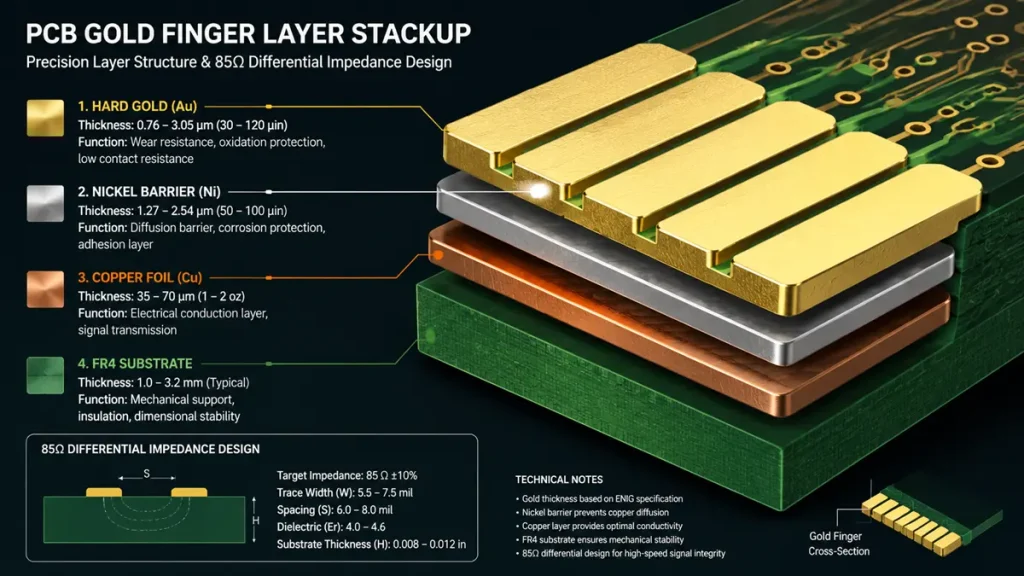
Cross-sectional 3D layer stackup and 85Ω differential impedance parameters for high-speed PCB gold fingers.
The PCIe gold finger PCB represents one of the most technically demanding edge connector implementations in consumer and enterprise hardware. As PCI Express evolves from Gen 4 (16 GT/s) to Gen 5 (32 GT/s) and the emerging Gen 6 (64 GT/s), the signal integrity budget at the connector interface has tightened to unprecedented levels.
Key Engineering Challenges:
- Impedance Discontinuity: Gold finger pads must maintain controlled impedance—typically 85 Ω differential for PCIe lanes. The additional copper and nickel buildup from electroplating (approximately 5 μm per side) reduces effective spacing between adjacent fingers. Without pre-compensation in the Gerber layout, this plating buildup can shift impedance by 1–3 Ω, directly contributing to insertion loss and eye diagram closure.
- Intra-Pair Skew: Differential pairs within a lane require length matching to ±5 mil (±0.127 mm) at the finger area. Any pad length asymmetry translates into skew that degrades signal quality at 32 GT/s and above.
- High-Cycle Durability: Server-grade PCIe cards in data centers may undergo hundreds of insertion cycles during burn-in, testing, and field maintenance. Standard 30 μin (0.76 μm) hard gold over 100 μin (2.54 μm) nickel provides adequate wear resistance for consumer applications, but enterprise backplanes often demand 50 μin (1.27 μm) Class 3 plating to survive 1,000+ cycles without contact resistance degradation.
At Shenzhen Hongda Circuit Technology, our PCIe gold finger PCB manufacturing process addresses these challenges through a multi-step engineering workflow. We use 2.5D field-solver impedance simulation to model the finger-to-connector interface before layout, compensating pad widths for expected plating buildup. Our SCREEN Ledia LDI exposure systems maintain ±5% differential impedance control, while selective hard gold plating—applied only to contact pads, never to solderable SMT areas—ensures solder joint reliability on the same board. For high-volume server builds, we validate every production lot with insertion/extraction cycle testing and contact resistance measurement across the full temperature range.
GPU Gold Finger PCB & Accelerator Card Edge Connectors
Graphics processing units (GPUs) and AI accelerator cards present a unique intersection of challenges for gold finger PCB design: extreme power delivery, massive data throughput, and thermal cycling that stresses both the substrate and the connector interface.
Modern AI accelerators draw 600W to 700W through the PCIe slot and auxiliary power connectors. The gold fingers responsible for 12V power delivery must carry sustained currents without excessive resistive heating. This requires not only adequate finger width and copper thickness but also optimized nickel underplate thickness (150–200 μin) to prevent current crowding and localized heating at the contact interface.
Hongda’s Technical Approach:
Our GPU gold finger PCB production line supports heavy copper configurations up to 6 oz outer layer copper, with selective hard gold plating graded by current-carrying requirements. For AI training clusters where accelerator cards are swapped frequently during maintenance windows, we offer 50 μin Class 3 hard gold with cobalt-hardened alloy (0.3–0.5% Co) achieving 170–200 HK Knoop hardness. Post-plating polishing to Ra <0.4 μm reduces the friction coefficient during insertion, extending connector life and minimizing gold debris accumulation in the mating socket.
AI Server Gold Finger PCB for 224G PAM4 Backplanes & UBB Modules

High-density gold finger edge connector applied in 224G PAM4 AI server backplane and accelerator modules.
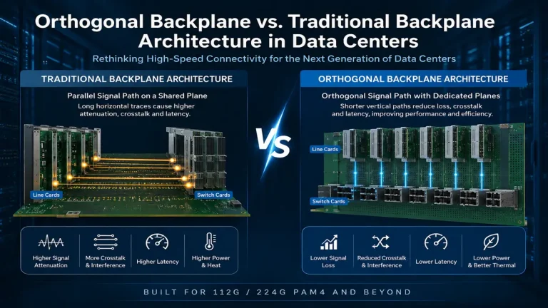
The AI infrastructure boom has redefined what a gold finger PCB must accomplish. In universal baseboard (UBB) architectures and orthogonal backplanes supporting 224G PAM4 signaling, the edge connector is no longer just a power and low-speed data interface—it is a high-speed transmission line stub that must preserve signal integrity across 56 GHz of effective bandwidth.
Critical Specifications for AI Server Gold Fingers:
- Material Stackup: Low-loss laminates such as Panasonic Megtron 7 (Dk 3.37, Df 0.0020) or Isola Tachyon 100G are standard for high-speed signal layers. However, the gold finger area itself introduces a material discontinuity (gold over nickel over copper) that must be modeled as part of the channel simulation.
- Backdrilling & Stub Control: In multilayer backplanes (up to 104 layers in Hongda’s capability), through-hole vias near gold fingers create stub resonance. Our backdrilling process achieves ±0.05 mm depth tolerance, eliminating unused via barrel sections that would otherwise cause quarter-wave resonance at 28 GHz.
- Thermal & Mechanical Stress: AI server nodes operate at elevated temperatures (60–85 °C ambient at the board edge). Thermal cycling induces differential expansion between the gold layer, nickel barrier, and copper pad. Hongda’s plating process includes a proprietary thermal shock qualification (–40 °C to +125 °C, 1,000 cycles) to verify that no micro-cracking or delamination occurs at the finger edge.
Our facility has shipped gold finger PCBs for AI server OAM modules, UBB motherboards, and high-speed switch boards since 2024, with production processes validated for 112G and 224G PAM4 architectures.
DDR5 Memory Module Gold Finger PCB Design & Signal Integrity
DDR5 memory modules operate at data rates up to 6,400 MT/s (with overclocked variants exceeding 8,400 MT/s), introducing signal integrity challenges that previous generations rarely faced. The DDR5 gold finger PCB must manage higher signal frequencies, tighter noise margins, and more complex on-die termination schemes than DDR4.
Technical Implementation:
- JEDEC MO-002 Compliance: DDR5 DIMM gold fingers follow strict dimensional and plating specifications. Standard gold thickness ranges from 0.76 μm to 1.27 μm (30–50 μin) over a 3–6 μm nickel barrier, with finger pitch and length tightly controlled to ensure compatibility across motherboard slots from different vendors.
- Crosstalk Mitigation: At DDR5 speeds, capacitive coupling between adjacent gold fingers can induce near-end crosstalk (NEXT). Hongda’s design rule checks (DRC) enforce minimum spacing algorithms that account for plating thickness buildup, while our impedance testing verifies that each finger pair meets the target specification before shipment.
- Beveling for Hot-Swap Durability: Server memory is frequently replaced in the field. A 30° or 45° chamfer on the leading edge of the DIMM ensures smooth insertion into latching sockets without damaging the gold plating or the socket’s contact beams. Our CNC beveling equipment maintains ±2° angular accuracy with no burr or fiber exposure.
Storage Module Gold Finger PCB for NVMe & SSD Edge Connectors
Solid-state drives (SSDs) and NVMe modules rely on gold finger PCBs for both PCIe signal routing and power delivery in ultra-compact form factors (M.2 2230/2242/2280, U.2, E1.S, E3.S). The primary failure mode in storage applications is not typically wear-through of the gold layer—since consumer SSDs rarely exceed 50 insertion cycles—but rather contact fretting corrosion caused by micro-motion vibration in laptop and automotive environments.
Hongda’s Solution for Storage Applications:
We offer dual-surface-finish boards that combine hard gold fingers (30 μin) with ENIG or OSP on component solder pads. The manufacturing sequence—solder mask application, selective plating resist, ENIG/OSP on SMT areas, resist stripping, and final selective hard gold on fingers—ensures that no cobalt or nickel alloying elements from the hard gold process contaminate solderable surfaces. For industrial and automotive SSDs, we provide thicker 50 μin gold with enhanced nickel underplates (200 μin) to resist fretting corrosion under sustained vibration.
Industrial, Automotive & Mission-Critical Gold Finger PCB Applications
Industrial Control Gold Finger PCB for Harsh Environment Reliability
Industrial automation systems—PLCs, I/O modules, motor drives, and robotic controllers—operate in environments characterized by vibration, dust, humidity, and temperature swings from –40 °C to +85 °C. In these conditions, a standard 30 μin gold finger PCB may not provide sufficient protection against corrosion-induced contact resistance increase.
Engineering Specifications for Industrial Gold Fingers:
- Thick Hard Gold: 50 μin (1.27 μm) Class 3 plating is standard for industrial backplanes and rack-mounted I/O cards. For extreme environments (offshore oil & gas, mining), 100 μin (2.54 μm) gold over 200 μin (5.08 μm) nickel provides a wear life exceeding 10,000 insertion cycles.
- Edge Plating & Beveling: Some industrial designs require edge plating (plated board edge) in addition to gold fingers, providing EMI shielding and ground continuity. Hongda’s process supports selective edge plating with subsequent beveling, maintaining plating integrity at the chamfer transition.
- Conformal Coating Compatibility: When boards require conformal coating (acrylic, urethane, or silicone), the solder mask clearance around gold fingers must be precisely defined to prevent coating creep onto contact surfaces. Our DFM team reviews every industrial design for coating keepout zones before production.
Automotive Gold Finger PCB for EV Powertrain & ADAS Modules
The automotive electronics sector imposes some of the most stringent reliability requirements on gold finger PCBs. Under IATF 16949 and evolving ISO 26262 functional safety standards, connector failures in battery management systems (BMS), onboard charging modules, or ADAS sensor hubs can have catastrophic consequences.
Automotive-Specific Gold Finger Challenges:
- Thermal Stability: Under-hood temperatures can reach 125 °C continuous (150 °C peak). Standard cobalt-hardened gold can experience grain boundary changes at these temperatures, potentially increasing contact resistance. Hongda offers high-temperature-qualified plating chemistries with optimized cobalt content (0.1–0.3%) that maintain stable resistivity through 1,000 hours at 150 °C.
- Vibration Resistance: EV powertrain modules experience severe vibration (ISO 16750-3, Test VII). Our automotive gold finger PCBs undergo random vibration testing (5–2,000 Hz, 8 Grms) followed by contact resistance verification to ensure no fretting degradation occurs.
- Humidity & Salt Spray: For modules exposed to underbody splash or coastal environments, we apply 100-hour salt spray testing (ASTM B117) as a standard qualification step for automotive gold finger designs.
Medical Device Gold Finger PCB for Diagnostic & Monitoring Equipment
Medical electronics demand zero-defect reliability combined with biocompatibility and chemical resistance. Diagnostic imaging systems (MRI, CT), patient monitors, and portable ultrasound devices use gold finger PCBs for modular sub-assemblies that must be swapped quickly during critical procedures.
Hongda’s Medical Gold Finger Capabilities:
Certified to ISO 13485 medical device quality standards, we manufacture gold finger PCBs with:
- High-purity Type I gold (99.9%) for applications requiring biocompatibility and minimal alloying element exposure
- Traceable plating chemistry with full material declaration (RoHS, REACH) for regulatory submissions
- 100% automated optical inspection (AOI) of finger geometry, spacing, and plating coverage
- Cross-sectional analysis on first articles to verify nickel barrier integrity and gold thickness uniformity
Aerospace & Defense Gold Finger PCB for Extreme Environment Survival
Aerospace and defense applications—satellite communications, avionics, radar systems, and missile guidance—push gold finger PCB technology to its absolute limits. These boards must survive extreme temperatures (–55 °C to +125 °C), high-altitude radiation, and severe mechanical shock (MIL-STD-810).
Military-Grade Gold Finger Specifications:
- MIL-DTL-45204D Compliance: Aerospace applications typically require Class 2 or higher (0.0002 inches / 5 μm minimum) gold thickness per military specification.
- ASTM B488 Type II: Gold-cobalt alloy (0.3–0.5% Co) with nickel underplating provides the hardness and wear resistance needed for military connectors.
- Outgassing Control: For vacuum environments (spacecraft), plating chemistries must meet NASA outgassing requirements (ASTM E595). Hongda maintains qualified material lists (QML) for aerospace plating processes with full outgassing test reports.
Our AS9100D-certified production line supports 60+ layer backplanes and rigid-flex assemblies with gold fingers, delivering the documentation traceability (material certs, process travelers, test reports) required for defense prime contractor audits.
5G Telecommunications & Network Equipment Gold Finger PCB
5G base stations, core routers, and optical transport platforms operate at microwave frequencies where every millimeter of transmission path matters. The gold finger PCB in a 400G/800G optical module or a 5G massive MIMO antenna card must preserve signal integrity while surviving years of outdoor exposure.
Technical Focus Areas:
- Low-Loss Material Integration: We combine gold finger plating with Rogers RO4350B, Taconic TLY-5, and Panasonic Megtron 6 substrates to minimize dielectric loss at 28 GHz and 39 GHz 5G bands.
- Anti-Corrosion Design: Outdoor telecom equipment faces sulfur-rich urban atmospheres that can tarnish gold surfaces over time. Our 50 μin+ hard gold with dense, pore-free nickel barriers (verified by sulfur porosity testing) ensures 15+ year field life.
- Precision Micro-Board Edge Routing: For compact SFP, QSFP, and OSFP optical modules, gold fingers are often located on extremely thin board edges (0.8 mm or less). Hongda’s profiling equipment maintains ±0.05 mm board edge tolerance, ensuring proper connector mating without mechanical interference.
Gold Finger PCB Manufacturing Process, Specifications & Quality Control
Hard Gold Plating vs. ENIG: Why Electroplated Gold Is Non-Negotiable for Edge Connectors
A common misconception in PCB manufacturing is that all gold finishes are interchangeable. This is dangerously incorrect for gold finger applications.
Electroplated Hard Gold (The Only Choice for Fingers):
- Composition: 98% pure gold alloyed with 0.1–0.5% cobalt or nickel for hardness
- Knoop Hardness: 130–200 HK (vs. ~60 HK for soft gold)
- Thickness Range: 10 μin to 100 μin (0.25 μm to 2.54 μm), selectable by application class
- Wear Resistance: 1,000 to 10,000+ insertion cycles depending on thickness
- Contact Resistance: <1 mΩ stable across cycle life
ENIG (Electroless Nickel Immersion Gold):
- Composition: 99.9% pure soft gold, 2–5 μin thick
- Hardness: Too soft for sliding contacts; wears away in <100 cycles
- Use Case: SMT pad surface finish only—never for edge connectors
Critical Design Rule: Never specify hard gold on SMT pads or through-holes. The cobalt/nickel alloying elements will compromise solder joint reliability, potentially causing embrittlement if gold exceeds 3% by mass in the solder joint. Always use selective plating: hard gold on fingers, ENIG or OSP on solderable areas.
Nickel Underplate: The Hidden Barrier That Determines Gold Finger Lifespan
The nickel layer beneath the gold is not merely a substrate—it is the primary diffusion barrier preventing copper migration into the gold, and it provides the mechanical wear surface that supports the gold layer under contact pressure.
Nickel Underplate Specifications:
| Parameter | Standard Spec | High-Reliability Spec | Critical Application |
| Thickness | 100 μin (2.5 μm) | 150 μin (3.8 μm) | 200–250 μin (5–6.35 μm) |
| Purpose | Basic diffusion barrier | Enhanced wear resistance | Maximum cycle life |
| Applications | Consumer electronics | Industrial, medical | Aerospace, test fixtures |
At Hongda, we verify nickel thickness on every production panel using XRF (X-ray fluorescence) spectrometry, with statistical process control (SPC) charts tracking thickness uniformity across the panel. Variations exceeding ±10% trigger automatic process adjustment.
Gold Finger Beveling (Chamfering) Process: Angles, Tolerances & DFM
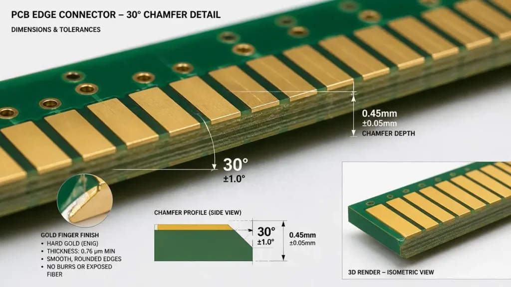
Engineering measurement parameters for PCB gold finger 30° beveling chamfer angle (±1.0°) and chamfer depth tolerances.
PCB gold finger beveling is a mechanical finishing process that transforms the sharp 90° board edge into an angled ramp (typically 20° to 45°), allowing smooth insertion into the mating connector without damaging contact pins or the gold plating itself.
Standard Beveling Specifications:
- Angle: 30° (most common), 45° (heavy-duty/industrial), 20° (minimal insertion assistance)
- Depth: 0.5–1.5 mm from board edge
- Tolerance: ±2° angle accuracy
- Surface Finish: Burr-free, no fiber exposure, smooth transition across plated edge
Manufacturing Sequence at Hongda:
- Panel Routing: CNC profiling defines the board outline
- Nickel & Hard Gold Plating: Electroplating applied to finger areas
- Solder Mask Application: Mask carefully avoids gold finger zones (minimum 0.5–1.0 mm clearance)
- Beveling: CNC-controlled precision grinding with selective angle capability (different edges, different angles)
- Cleaning & Inspection: Debris removal, optical angle verification, plating integrity check
DFM Tip: Always specify the bevel angle in your fabrication notes and mechanical layer. For boards with gold fingers on multiple edges (e.g., some memory modules), confirm that your manufacturer supports selective beveling—Hongda’s equipment handles complex multi-angle profiles in a single setup.
Gold Finger PCB Thickness Classes & Cycle Life Ratings
Understanding gold finger PCB thickness requirements is essential for cost optimization without over-engineering. The IPC and ASTM standards define practical classes:
| Class | Gold Thickness | Typical Use Case | Cycle Life |
| Class 1 | 10–15 μin | Prototypes, limited mating | <500 |
| Class 2 | 30 μin | Standard edge connectors, consumer GPU, DDR | 500–1,000 |
| Class 3 | 50 μin | Industrial, server, medical | 1,000–5,000 |
| Class 4+ | 75–100 μin | Aerospace, test fixtures, high-cycle | 5,000–10,000+ |
Cost Impact: Moving from Class 2 (30 μin) to Class 3 (50 μin) increases gold material cost by approximately 40–60%. However, for applications requiring 1,000+ cycles, the incremental plating cost is negligible compared to the total cost of ownership (TCO) of field failures and connector replacement.
Hongda provides transparent quoting that separates selective gold finger plating from base PCB costs, allowing procurement teams to optimize specifications precisely.
How to Choose a Gold Finger PCB Manufacturer: 2026 Procurement Checklist
Selecting a gold finger PCB supplier is not a commodity decision. The plating process, inspection rigor, and material traceability directly impact your product’s field reliability and brand reputation.
Technical Capability Verification
Before issuing a PO, verify that your gold finger PCB manufacturer can demonstrate:
- Selective Plating Equipment: Automated plating lines with photoresist masking capability, ensuring hard gold is applied only to fingers and never to solderable SMT pads
- XRF Thickness Verification: Non-destructive testing of gold and nickel thickness on every panel or statistically valid sampling
- Impedance Control: For high-speed fingers (PCIe, DDR5, 224G), confirm field-solver-based impedance modeling and ±5% tolerance achievement
- Beveling Precision: CNC equipment with ±2° tolerance and multi-angle selective capability
- Cross-Sectional Analysis: Microsection capability to verify plating adhesion, nickel barrier integrity, and absence of voids or cracks
Quality Certifications & Compliance
| Certification | Relevance to Gold Finger PCBs |
| IPC-6012 Class 3/3A | Rigid PCB performance qualification; Class 3A adds automotive requirements |
| IPC-4552 | Electroplated gold specifications for printed boards |
| ISO 9001:2026 | Quality management system baseline |
| AS9100D | Aerospace-specific quality requirements |
| ISO 13485 | Medical device quality standards |
| IATF 16949 | Automotive quality management |
| RoHS / REACH | Environmental compliance for global markets |
Shenzhen Hongda Circuit Technology holds IPC-6012 Class 3/3A, AS9100D, and ISO 13485 certifications, with full material declaration documentation for every production lot.
Material Ecosystem & Supply Chain Resilience
In 2025, global supply chain disruptions caused premium laminate lead times (e.g., Megtron 6) to spike from 4–6 weeks to 14–18 weeks. A forward-thinking gold finger PCB manufacturer must maintain:
- Qualified Alternative Material Lists: Pre-qualified substitute laminates for each product family to prevent production shutdowns
- Strategic Material Partnerships: Direct relationships with Tier-1 material suppliers (Isola, Panasonic, Rogers, Taconic)
- AI-Driven Inventory Management: Real-time ERP tracking with predictive reordering
Hongda’s 2026 material stock includes Megtron 7/8, RO4350B, RT5880, I-Tera MT40, and cost-optimized hybrid stackup options (premium materials on signal layers, standard FR-4 on power planes) that reduce material costs by 20–32% without performance compromise.
Engineering Support & DFM Collaboration
The most reliable gold finger PCBs are not manufactured—they are co-engineered. Look for a partner that provides:
- Pre-Layout DFM Review: Impedance stackup optimization, finger pad width compensation for plating buildup, bevel angle recommendations
- Fast-Turn Prototyping: 24-hour prototype capability for complex HDI gold finger designs
- 24/7 Technical Support: Direct engineering access, not ticket-based queues
- Full Documentation Package: Impedance reports, plating thickness certificates, cross-sectional photos, thermal cycle test data
At PCBkr, our engineering team—led by professionals with direct experience in 112G/224G PAM4 backplane design—provides 30-minute inquiry response, 1-hour RFQ triage, and 24/7 technical support via sales@pcbkr.com.
Frequently Asked Questions (FAQ) — Gold Finger PCB Procurement Guide
What is the difference between hard gold plating and ENIG for PCB gold fingers?
Hard gold plating is an electrolytic process that deposits a thick (30–100 μin), cobalt-hardened gold alloy directly onto a nickel underplate. It is the only suitable finish for gold finger PCBs because it withstands repeated insertion cycles (1,000–10,000+) with stable contact resistance. ENIG (Electroless Nickel Immersion Gold) deposits a thin (2–5 μin), soft gold layer intended for SMT solder pads. ENIG wears away in fewer than 100 insertion cycles and is never recommended for edge connectors. For boards requiring both gold fingers and SMT assembly, specify selective plating: hard gold on fingers, ENIG on pads.
How do I specify gold finger PCB plating thickness for my application?
Use a class-based approach: Class 2 (30 μin) for standard consumer and commercial applications with <1,000 insertion cycles; Class 3 (50 μin) for industrial, server, and medical devices requiring 1,000–5,000 cycles; and 75–100 μin for aerospace, defense, or test fixtures demanding 5,000+ cycles. Always pair gold thickness with an adequate nickel underplate (100–200 μin) to prevent copper diffusion and provide mechanical support. Your PCB manufacturer should verify thickness with XRF testing and provide certificates of conformance.
Why is gold finger beveling necessary, and what angle should I specify?
Beveling (chamfering) creates a tapered ramp on the leading edge of the PCB, reducing insertion force and preventing mechanical damage to both the gold plating and the connector’s contact pins. Without beveling, sharp 90° edges concentrate stress, causing premature gold depletion and potential connector pin bending. Specify 30° for most standard connectors, 45° for heavy-duty industrial or high-insertion-force applications, and 20° for minimal assistance designs. Always include bevel angle, depth, and tolerance (±2°) in your fabrication notes.
What is the difference between hard gold plating and ENIG for PCB gold fingers?
Use a class-based approach: Class 2 (30 μin) for standard consumer and commercial applications with <1,000 insertion cycles; Class 3 (50 μin) for industrial, server, and medical devices requiring 1,000–5,000 cycles; and 75–100 μin for aerospace, defense, or test fixtures demanding 5,000+ cycles. Always pair gold thickness with an adequate nickel underplate (100–200 μin) to prevent copper diffusion and provide mechanical support. Your PCB manufacturer should verify thickness with XRF testing and provide certificates of conformance.
What certifications should I look for when sourcing gold finger PCBs from China?
For mission-critical applications, verify IPC-6012 Class 3/3A (rigid PCB performance), IPC-4552 (electroplated gold specifications), and industry-specific certifications: AS9100D for aerospace, ISO 13485 for medical, and IATF 16949 for automotive. Additionally, confirm RoHS and REACH compliance for environmental regulations. Request factory audit access, cross-sectional analysis reports, and plating thickness verification data before committing to volume production. A transparent supplier will provide full material traceability and process documentation.
How does Shenzhen Hongda Circuit Technology ensure gold finger PCB reliability for high-speed applications like PCIe Gen 5 and AI servers?
Hongda addresses high-speed gold finger PCB reliability through a multi-layer engineering approach:
(1) Impedance pre-compensation using 2.5D field-solver modeling that accounts for plating buildup on finger pads;
(2) Tight process control with ±5% differential impedance tolerance, ±25 μm interlayer alignment, and 100% electrical testing;
(3) Advanced equipment including SCREEN Ledia LDI exposure, Mitsubishi laser drilling, and Nordson DAGE 3D X-Ray inspection;
(4) Material expertise with qualified low-loss laminates (Megtron 7, Tachyon 100G) and hybrid stackup optimization;
(5) Full validation testing including thermal cycling, insertion cycle simulation, and contact resistance measurement. Contact our engineering team at sales@pcbkr.com for a complimentary DFM review of your gold finger design.
Partner with Shenzhen Hongda Circuit Technology for Gold Finger PCB Excellence
The gold finger PCB is far more than a decorative gold strip on a board edge. It is a precision-engineered electromechanical interface whose design, plating, and geometry determine whether your product operates flawlessly for years or fails at the first insertion. From PCIe Gen 6 signal integrity to automotive vibration survival, from AI server 224G PAM4 channels to aerospace radiation hardness, every application demands a tailored approach to gold thickness, nickel barrier design, beveling geometry, and material selection.
At Shenzhen Hongda Circuit Technology Co., Ltd. (PCBkr), we combine 2026-leading manufacturing technology—mSAP fine-line processing, 224G backplane qualification, AI-driven quality inspection—with the agility and engineering responsiveness that tier-1 factories cannot match. Whether you need a prototype batch of DDR5 memory module PCBs or a volume production run of industrial backplanes with 50 μin hard gold, our team delivers zero-defect reliability without the premium overhead.
Ready to optimize your gold finger PCB design?
Submit your Gerber files and stackup requirements to sales@pcbkr.com today. Our engineering team will return a comprehensive DFM analysis, plating specification recommendation, and competitive quotation within 30 minutes.
About Author
David Chen https://www.linkedin.com/in/pcbcoming
David Chen boasts an extensive professional background in PCBA manufacturing, PCBA testing, and PCBA optimization, with specialized expertise in high-precision PCBA fault analysis and rigorous PCBA reliability testing. The author has worked with high-layer-count server PCB fabrication, ultra-low-loss backplane stackups, and thermo-mechanical reliability optimization for AI infrastructure projects involving 112G and 224G PAM4 architectures. Skilled in complex circuit design and cutting-edge advanced PCB manufacturing processes, he delivers solutions that elevate product durability and performance across industrial applications. His technical articles focusing on PCBA manufacturing workflows and testing methodologies are widely cited by industry peers, research institutions, and technical platforms, solidifying his reputation as a recognized technical authority in the global circuit board manufacturing sector.