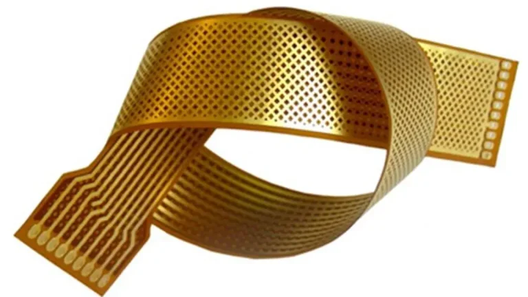
Sourcing High-Reliability Microvia PCBs from China: Supply Chain Guide for Global Procurement Teams
China microvias pcb manufacturer vetting is top‑of‑mind for procurement engineers and supply chain managers assessing China‑based HDI PCB partners. The question is no longer “Can they build it?”—it’s “Can they build it consistently, ship it compliantly, and support it globally?”
The New Geography of Microvia Manufacturing
In 2026, approximately 68% of advanced HDI and microvia PCB capacity is concentrated in the Pearl River Delta. This is not accidental. The ecosystem required to manufacture 104-layer backplanes with 20 μm laser-drilled microvias and mSAP fine-line circuits cannot be replicated overnight—it demands a dense network of laminate suppliers, plating chemistry providers, precision equipment vendors, and specialized logistics handlers operating within a 200-kilometer radius.
For global buyers sourcing AI server PCBs, automotive ADAS modules, or satellite communication payloads in High-Density Interconnect (HDI) Microvia PCB Manufacturing | mSAP & SAP Capabilities for AI Server and HPC Applications, China is not merely a low-cost option. It is often the only option for builds requiring Any-Layer HDI, copper-filled stacked microvias, and 224G PAM4 signal integrity qualification at production scale.
But geographic concentration creates a paradox: the same ecosystem that enables technological capability also introduces supply chain complexity—customs regulations, export control classifications, language barriers, and quality consistency across international distances.
This guide addresses how to navigate that complexity.
What “Reliable” Means in Microvia Supply Chain Context
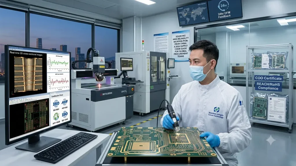
China Microvia PCB Manufacturer – High-Precision HDI PCB Inspection and Laser Drilling Facility
When evaluating a china microvias pcb manufacturer, procurement teams typically over-index on equipment lists and under-index on supply chain resilience. A supplier with Mitsubishi UV/CO₂ laser drills and SCREEN Ledia LDI systems is technically capable. But capability without supply chain reliability is a prototype shop, not a production partner.
Reliability in this context has four dimensions:
1. Process Consistency at Distance
High-Density Interconnect (HDI) Microvia PCB Manufacturing quality is statistically sensitive. A 2 μm shift in laser drill positioning or a 5% variation in copper plating thickness can mean the difference between a board that passes IST thermal cycling and one that fails after 500 hours in an AI server rack.
A reliable supplier must demonstrate:
- SPC (Statistical Process Control) with automated data collection across lamination, drilling, and plating—not manual logbooks
- Lot traceability from raw laminate reel to finished PCB serial number
- Microsection archives retained for the full product lifecycle, accessible via customer portal
At Shenzhen Hongda Circuit Technology, our AI-driven ERP tracks every panel by barcode through 40+ process steps. For aerospace and medical clients, we provide full material certification packages with DSC, TMA, and Dk/Df test data per laminate lot—not generic datasheets.
2. Logistics Architecture for Time-Critical Builds
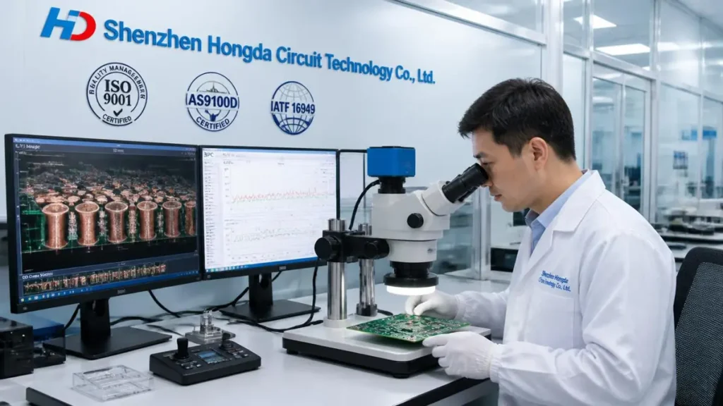
Shenzhen Hongda Circuit Technology Co., Ltd. – Microvia PCB Quality Control & Microsection Analysis Lab
AI server development cycles do not tolerate 25-day ocean freight delays for prototype iterations, our multi-tier fast turn solution is detailed in Custom Microvia PCB Fabrication & Quick-Turn HDI Prototyping: A 2026 Procurement Decision Framework. A global-ready microvia supplier must maintain:
- Multi-modal shipping: Air freight for prototypes (48-hour to 5-day turnaround), sea freight for volume, and express courier integration for urgent engineering samples
- Customs pre-clearance documentation: HS code accuracy (e.g., 8534.00 for bare PCBs), COO certificates, and REACH/RoHS compliance declarations prepared before shipment
- Packaging engineered for PCBs: Vacuum-sealed moisture barrier bags with desiccant and humidity indicators, rigid corner protection for large-format backplanes (up to 600 mm × 600 mm), and electrostatic shielding for high-impedance boards
3. Regulatory Compliance Without Borders
European buyers face expanding environmental mandates under the EU Green Deal. North American defense contractors require AS9100D and ITAR-aligned traceability. Automotive OEMs demand IATF 16949 with PPAP submission.
A China-based supplier serving these markets must maintain:
- Dual-track quality systems: ISO 9001:2015 as baseline, plus AS9100D, IATF 16949, and ISO 13485 as market-specific overlays
- Environmental chemistry qualification: Low-toxicity ENIG processes that reduce hazardous waste by 40% while meeting IPC-4552B solderability requirements
- Export license awareness: Understanding of ECCN classifications and end-user statements for high-layer-count boards used in HPC and satellite applications
4. Engineering Communication in Real Time
The most common failure mode in international PCB procurement is not manufacturing defect—it is specification drift. A stackup note misinterpreted due to language ambiguity. An impedance target assumed rather than confirmed. A microvia stackup designed as staggered when the customer intended stacked.
Global-ready suppliers must provide:
- Native English engineering support: Not sales translators, but PCB manufacturing engineers who can review Gerber files, discuss DFM trade-offs, and debate stackup optimization in technical detail
- 24-hour DFM feedback loops: Critical for AI server programs where each day of delay costs compute cluster deployment schedules
- Video conference factory audits: Live walkthroughs of cleanroom, plating line, and X-ray inspection stations for customers who cannot travel to Shenzhen
The Procurement Verification Checklist
| Category | What to Request | Red Flags |
|---|---|---|
| Technical | S-parameter reports through 56 GHz, microsection photos of copper-filled vias, all laser drilling production parameters are recorded in Laser Microvia Drilling Technology and Capabilities: UV, CO₂, and Femtosecond Systems for Precision HDI PCB Fabrication. IST thermal cycling data | Vague claims of “224G capability” without test coupons |
| Quality System | Certificate copies with registrar verification links (SGS/TÜV/Bureau Veritas), internal scrap rate (ppm), customer return rate | Self-declared compliance without third-party audit |
| Supply Chain | Laminate QML (Qualified Material List) with incoming inspection data, logistics SOP for international shipment, customs documentation templates | No material lot traceability; generic packaging |
| Communication | Sample DFM report from a previous project, engineering team CVs, response time SLA for technical inquiries | Sales-only contact; 48+ hour response times for technical questions |
Why Supply Chain Resilience Matters More Than Unit Price in 2026
The High-Density Interconnect (HDI) Microvia PCB Manufacturing market is experiencing a structural capacity shortage. AI data center expansion, 5G-Advanced base station deployment, and automotive electrification are consuming premium HDI capacity faster than new facilities can be qualified. Lead times for high-layer-count backplanes from top-tier suppliers have extended to 8–12 weeks.
In this environment, the cheapest quote is often the riskiest. A supplier offering 15% below market rate may be:
- Subcontracting to uncertified third parties
- Using unqualified laminate substitutes to cut material costs
- Skipping 100% 3D X-Ray inspection to improve throughput
The total cost of ownership (TCO) for a microvia PCB includes:
- Failure cost: A single field failure in an AI server rack can require $50,000+ in downtime and replacement
- Delay cost: Missing a prototype milestone can push a product launch quarter by a full quarter
- Qualification cost: Re-qualifying a new supplier for automotive or aerospace can take 6–12 months
A 20% premium on unit price is negligible if it buys verified process control, documented traceability, and engineering partnership.
Shenzhen Hongda Circuit Technology: Built for Global B2B Procurement
Our facility in Baoan, Shenzhen operates on the principle that supply chain transparency is as important as manufacturing capability.
For procurement teams, we provide:
- Unified Social Credit Code: 91440300MA5F6CA091 (verifiable China tax ID)
- Full certification package: ISO 9001, AS9100D, IPC-6012 Class 3/3A, ISO 13485, IATF 16949, UL Recognition—available for registrar verification
- Strategic material inventory: Partnerships with Isola, Panasonic (Megtron 6/7/8), Rogers, and Shengyi/ITEQ, with incoming Dk/Df testing at 10 GHz
- Global logistics integration: Air/sea/express options with customs documentation prepared in advance; specialized PCB packaging for large-format and high-value boards
- English-language engineering team: Direct technical communication with manufacturing engineers, not intermediaries; 24-hour DFM feedback for standard HDI, 48-hour for complex builds
Capability highlights relevant to global buyers:
- 104-layer backplane production with ±25 μm interlayer registration
- Any-Layer HDI with stacked/staggered microvia configurations
- mSAP fine-line down to 20 μm/20 μm (production), 8 μm/8 μm qualified
- 224G PAM4 signal integrity process in continuous production since Q1 2025
- 100% 3D X-Ray inspection (Nordson DAGE) with 5% void detection sensitivity
Next Steps: From Inquiry to Qualified Supplier
We recommend a three-stage engagement for new global procurement relationships:
- Technical RFI: Submit your stackup requirements and Gerber files. We return a complimentary DFM review with 3–5 manufacturability optimizations within 24 hours.
- Prototype Validation: 5–10 unit prototype lot with full microsection, impedance coupon, and S-parameter reporting.
- Pilot Production: 50–500 units to validate yield, establish SPC control limits, and confirm logistics workflows.
Contact our global procurement team:
- Email: sales@pcbkr.com
- Engineering: pcb@pcbkr.com
- Phone: +86 0755 23720053
- Website: www.pcbkr.com
Submit your requirements today for a detailed quotation and DFM review within 30 minutes.
About the Author
David Chen https://www.linkedin.com/in/pcbcoming
David Chen boasts an extensive professional background in PCBA manufacturing, PCBA testing, and PCBA optimization, with specialized expertise in high-precision PCBA fault analysis and rigorous PCBA reliability testing. The author has worked with high-layer-count server PCB fabrication, ultra-low-loss backplane stackups, and thermo-mechanical reliability optimization for AI infrastructure projects involving 112G and 224G PAM4 architectures. Skilled in complex circuit design and cutting-edge advanced PCB manufacturing processes, he delivers solutions that elevate product durability and performance across industrial applications. His technical articles focusing on PCBA manufacturing workflows and testing methodologies are widely cited by industry peers, research institutions, and technical platforms, solidifying his reputation as a recognized technical authority in the global circuit board manufacturing sector.