Ultra-Thin Core PCB: Material Selection, Thickness Control, and Multilayer Stackup
An ultra-thin core PCB requires more than selecting a thinner laminate. Core thickness, copper weight, prepreg resin flow, lamination pressure, and layer registration must work together to achieve the specified finished board thickness and electrical performance.
Shenzhen Hongda Circuit Technology Co., Ltd. (PCBKR) manufactures ultra-thin rigid, multilayer, and rigid-flex PCB structures using FR-4, BT resin, and polyimide substrate systems. Our manufacturing capabilities include FR-4 cores from 0.075 mm, PI substrates down to 0.025 mm, vacuum-assisted lamination, precision LDI imaging, laser microvia processing, and mSAP fine-line fabrication with qualified 8/8 μm capability.
For OEM engineers and procurement teams, the critical question is not simply how thin a PCB core can be. It is whether the selected core can maintain dimensional stability, support the required copper architecture, and meet mechanical and electrical specifications after lamination, plating, and assembly.
This guide explains how to select an ultra-thin PCB core, calculate the finished thickness budget, design multilayer stackups, control manufacturing risks, and qualify a supplier for repeat production.
1. What Is an Ultra-Thin Core PCB and How Does It Differ from a Finished Thin PCB?
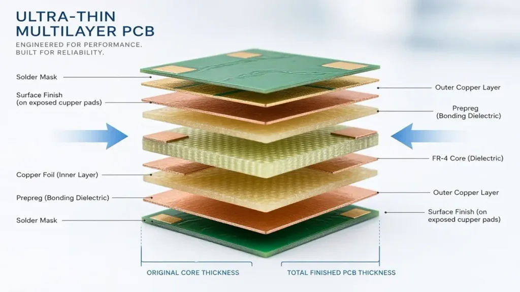
Cross-sectional structure of an ultra-thin core PCB, showing how core dielectric, copper layers, prepreg, solder mask, and surface finish contribute to the finished board thickness.
An ultra-thin core PCB is a printed circuit board built around a thin insulating substrate, typically FR-4, BT resin, or polyimide, to reduce the overall thickness of the finished circuit structure.
The core is an essential structural component. It provides dielectric separation between copper layers, contributes to mechanical rigidity, and influences dimensional stability during lamination and thermal processing.
However, core thickness and finished PCB thickness are two different specifications.
Core thickness describes the nominal thickness of the insulating substrate before the multilayer bonding process.
Finished PCB thickness includes the complete fabricated structure:
- Core dielectric.
- Copper foil on the core surfaces.
- Prepreg bonding layers.
- Additional copper plating.
- Outer-layer solder mask.
- Surface finish.
For example, a 0.1 mm FR-4 core does not produce a 0.1 mm finished PCB automatically. Additional copper, bonding materials, and protective coatings increase the final thickness.
The difference becomes especially important when designing compact electronic products with limited enclosure clearance, low-profile connectors, fine-pitch components, and tightly controlled assembly heights.
At PCBKR, our engineering team evaluates the target finished thickness first, then determines the appropriate combination of core material, core thickness, copper weight, and prepreg construction.
This approach prevents a common procurement mistake: specifying a core thickness without checking whether the complete multilayer structure can satisfy the mechanical envelope.
Core PCB vs. Thin Laminate PCB
| Specification | Core PCB | Finished Thin PCB |
|---|---|---|
| Measurement | Insulating substrate | Complete fabricated board |
| Includes copper | Depends on core specification | Yes |
| Includes prepreg | No | Yes, where applicable |
| Includes plating | No | Yes |
| Includes solder mask | No | Yes, where applicable |
| Main design concern | Dielectric and substrate properties | Overall thickness and dimensional stability |
For an accurate RFQ, buyers should specify both values.
For example:
- Finished thickness: 0.30 mm.
- Core material: High-Tg FR-4.
- Nominal core thickness: 0.10 mm.
- Layer count: 4 layers.
- Copper construction: 0.5 oz base copper.
- Surface finish: ENIG.
This gives the manufacturer enough information to evaluate the complete stackup rather than quote an isolated material thickness.
2. Which Core Thicknesses Are Available for Ultra-Thin PCB Manufacturing?
The appropriate core thickness depends on the number of copper layers, electrical requirements, mechanical loading, and total board thickness target.
PCBKR supports thin-core constructions using FR-4, BT resin, and polyimide materials.
Typical design ranges include:
| Core Material / Parameter | Thickness Range | Typical Application |
|---|---|---|
| FR-4 thin core | 0.075–0.3 mm | Rigid ultra-thin PCBs |
| High-Tg FR-4 | 0.1–0.3 mm | Industrial and automotive electronics |
| BT resin | 0.1–0.2 mm | High-reliability and high-density structures |
| Polyimide substrate | 0.025–0.1 mm | Flexible and rigid-flex circuits |
| Finished ultra-thin PCB | 0.1–0.6 mm | Compact electronic assemblies |
These are material and design capability ranges, not interchangeable finished-board thickness guarantees.
How to Select the Correct Core Thickness
0.075 mm FR-4 Core
This is a specialized thin-core option for applications where dielectric thickness and overall board height are tightly constrained. Handling, dimensional stability, and lamination conditions require particular attention.
0.1 mm FR-4 Core
A practical starting point for compact rigid PCB designs. It can be considered for two-layer and multilayer constructions, depending on the required finished thickness and copper architecture.
0.127–0.152 mm FR-4 Core
These thicknesses provide additional mechanical support while still allowing significant board-height reduction. They are relevant to compact industrial controllers, sensor modules, and multilayer electronics.
0.025–0.1 mm Polyimide
PI is used where flexibility, thin construction, or rigid-flex integration is required. Its mechanical behavior and moisture characteristics differ from glass-reinforced FR-4, so the complete design must be evaluated accordingly.
A supplier should not approve a core thickness based only on the nominal material specification. Panel dimensions, copper distribution, lamination sequence, and final assembly requirements must also be considered.
3. How Do FR-4, BT Resin, and Polyimide Compare for Ultra-Thin PCB Cores?
Core material selection directly affects the reliability of an ultra-thin PCB.
Three material families are particularly relevant: FR-4, BT resin, and polyimide.
Each has different mechanical, thermal, and electrical properties.
High-Tg FR-4 for Rigid Ultra-Thin PCB Structures
High-Tg FR-4 is a practical material choice for rigid ultra-thin PCB applications requiring a balance of manufacturing cost, mechanical strength, and thermal performance.
PCBKR supports FR-4 thin-core construction, including 0.075 mm core options and high-Tg material systems.
Important parameters include:
- Glass transition temperature (Tg).
- Z-axis coefficient of thermal expansion.
- Moisture absorption.
- Copper adhesion.
- Dielectric constant.
- Lamination compatibility.
For multilayer boards exposed to repeated lead-free reflow, high-Tg FR-4 should be evaluated against the assembly temperature profile rather than selected solely by nominal thickness.
BT Resin for High-Density and Thermally Demanding Structures
BT resin is a thermosetting material commonly used in high-density electronic packaging and substrate-related applications.
Its properties can make it suitable for compact multilayer constructions requiring thermal stability and controlled dielectric characteristics.
However, BT resin should not automatically be considered superior to FR-4 for every application.
Material selection should account for:
- Actual Tg and CTE data.
- Moisture absorption.
- Dk and Df at the operating frequency.
- Copper adhesion.
- Lamination and curing requirements.
- Availability of the specified thin-core grade.
BT constructions may require different lamination recipes from conventional FR-4.
Polyimide for Flexible and Rigid-Flex Ultra-Thin Circuits
Polyimide is particularly relevant when the product requires bending, folding, or integration into a compact curved enclosure.
PCBKR supports PI substrate thickness down to 0.025 mm.
Typical applications include wearable electronics, compact sensor assemblies, and flexible interconnect sections.
PI is not simply a thinner replacement for FR-4.
It requires consideration of:
- Flexural requirements.
- Copper type and thickness.
- Adhesive or adhesiveless construction.
- Coverlay thickness.
- Moisture conditioning.
- Stiffener requirements.
- Dynamic or static bending conditions.
Material Selection Matrix
| Engineering Requirement | FR-4 | BT Resin | Polyimide |
|---|---|---|---|
| Rigid PCB construction | Excellent fit | Excellent fit | Application-dependent |
| Flexible circuit construction | Not suitable | Not typical | Preferred |
| Thermal stability | Grade-dependent | Grade-dependent, often high | High |
| Dimensional rigidity | Glass-reinforced structure | Grade-dependent | Lower without reinforcement |
| High-density packaging | Suitable with HDI processes | Suitable | Application-dependent |
| Material cost | Generally economical | Generally higher | Generally higher |
| Main consideration | Tg and CTE | Cure and lamination control | Flexibility and moisture |
The correct selection depends on the actual operating environment and the complete board architecture.
For projects requiring more detailed laminate comparisons, our ultra-thin PCB material selection guide explains the material properties and application trade-offs in greater depth.
4. How Does Core Thickness Affect the Finished PCB Thickness Budget?
Core thickness is only one component of the finished PCB thickness.
For an ultra-thin multilayer board, every dielectric and conductive layer contributes to the final dimensional result.
The basic thickness budget can be expressed as:
Finished PCB Thickness = Total Core Thickness + Total Cured Prepreg Thickness + Total Copper Thickness + Solder Mask Thickness + Surface Finish Thickness
Where:
- Finished PCB Thickness = Total thickness of the fabricated PCB.
- Total Core Thickness = Combined thickness of all insulating core materials.
- Total Cured Prepreg Thickness = Combined thickness of cured bonding dielectric layers.
- Total Copper Thickness = Remaining base copper and plated copper contribution.
- Solder Mask Thickness = Total solder mask thickness on the applicable surfaces.
- Surface Finish Thickness = Thickness contributed by the selected surface finish.
Actual finished thickness must be confirmed from the approved stackup and manufacturing measurements. Copper and resin dimensions change during fabrication, so nominal input thicknesses should not simply be added without considering the process.
Example: A Four-Layer Ultra-Thin Core Construction
Consider a preliminary four-layer rigid PCB structure:
| Stackup Element | Design Specification |
|---|---|
| L1 outer copper | 0.5 oz base copper |
| Dielectric | Prepreg, project-specific cured thickness |
| L2 inner copper | 0.5 oz base copper |
| Core | 0.10 mm FR-4 |
| L3 inner copper | 0.5 oz base copper |
| Dielectric | Prepreg, project-specific cured thickness |
| L4 outer copper | 0.5 oz base copper |
| Protective layers | Solder mask and selected surface finish |
This is a structural example, not a guaranteed 0.3 mm finished-board recipe.
The final thickness depends on the selected prepreg style, resin content, copper plating, solder mask, and surface finish.
Why Thickness Tolerance Becomes More Critical on Thin Cores
A dimensional deviation that appears small on a conventional PCB can become significant on an ultra-thin structure.
For example:
- A 25 μm deviation represents 1.56% of a 1.6 mm board.
- The same 25 μm deviation represents 12.5% of a 0.2 mm board.
This is why the procurement specification should separately identify:
- Nominal core thickness.
- Core material tolerance.
- Nominal finished thickness.
- Finished thickness tolerance.
- Measurement locations.
- Whether solder mask and surface finish are included.
PCBKR evaluates these requirements during stackup and DFM review.
The finished-thickness specification should always be confirmed against the actual construction, rather than inferred from the core designation.
For buyers who need to establish enclosure clearance and board-height requirements, the ultra-thin PCB thickness guide provides a more detailed explanation of finished-board thickness ranges and manufacturing considerations.
5. How Should Copper Weight and Prepreg Be Selected for Thin-Core Stackups?
Copper weight and prepreg selection are closely connected to the mechanical and electrical behavior of ultra-thin PCBs.
A thin core does not automatically support every copper construction.
If copper is too thick relative to the dielectric structure, resin flow, etching, and thickness uniformity become more difficult to control.
Copper Weight Selection
Common copper options include:
- 0.33 oz base copper, approximately 12 μm.
- 0.5 oz base copper, approximately 17.5 μm.
- 1 oz base copper, approximately 35 μm.
The appropriate copper weight depends on current requirements, trace width, layer density, impedance targets, and finished thickness.
For fine-line signal layers, thinner starting copper can help reduce etching compensation and improve trace geometry.
For power layers, heavier copper may be required to satisfy current-carrying and thermal requirements.
The design should balance electrical performance with the total thickness budget.
Prepreg Selection
Prepreg provides the bonding dielectric between copper layers and influences the final spacing of the multilayer construction.
Important parameters include:
- Prepreg style.
- Glass reinforcement.
- Resin content.
- Nominal thickness.
- Cured dielectric thickness.
- Resin flow.
- Compatibility with the core laminate.
Thin-core multilayer designs require particular attention to resin distribution.
Insufficient resin can create weak bonding or local voids. Excessive resin flow can alter dielectric thickness and cause uneven material distribution.
Copper and Prepreg Engineering Considerations
| Design Variable | Potential Risk | Engineering Consideration |
|---|---|---|
| Excessive copper weight | Increased board thickness and etching difficulty | Balance electrical and mechanical requirements |
| Uneven copper distribution | Warpage | Copper balancing and dummy copper |
| Incorrect prepreg style | Resin starvation or excess flow | Match resin content to stackup |
| Asymmetric dielectric layers | Lamination stress | Symmetrical dielectric construction |
| Inconsistent copper geometry | Impedance variation | Controlled trace geometry and validation |
The final copper and prepreg combination should be approved before production tooling.
6. How Is a Symmetrical Multilayer Stackup Designed Around an Ultra-Thin Core?
Multilayer stackup architecture determines whether an ultra-thin PCB can maintain mechanical stability after lamination and assembly.
As the number of layers increases, the manufacturer must manage more than the nominal core thickness.
The complete structure includes:
- Copper layer thickness.
- Core location.
- Prepreg thickness.
- Resin distribution.
- Copper density.
- Dielectric symmetry.
- Via architecture.
Why Symmetrical Stackup Design Matters
During lamination and subsequent thermal processing, different materials expand and contract at different rates.
If the copper distribution or dielectric construction is significantly different on the two sides of the board, internal stress can become unbalanced.
This can cause:
- Board bow and twist.
- Localized deformation.
- Layer registration changes.
- Assembly coplanarity problems.
- Increased stress around vias and component pads.
For this reason, multilayer ultra-thin PCB designs should generally use symmetrical stackup architecture.
Stackup Design Rules
1. Mirror copper distribution
Copper weight and copper coverage should be balanced across corresponding layers whenever the design permits.
2. Balance dielectric construction
Core and prepreg thicknesses should be reviewed around the central plane of the stackup.
3. Review via architecture
Blind, buried, stacked, and staggered microvias should be selected according to layer count, aspect ratio, and reliability requirements.
4. Evaluate panel dimensions
Larger panels are more sensitive to handling deformation and dimensional changes.
5. Consider assembly stress
Board support, component distribution, and reflow conditions should be included in the design review.
PCBKR supports thin-core multilayer configurations, including conventional thin-core constructions and hybrid thin/thick structures. Designs extending to higher layer counts require individual stackup and manufacturing feasibility review.
A symmetrical layer count alone does not guarantee symmetrical mechanical behavior. Copper coverage, resin distribution, and material properties must also be considered.
7. How Does Core Selection Affect Impedance and High-Speed Signal Integrity?
Core selection influences the electrical behavior of a PCB through dielectric thickness, dielectric constant, loss tangent, and the physical relationship between signal traces and reference planes.
These variables become particularly important in compact high-density designs.
Dielectric Thickness and Characteristic Impedance
The distance between a signal layer and its reference plane influences characteristic impedance.
For a microstrip or stripline structure, impedance is affected by:
- Trace width.
- Finished copper thickness.
- Dielectric thickness.
- Dielectric constant.
- Reference-plane geometry.
- Adjacent copper structures.
A thinner dielectric generally changes the required trace geometry for a given impedance target.
Therefore, changing the core or prepreg thickness after routing can invalidate the original impedance calculation.
Core Material and Dielectric Loss
For high-speed or high-frequency designs, the material’s Dk and Df must be evaluated at the relevant frequency.
A standard FR-4 core may be sufficient for many industrial control and embedded applications.
For higher-frequency requirements, a low-loss material may be necessary.
The selection should be based on the actual operating frequency and transmission-line structure rather than the marketing category of the laminate.
PCBKR Signal Integrity Validation
For controlled-impedance projects, PCBKR supports engineering review of:
- Single-ended impedance.
- Differential impedance.
- Signal-to-reference-plane spacing.
- Copper thickness.
- Dielectric construction.
- Impedance coupon design.
- TDR measurement.
Our verification resources include TDR and VNA measurement capability, with VNA equipment supporting measurements up to 70 GHz.
The measurement bandwidth of the instrument should not be confused with the guaranteed operating frequency of every finished PCB. Actual signal performance depends on the complete material system, stackup, trace geometry, connector transitions, and project-specific validation.
For advanced signal-integrity projects, the core design should be coordinated with the broader high-speed PCB architecture from the initial engineering review.
8. Which Lamination Parameters Control Thin-Core Dimensional Stability?
Lamination is one of the most critical manufacturing operations for ultra-thin core PCBs.
Thin dielectric materials are more sensitive to pressure, temperature, resin flow, and mechanical handling than conventional thicker constructions.
A lamination recipe designed for a standard PCB cannot simply be transferred to a thin-core build without engineering review.
Vacuum-Assisted Lamination
PCBKR uses LAUFFER vacuum lamination equipment for multilayer bonding.
Confirmed process capabilities include:
- 80 psi.
- 150 psi.
- 200 psi.
- Vacuum below 50 mbar.
These settings provide process options for different stackup constructions.
The appropriate pressure profile must be determined according to the core material, prepreg resin system, copper distribution, panel dimensions, and curing requirements.
Why Vacuum Matters
Air trapped between dielectric and copper layers can create internal defects.
In thin-core structures, even a small internal void can affect local bonding and become a potential reliability risk during subsequent thermal exposure.
Vacuum-assisted lamination helps remove trapped air before the resin cures.
However, vacuum alone cannot eliminate all lamination defects. Material conditioning, layup quality, resin flow, pressure ramps, and cooling profiles must work together.
Dimensional Stability During Cooling
Different materials have different thermal expansion characteristics.
If cooling is not appropriately controlled, residual stress can develop within the multilayer structure.
For thin-core boards, the manufacturer should review:
- Heating and curing profile.
- Pressure transition points.
- Vacuum conditions.
- Resin flow behavior.
- Cooling rate.
- Panel support.
- Post-lamination thickness distribution.
The broader manufacturing sequence also matters. For a detailed explanation of how imaging, lamination, drilling, plating, and inspection interact, see our ultra-thin PCB manufacturing process guide.
This distinction is important: the Core PCB page explains the engineering role of the substrate, while the manufacturing guide addresses the complete fabrication workflow.
9. How Are LDI Registration and Laser Microvias Controlled on Thin Cores?
Ultra-thin multilayer structures leave less room for manufacturing deviation.
Layer-to-layer registration, trace geometry, and microvia positioning must therefore be evaluated together.
Laser Direct Imaging
PCBKR uses SCREEN Ledia LDI systems for precision imaging.
The verified capability includes:
- 8 μm target imaging capability.
- ±10 μm layer registration control.
LDI removes dependence on conventional phototool stretching and supports fine-line pattern imaging.
However, imaging resolution and layer-to-layer registration are different parameters.
A system’s imaging capability should not be presented as the guaranteed final trace width or finished registration accuracy of every production board.
The actual result depends on:
- Copper surface condition.
- Resist thickness.
- Imaging calibration.
- Etching or plating compensation.
- Panel dimensional changes.
- Lamination registration.
mSAP Fine-Line Fabrication
Modified Semi-Additive Process (mSAP) is important for fine-line structures where conventional subtractive etching becomes increasingly difficult.
The process generally includes:
- Preparing a thin copper seed layer.
- Applying and imaging photoresist.
- Selectively plating copper.
- Removing the photoresist.
- Flash-etching the remaining seed layer.
PCBKR has supported 8/8 μm mSAP capability since Q3 2024.
This capability is relevant to high-density routing and compact multilayer structures where trace geometry must be tightly controlled.
Laser Microvia Processing
PCBKR’s confirmed laser processing capabilities include:
- Mitsubishi UV/CO₂ Laser: 75 μm ±5 μm for microvia processing.
- Picosecond Laser: 50 μm for fine microvia processing.
- SCREEN Ledia LDI: 8 μm target imaging capability.
- mSAP: 8/8 μm fine-line fabrication capability.
Laser selection depends on the material system, dielectric thickness, via diameter, and required hole-wall quality.
For ultra-thin cores, the goal is not simply to produce a smaller via. It is to produce a reliable interconnection without damaging the surrounding dielectric or compromising the copper interface.
Microvia quality should be confirmed through appropriate inspection, including microsection analysis and X-ray where applicable.
10. What Causes Cracking, Delamination, and Warpage in Ultra-Thin Core PCBs?
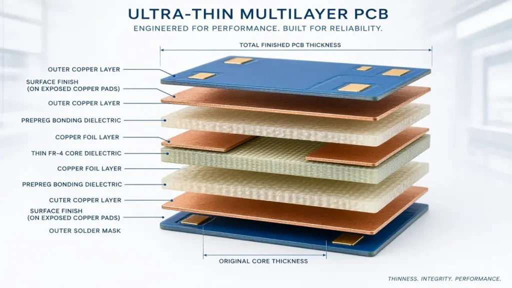
Typical ultra-thin PCB failure modes, including core cracking, resin starvation, interlayer delamination, and excessive board warpage.
Ultra-thin PCBs are particularly sensitive to mechanical and thermal stress because their dielectric structures provide less resistance to deformation.
The most important failure modes should be identified before the design enters production.
Core Cracking
Core cracking may result from:
- Excessive mechanical handling stress.
- Inappropriate drilling conditions.
- Panel bending during transportation.
- Insufficient material support.
- Stress concentration around holes and edges.
Control measures include suitable panel handling, carrier support, appropriate drilling methods, and inspection of the core structure.
Resin Starvation
Resin starvation occurs when insufficient resin remains to form an adequate dielectric bond between layers.
Potential causes include:
- Incorrect prepreg selection.
- Inadequate resin content.
- Excessive resin flow.
- Incorrect lamination pressure.
- Improper material combinations.
The manufacturer should verify the cured dielectric thickness and inspect the bonded interface.
Delamination
Delamination can result from insufficient bonding, moisture, contamination, material incompatibility, or excessive thermal stress.
Control measures include incoming material inspection, controlled lamination, appropriate surface preparation, and cross-sectional verification.
Excessive Warpage
Warpage is particularly important for thin boards undergoing SMT assembly.
Potential causes include:
- Asymmetric copper distribution.
- Uneven dielectric thickness.
- Different material CTE values.
- Unbalanced lamination stress.
- Uneven thermal exposure.
The best preventive approach is to address the mechanical balance during stackup design rather than relying only on final inspection.
Failure Mode and Process Control Matrix
| Failure Mode | Primary Cause | PCBKR Engineering Control | Verification |
|---|---|---|---|
| Core cracking | Handling or drilling stress | Supported panel handling and suitable drilling | Microsection inspection |
| Resin starvation | Incorrect prepreg or resin flow | Prepreg selection and lamination control | Cross-section |
| Delamination | Poor bonding or thermal stress | Material compatibility and vacuum lamination | Microsection and applicable reliability testing |
| Excessive warpage | Asymmetric stackup | Copper balancing and symmetrical construction | Flatness measurement |
| Layer misregistration | Material movement during lamination | LDI and optical alignment | Registration measurement |
| Microvia defects | Laser or plating process variation | Laser parameter and plating control | X-ray and microsection |
| Impedance deviation | Dielectric and copper geometry variation | Stackup review and process control | TDR measurement |
Warpage Control Requires More Than a Flatness Measurement
A board that is flat at room temperature may deform during reflow.
For this reason, OEM buyers should define whether the acceptance requirement applies to:
- As-fabricated flatness.
- Post-reflow flatness.
- Room-temperature bow and twist.
- Temperature-dependent deformation.
A warpage percentage should always be associated with a defined test method, measurement condition, and board configuration.
PCBKR evaluates these requirements according to the application and the agreed acceptance criteria.
Because copper imbalance, material CTE differences, and lamination stress can interact, warpage should be evaluated as a complete structural reliability issue rather than an isolated flatness measurement. For a more detailed discussion of bow, twist, thermal deformation, and practical prevention methods, engineers can refer to our ultra-thin PCB warpage control guide.
11. How Does PCBKR Verify Ultra-Thin Core Quality and Electrical Reliability?
Manufacturing quality must be verified at multiple stages.
For ultra-thin PCB production, final electrical testing alone cannot identify every internal structural problem.
PCBKR uses process inspection, dimensional verification, and electrical testing to evaluate different aspects of board quality.
Incoming Material Inspection
Before production, thin-core materials should be reviewed for:
- Nominal thickness.
- Material grade.
- Copper weight.
- Supplier documentation.
- Lot identification.
- Storage and conditioning requirements.
Material traceability is important because a change in core or prepreg grade can affect the entire stackup.
In-Process Inspection
Relevant manufacturing checks include:
- Inner-layer AOI.
- LDI imaging verification.
- Layer registration measurement.
- Post-lamination thickness measurement.
- Microvia inspection.
- Copper plating inspection.
3D AOI and X-ray inspection provide complementary information.
AOI evaluates accessible optical features, while X-ray is used for internal structural inspection.
Electrical Verification
Electrical verification depends on the design requirements.
PCBKR supports:
- Flying probe electrical testing.
- Four-wire Kelvin resistance measurement.
- TDR impedance validation.
- VNA measurement up to 70 GHz.
For controlled-impedance boards, test coupons should represent the relevant dielectric and copper construction.
A TDR report should identify the test structure, target impedance, measured values, and acceptance limits.
First Article Inspection Documentation
For OEM projects, the first-article package should include the applicable records:
- Approved stackup drawing.
- Material specifications.
- Core and finished-thickness measurements.
- Cross-sectional photographs.
- Copper thickness measurements.
- Registration inspection results.
- Electrical test report.
- TDR report, when impedance control is required.
- X-ray inspection results, when applicable.
- Agreed reliability test results.
This documentation gives the buyer a basis for approving the manufacturing process before committing to repeat orders.
12. What Should OEM Buyers Include in an Ultra-Thin Core PCB RFQ?
An incomplete RFQ creates unnecessary quotation delays and can lead to incorrect material assumptions.
For an ultra-thin core PCB, the buyer should provide the complete mechanical and electrical requirements rather than simply requesting the thinnest available substrate.
Ultra-Thin Core PCB RFQ Checklist
| RFQ Item | Required Information | Why It Matters |
|---|---|---|
| Finished thickness | Nominal thickness and tolerance | Defines the complete dimensional target |
| Core material | FR-4, BT, PI or specified grade | Determines material properties |
| Core thickness | Nominal thickness and tolerance | Defines dielectric construction |
| Layer count | 2, 4, 6 or higher | Determines stackup complexity |
| Copper weight | Base and finished copper thickness | Affects current capacity and thickness |
| Prepreg | Material style and dielectric requirement | Controls bonding and dielectric spacing |
| Trace/space | Minimum line and spacing | Determines imaging and etching process |
| Via structure | Through, blind, buried, stacked or staggered | Determines drilling and reliability requirements |
| Impedance | Single-ended and differential targets | Defines electrical design requirements |
| Surface finish | ENIG, OSP, ENEPIG or other | Affects assembly and surface requirements |
| Panel dimensions | Board and panel size | Affects handling and dimensional stability |
| Quantity | Prototype, NPI and production volumes | Supports process and quotation planning |
| Inspection | AOI, X-ray, microsection, TDR | Defines acceptance documentation |
What Buyers Should Request From the Manufacturer
Beyond the initial quotation, procurement teams should request evidence that the supplier can manufacture the specified structure.
Recommended documents include:
- Material datasheets and certificates.
- Approved stackup proposal.
- Lamination process capability.
- Core thickness measurement records.
- Cross-sectional micrographs.
- Registration inspection results.
- Impedance coupon measurements.
- Applicable reliability reports.
Important Information for RFQ Submission
Please send the following to PCBKR:
- Gerber or ODB++ files.
- Drill files.
- Stackup drawing.
- Target finished thickness.
- Core material preference.
- Copper weight.
- Surface finish.
- Quantity and delivery requirements.
- Special mechanical or electrical acceptance criteria.
Our engineering team can then review material compatibility, stackup feasibility, and manufacturing risks before quotation.
13. How Can You Qualify an Ultra-Thin Core PCB Manufacturer for Repeat Production?
A supplier that can produce one thin PCB prototype is not necessarily qualified for repeat production.
OEM buyers should evaluate whether the manufacturer can maintain the same material, dimensional, and electrical characteristics across different production lots.
Supplier Qualification Checklist
1. Verify Actual Thin-Core Manufacturing Experience
Ask for examples of multilayer boards using comparable core thicknesses, materials, and panel dimensions.
A supplier should be able to explain how the construction was manufactured rather than simply showing a finished PCB photograph.
2. Review Equipment and Process Capability
Confirm that the factory has suitable:
- LDI imaging equipment.
- Vacuum lamination systems.
- Laser drilling equipment.
- Fine-line processing capability.
- AOI and X-ray inspection.
- Electrical testing facilities.
Equipment specifications should be supported by process records and inspection evidence.
3. Review First-Article Inspection Results
Check whether the supplier can provide dimensional measurements, microsection reports, and electrical verification data.
The inspection package should correspond to the actual production stackup.
4. Evaluate Material and Lot Traceability
Confirm that the core material, prepreg, copper foil, and surface finish can be traced to their relevant supplier lots.
This becomes particularly important when the project depends on a specific BT or high-Tg FR-4 material grade.
5. Confirm Repeat-Production Controls
Ask how the supplier monitors:
- Core thickness variation.
- Finished-board thickness.
- Layer registration.
- Copper distribution.
- Warpage.
- Electrical performance.
- Process changes between lots.
A qualified manufacturer should be able to explain how deviations are identified and how corrective actions are documented.
Why PCBKR for Ultra-Thin Core PCB Manufacturing?
Shenzhen Hongda Circuit Technology Co., Ltd. supports OEM projects requiring thin-core rigid PCB, multilayer PCB, and flexible or rigid-flex constructions.
Our engineering and manufacturing resources include:
- FR-4 thin cores from 0.075 mm.
- Polyimide substrates down to 0.025 mm.
- Multilayer and hybrid stackup construction.
- SCREEN Ledia LDI imaging.
- LAUFFER vacuum lamination.
- Mitsubishi UV/CO₂ laser processing.
- Picosecond laser processing.
- 8/8 μm mSAP capability.
- AOI, X-ray, TDR, and electrical inspection.
These capabilities support different levels of ultra-thin PCB complexity. Final manufacturability depends on the complete stackup, material selection, board dimensions, and required acceptance criteria.
For OEM programs, our objective is to establish a manufacturing specification that can be reviewed, verified, and repeated rather than relying on an isolated prototype result.
Procurement FAQ: Ultra-Thin Core PCB
What Is the Difference Between PCB Core Thickness and Finished Board Thickness?
Core thickness refers to the insulating substrate before multilayer bonding. Finished PCB thickness includes the core, copper, prepreg, plating, solder mask, and surface finish where applicable. Both values should be specified separately in an RFQ.
What Is the Minimum FR-4 Core Thickness for Multilayer PCB Manufacturing?
PCBKR supports FR-4 thin-core options starting at 0.075 mm. However, the minimum practical thickness for a specific multilayer project depends on layer count, copper weight, panel dimensions, prepreg construction, and manufacturing requirements.
Is BT Resin Better Than FR-4 for Ultra-Thin Multilayer PCBs?
Not necessarily. BT resin can offer advantages for certain high-density and thermally demanding applications, while high-Tg FR-4 is often a more economical choice for rigid PCB designs. The decision should be based on Tg, CTE, Dk/Df, moisture absorption, and assembly conditions.
How Can Manufacturers Prevent Warpage and Delamination in Thin-Core PCBs?
The main controls include symmetrical stackup design, balanced copper distribution, suitable prepreg selection, vacuum-assisted lamination, controlled pressure and temperature profiles, and cross-sectional inspection. Warpage should also be evaluated under the relevant assembly conditions.
What Information Should OEM Buyers Provide When Requesting an Ultra-Thin Core PCB Quotation?
Provide the Gerber or ODB++ files, layer count, core material, nominal core thickness, target finished thickness and tolerance, copper weight, prepreg requirements, via structure, surface finish, impedance requirements, board dimensions, and production quantity. Complete information helps the manufacturer evaluate the stackup and quotation accurately.
Ready to Source Your Ultra-Thin Core PCB?
Shenzhen Hongda Circuit Technology Co., Ltd. provides ultra-thin core PCB manufacturing and engineering support for OEMs developing compact, high-density electronic products.
Whether your design requires a 0.075 mm FR-4 core, a 0.025 mm polyimide substrate, a thin-core multilayer stackup, or an advanced fine-line mSAP construction, our engineering team can review the material selection, thickness budget, lamination architecture, and inspection requirements.
Send your PCB design files and target specifications for an engineering feasibility revie
Contact PCBKR
- Company: Shenzhen Hongda Circuit Technology Co., Ltd.
- Website: https://www.pcbkr.com/
- Email: sales@pcbkr.com
- Manufacturing: Baoan, Shenzhen, China
Request an Ultra-Thin Core PCB quotation and engineering review.
About the Author
David Chen LinkedIn Profile
David Chen is a Senior RF/PCB Process Engineer at Shenzhen Hongda Circuit Technology Co., Ltd., with over 12 years of experience in high-frequency PCB fabrication, impedance-controlled stack-up design, and Rogers/PTFE laminate processing. He also boasts an extensive professional background in PCBA manufacturing, PCBA testing, and PCBA optimization, with specialized expertise in high-precision PCBA fault analysis and rigorous PCBA reliability testing. The author has worked with high-layer-count server PCB fabrication, ultra-low-loss backplane stackups, and thermo-mechanical reliability optimization for AI infrastructure projects involving 112G and 224G PAM4 architectures. Skilled in complex circuit design and cutting-edge advanced PCB manufacturing processes, he delivers solutions that elevate product durability and performance across industrial applications. His technical articles focusing on PCBA manufacturing workflows and testing methodologies are widely cited by industry peers and technical platforms, and have gained attention and recognition from industry colleagues.