Custom PCIe Signal Expansion Board PCB Manufacturing for OEM Projects
A Custom PCIe Signal Expansion Board extends or routes PCI Express connectivity between a host system and connected devices. Its design depends on PCIe generation, lane configuration, connector selection, signal-integrity requirements, power delivery, and mechanical constraints. Shenzhen Hongda Circuit Technology Co., Ltd. provides custom multilayer PCB fabrication and optional PCBA assembly for OEM projects.
What Is a Custom PCIe Signal Expansion Board and Where Is It Used?
A Custom PCIe Signal Expansion Board is a purpose-built printed circuit board designed to extend, route, or distribute PCI Express connectivity between a host platform and one or more downstream devices.
Unlike a standard off-the-shelf expansion card, a custom board can be designed around specific connector positions, lane configurations, board dimensions, device interfaces, and system integration requirements.
OEM projects may require different board architectures depending on the application.
Common Applications of Custom PCIe Expansion Boards
| Application | Typical Expansion Requirements |
|---|---|
| Server and storage systems | NVMe SSD connectivity, storage expansion, and device interconnection |
| Industrial computers | Custom PCIe interfaces for embedded controllers and industrial modules |
| Networking equipment | PCIe-connected network interface modules and I/O expansion |
| AI and computing systems | GPU, FPGA, and accelerator connectivity |
| Test and measurement equipment | Custom PCIe signal routing and interface boards |
| Embedded computing | Host-to-device connectivity within limited mechanical space |
Expansion Cards, Riser Cards, and Backplanes: What Is the Difference?
These product categories are related but serve different mechanical and electrical purposes.
- PCIe expansion card: A board that connects to a host PCIe slot and provides additional device interfaces or functions.
- PCIe riser card: A board or assembly that changes the physical position or orientation of a PCIe connection, often to accommodate chassis constraints.
- PCIe adapter board: A board that converts or routes between different connector formats or interface arrangements.
- PCIe backplane: A larger interconnection structure designed to connect multiple boards, modules, or devices.
PCBKR focuses on manufacturing custom PCB structures according to customer-approved designs and specifications. Whether a project requires a passive adapter, a riser, a switch-based expansion board, or a more complex interconnection PCB, the manufacturing requirements should be reviewed individually.
Which PCIe Expansion Architectures, Connectors, and Lane Configurations Can Be Customized?
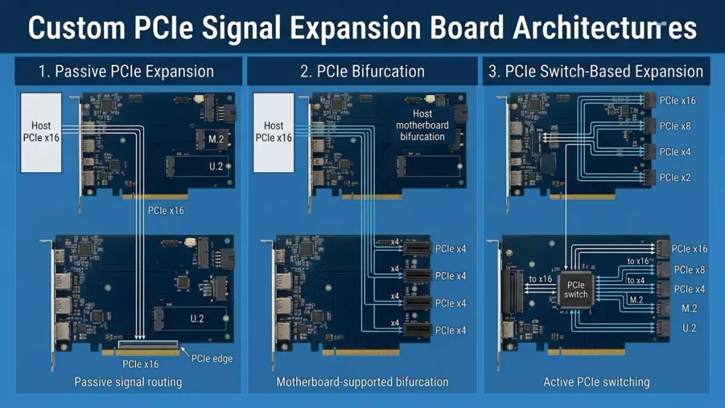
Custom PCIe Signal Expansion Board Architectures and Lane Configurations
The architecture determines how PCIe signals travel from the host system to downstream devices. It also affects the required components, PCB routing, connector arrangement, power distribution, and system compatibility.
Before requesting a quotation, OEM buyers should identify whether their project requires passive signal routing, host-supported lane bifurcation, or an active PCIe switching architecture.
1. Passive PCIe Expansion
A passive PCIe expansion board routes existing PCIe signals between a host connector and downstream device connectors.
It does not independently create additional PCIe lanes or increase the host system’s available PCIe bandwidth.
A passive design may be suitable when the host platform supports the required lane configuration and the complete signal channel meets the applicable electrical requirements.
2. PCIe Bifurcation-Based Expansion
PCIe bifurcation divides the available lanes of a host PCIe connection into smaller lane groups.
For example, a supported x16 host connection may be configured as:
- x8 + x8
- x4 + x4 + x4 + x4
However, the actual configuration depends on CPU, motherboard, chipset, BIOS, and platform support.
A passive expansion board cannot enable bifurcation if the host platform does not support it.
For OEM projects, buyers should provide the motherboard model, CPU platform, intended lane configuration, and downstream device count during the engineering review.
3. PCIe Switch-Based Expansion
A PCIe switch allows a host connection to communicate with multiple downstream PCIe devices through a switching topology.
Unlike passive lane routing, a switch-based design includes active components and requires additional engineering considerations.
| Design Parameter | Information Required |
|---|---|
| PCIe switch | Manufacturer and exact device model |
| Upstream port | Host-side lane configuration |
| Downstream ports | Number of devices and port allocation |
| Lane configuration | Available lanes per downstream device |
| Clock architecture | Reference clock and clock distribution requirements |
| Power | Switch and downstream device power requirements |
| Thermal design | Device power dissipation and cooling arrangement |
A PCIe switch does not automatically guarantee compatibility with every motherboard or operating system. Platform support, firmware configuration, device enumeration, and system validation remain important.
4. Retimer and Redriver Applications
Retimers and redrivers are different types of signal-conditioning components.
A redriver amplifies or equalizes an incoming signal without performing the same clock recovery and retransmission function as a retimer.
A retimer performs clock and data recovery and retransmits the signal, helping address certain channel-loss and signal-integrity challenges.
Whether either device is required depends on the complete channel design, component specifications, and system requirements.
Common PCIe Connectors and Interfaces
Custom expansion boards may use different connectors depending on the target platform and device.
| Interface | Typical Application |
|---|---|
| PCIe edge connector | Host motherboard connection |
| M.2 | Compact storage and embedded device interfaces |
| U.2 / U.3 | Enterprise storage connectivity |
| MCIO | High-density internal cable connections |
| SlimSAS | Storage and high-speed internal connectivity |
| Board-to-board connector | Compact embedded and modular systems |
| Custom cable connector | OEM-specific interconnection requirements |
Connector selection must account for electrical compatibility, pin assignment, mechanical dimensions, signal performance, and component availability.
For M.2 projects, buyers should also distinguish between SATA and PCIe/NVMe interfaces. Similar connector appearances do not mean that the electrical protocols are interchangeable.
PCIe Lane Configuration and Host Compatibility
The connector’s physical size does not necessarily indicate the number of electrically available lanes.
A card with an x16 edge connector may operate with fewer lanes depending on the host slot and the board design.
For example, a project requiring four downstream x4 devices needs a suitable lane allocation or switching architecture. The actual implementation must be confirmed against the host platform.
PCBKR recommends including a lane map or connection block diagram in the RFQ package whenever the project involves multiple devices.
How Should PCB Stackup and Material Be Selected for a Custom PCIe Expansion Board?
PCB stackup selection affects impedance, insertion loss, crosstalk, power distribution, mechanical stability, and manufacturing feasibility.
A suitable stackup cannot be selected from PCIe generation alone. The design must consider the complete electrical channel, including PCB traces, vias, connectors, cables, and device interfaces.
Key PCB Stackup Considerations
| Stackup Parameter | Engineering Consideration |
|---|---|
| Layer count | Available routing layers and signal-layer allocation |
| Dielectric thickness | Controlled-impedance design and field distribution |
| Dk | Dielectric constant and propagation characteristics |
| Df | Dielectric loss characteristics |
| Copper thickness | Impedance, conductor loss, and current capacity |
| Reference planes | Continuous return paths for high-speed signals |
| Board thickness | Connector and mechanical compatibility |
| Copper distribution | Lamination balance and manufacturing stability |
How Should Low-Loss Materials Be Selected?
Material selection should be based on the required channel performance, not simply on the highest available material specification.
For a high-speed PCIe board, engineering review may consider:
- Dielectric loss characteristics.
- Dielectric constant consistency.
- Copper roughness.
- Frequency-dependent electrical performance.
- Lamination compatibility.
- Thermal and mechanical requirements.
- Material availability and production cost.
Low-loss materials may be appropriate when the channel budget is tight, but not every PCIe expansion board requires an advanced high-frequency laminate.
The material and stackup should be agreed upon before production.
For additional material and high-frequency PCB information, see High Frequency PCB.
Why Are Continuous Ground Reference Planes Important?
High-speed differential routing requires suitable reference structures and return-current paths.
Ground-plane interruptions, poorly designed transitions, and unnecessary routing detours can increase signal-integrity risk.
A stackup review should therefore examine the relationship between signal layers, ground planes, power planes, and connector breakout areas.
How Do Impedance, Signal Routing, and Channel Loss Affect PCIe Performance?
PCIe signal integrity depends on the electrical behavior of the complete transmission channel.
Even when the PCB passes basic continuity and isolation tests, an unsuitable impedance profile, excessive insertion loss, connector discontinuities, or poor routing may affect high-speed link performance.
Controlled Differential Impedance
PCIe high-speed signals use differential transmission.
The required differential impedance must be defined according to the applicable PCIe implementation, device documentation, connector specifications, and system design requirements.
It should not be assumed that one impedance value applies to every PCIe project.
The PCB manufacturer needs the approved stackup and impedance requirements to calculate appropriate trace width, spacing, dielectric thickness, and copper geometry.
Differential Pair Routing Requirements
Important routing considerations include:
- TX and RX differential pair separation.
- Intra-pair length matching.
- Appropriate pair-to-pair spacing.
- Continuous reference planes.
- Controlled layer transitions.
- Connector breakout geometry.
- Avoidance of unnecessary stubs and discontinuities.
Understanding PCIe Channel Loss
A PCIe channel may contain several elements:
- Host transmitter and package.
- Host-side PCB routing.
- PCB vias and layer transitions.
- Connectors and cable assemblies, if present.
- Expansion board routing.
- Downstream connector and device package.
- Receiver input.
Each element contributes to the overall channel behavior.
| Signal Integrity Parameter | Why It Matters |
|---|---|
| Differential impedance | Reduces impedance discontinuities |
| Insertion loss | Indicates signal attenuation through the channel |
| Return loss | Indicates signal reflections |
| Crosstalk | Evaluates unwanted coupling between signal paths |
| Intra-pair skew | Helps maintain differential signal timing |
| S-parameters | Characterize channel frequency-domain behavior |
For demanding projects, the OEM design team may provide channel simulation results, S-parameter requirements, or an approved routing specification.
PCBKR can review manufacturing requirements against the supplied design documentation. Any additional signal-integrity testing should be defined in the RFQ, including test method, frequency range, fixture, and acceptance criteria.
How Do PCB Vias, Backdrilling, and HDI Processes Affect PCIe Signal Integrity?
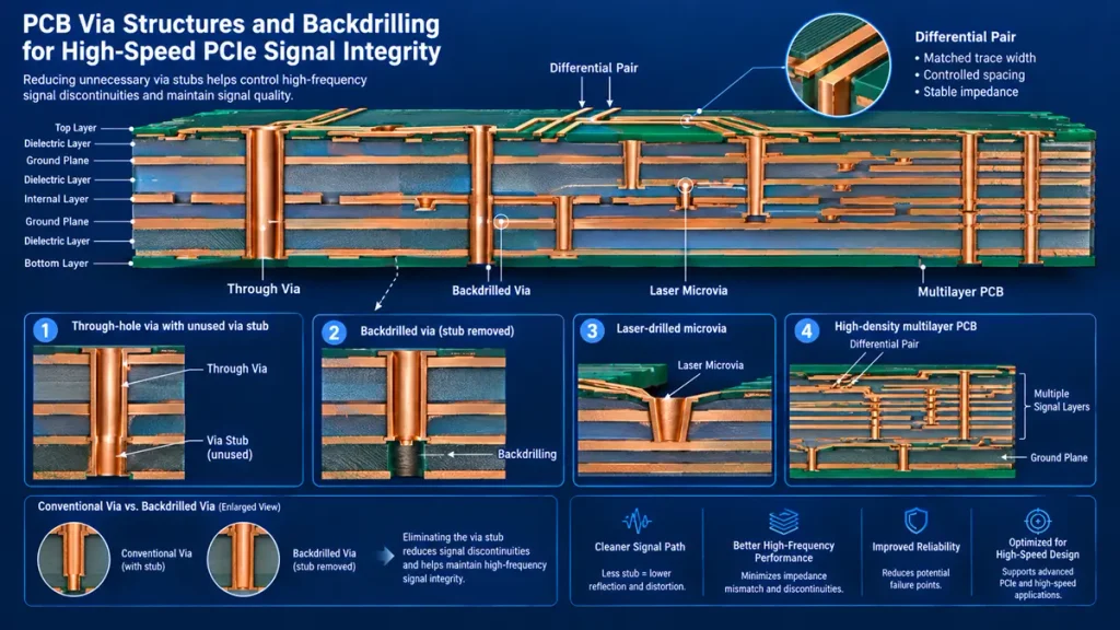
PCIe PCB Via Structures, Backdrilling, and HDI Manufacturing
Vias connect PCB signal layers, but their geometry can affect high-speed transmission.
A poorly controlled via transition may introduce impedance discontinuities and unwanted parasitic effects.
For PCIe expansion boards with multiple signal layers or dense connector areas, via design and manufacturing capability should be considered during the initial engineering review.
Via Structures for High-Speed PCB Designs
| Via Type | Typical Use |
|---|---|
| Through-hole via | General layer-to-layer connection |
| Blind via | Connects an outer layer to selected inner layers |
| Buried via | Connects internal layers |
| Laser microvia | Supports high-density interconnection |
| Backdrilled via | Removes unwanted via stub length where required |
Why Does Via Stub Length Matter?
A through-hole via may contain an unused conductive section beyond the signal connection point.
This unused section is called a via stub.
At higher frequencies, via stubs can introduce resonance and degrade signal transmission.
Backdrilling can remove part of the unused stub to reduce its electrical impact.
However, backdrilling is not automatically required for every PCIe board. The need depends on signal frequency, via geometry, stackup, channel budget, and design requirements.
How Does HDI Manufacturing Support Dense PCIe Expansion Boards?
High-density connector layouts and compact expansion boards may require smaller vias, finer traces, and more complex multilayer structures.
PCBKR’s manufacturing capabilities include:
| Manufacturing Process | PCBKR Capability | Potential Engineering Application |
|---|---|---|
| SCREEN LDI | 8 µm target / ±10 µm | Fine-line imaging and pattern transfer |
| Mitsubishi UV/CO₂ laser | 75 µm ±5 µm | Laser microvia processing |
| Picosecond laser | 50 µm | Fine laser processing requirements |
| mSAP | 8/8 µm capability since Q3 2024 | High-density fine-line circuit fabrication |
| LAUFFER vacuum lamination | 80 / 150 / 200 psi; vacuum below 50 mbar | Multilayer vacuum lamination process control |
These figures describe manufacturing process capabilities. They should not be interpreted as guaranteed finished-board tolerances for every PCIe project.
Actual manufacturability depends on the approved design, material system, layer count, board thickness, via structure, and process requirements.
For additional information, see:
How Should Power Delivery, Thermal Management, and Mechanical Fit Be Designed?
A PCIe expansion board must satisfy more than signal-routing requirements.
Power delivery, thermal behavior, connector loading, and mechanical integration can determine whether a board is suitable for the target system.
Power Distribution Requirements
The power design should be reviewed according to the host interface and connected devices.
Important RFQ information includes:
- Required input voltage.
- Power rails and voltage tolerance.
- Maximum current per power rail.
- Connector current requirements.
- Copper thickness and power trace dimensions.
- Decoupling capacitor requirements.
- Power-plane allocation.
- Protection and monitoring requirements, where applicable.
A board containing active components such as PCIe switches or signal-conditioning devices may require additional power-distribution planning.
Thermal Management for Active Expansion Boards
Thermal considerations become particularly important when the board contains PCIe switches, high-power controllers, or multiple storage devices.
The design review should consider:
- Component power dissipation.
- Heat-source distribution.
- Heatsink dimensions and mounting.
- Forced-air or natural-convection cooling.
- Chassis airflow.
- Component height restrictions.
- Temperature limits specified by component manufacturers.
A thermal requirement should be provided as a measurable target, such as an operating-temperature range or permitted component temperature under defined test conditions.
Mechanical Integration and Connector Placement
Mechanical compatibility should be confirmed before PCB fabrication.
| Mechanical Parameter | Required Information |
|---|---|
| Board dimensions | Length and width |
| Board thickness | Nominal thickness and tolerance |
| Form factor | Full-height, low-profile, or custom |
| Mounting holes | Position, diameter, and tolerance |
| Edge connector | Contact dimensions and insertion requirements |
| Component clearance | Maximum component height |
| Chassis restrictions | Available space and airflow |
| Cable interface | Connector location and cable routing constraints |
OEM buyers should provide a mechanical drawing, preferably in DXF or another agreed engineering format, along with the connector manufacturer’s part numbers.
A mechanically compatible PCB design should be checked against the actual host board, chassis, and connected devices.
Which PCB Fabrication, Inspection, and Electrical Testing Processes Are Required?
Manufacturing quality depends on process control, inspection planning, and clearly defined acceptance criteria.
For a custom PCIe expansion board, the required inspection and testing scope should be established before quotation.
PCB Fabrication and DFM Review
Before production, the manufacturing review should examine:
- Gerber or ODB++ data.
- Approved stackup.
- Minimum line width and spacing.
- Drill and via structures.
- Board thickness.
- Copper distribution.
- Impedance requirements.
- Mechanical tolerances.
- Surface finish.
- Manufacturing notes and acceptance criteria.
The purpose of DFM review is to identify potential manufacturing risks before they affect production.
Inspection and Electrical Testing
PCBKR has inspection and testing capabilities that may be applied according to the board structure and customer requirements.
| Inspection or Test | Purpose |
|---|---|
| 3D AOI | Inspection of applicable surface features |
| X-ray inspection | Internal inspection of applicable structures and assembled joints |
| Flying probe testing | Electrical continuity and isolation checks |
| 4-wire Kelvin measurement | Low-resistance measurement where required |
| Controlled-impedance testing | Verification against agreed impedance requirements |
| TDR / VNA testing | High-frequency electrical characterization when specified |
PCBKR has VNA equipment with capability up to 70 GHz. Actual project testing depends on the required frequency range, calibration, fixture, test coupon, and agreed acceptance method.
PCB Testing Is Not the Same as PCIe System Validation
This distinction is important for OEM procurement.
A PCB can pass fabrication inspection and electrical continuity testing without proving that the complete PCIe system will operate correctly.
| Validation Item | Typical Scope |
|---|---|
| PCB fabrication inspection | Board dimensions, visual quality, and manufacturing features |
| Continuity and isolation | Electrical connection checks |
| Impedance testing | Verification against specified impedance requirements |
| TDR / VNA / S-parameters | High-frequency channel characterization |
| PCIe link training | System-level link initialization |
| Device enumeration | Host and operating-system recognition |
| BIOS compatibility | Platform configuration and firmware support |
| Protocol compliance | Compliance testing using suitable test equipment and procedures |
| Thermal validation | Testing in the specified operating environment |
The OEM or system design team should define who is responsible for system-level validation.
If PCIe link training, protocol compliance, or motherboard compatibility testing is required, the RFQ should explicitly identify the test scope, equipment, fixtures, and acceptance criteria.
How Can OEM Buyers Evaluate a Custom PCIe Signal Expansion Board Manufacturer?
Selecting a supplier for a custom PCIe board requires more than comparing PCB prices.
The manufacturer should be able to review the fabrication requirements, identify production risks, and provide evidence of relevant manufacturing and inspection capabilities.
1. Review High-Speed PCB Manufacturing Capability
Ask the supplier about:
- Multilayer PCB fabrication.
- Controlled-impedance manufacturing.
- Fine-line circuit processing.
- Laser microvia capability.
- Backdrilling, where required.
- Material and stackup handling.
- Board thickness and registration control.
The capability should match the actual design rather than relying on general statements about advanced PCB manufacturing.
2. Check Inspection and Process Control
Buyers should request details about:
- AOI and X-ray inspection.
- Electrical testing.
- Impedance testing.
- Process documentation.
- Lot traceability.
- Nonconformance handling.
- Inspection reports and acceptance criteria.
Where process capability values are provided, buyers should clarify which process, measurement method, and production population they represent.
3. Evaluate Prototype and Production Support
A suitable supplier should be able to discuss the manufacturing requirements for different project stages:
| Project Stage | Main Procurement Consideration |
|---|---|
| Prototype | Engineering review and initial fabrication |
| Pilot production | Process repeatability and inspection |
| Small batch | Production scheduling and quality consistency |
| Mass production | Process control, traceability, and delivery planning |
4. Confirm PCB and PCBA Service Scope
Some OEM projects require PCB fabrication only, while others require component sourcing and assembly.
If PCBA is needed, buyers should clarify whether the supplier can support:
- SMT assembly.
- Through-hole assembly.
- Component sourcing according to the approved BOM.
- AOI and X-ray inspection where applicable.
- Functional or electrical testing according to an agreed test plan.
5. Evaluate the Engineering Review Process
Before placing an order, buyers should confirm that the supplier understands the project requirements.
A practical workflow is:
RFQ Review → DFM Review → Stackup and Manufacturing Confirmation → PCB Fabrication → Inspection and Electrical Testing → Optional PCBA → Shipment
For a custom PCIe project, the most important point is that the manufacturer and OEM agree on the approved files, manufacturing specifications, and test responsibilities before production begins.
What Files and Technical Specifications Should You Include in a PCIe Expansion Board RFQ?
A complete RFQ helps the manufacturer evaluate technical feasibility, identify missing information, and prepare a more accurate quotation.
OEM buyers do not need to have every design parameter finalized before contacting PCBKR. Unknown values can be marked as TBD, provided the available project information is sufficient for an initial review.
1. Product and Architecture Information
| RFQ Item | Information to Provide |
|---|---|
| Product name | Custom PCIe Signal Expansion Board |
| Application | Server, storage, networking, industrial, computing, or other |
| Board function | Passive routing, active expansion, or signal conditioning |
| PCIe generation | Gen 3, Gen 4, Gen 5, Gen 6, or project-specific |
| Lane configuration | x1, x2, x4, x8, or x16 |
| Expansion topology | One-to-one, one-to-multiple, or switch-based |
| Target devices | NVMe SSD, FPGA, GPU, NIC, or other |
| Block diagram | Host-to-device connection diagram |
2. Connector and Mechanical Specifications
| RFQ Item | Information to Provide |
|---|---|
| Host connector | PCIe edge connector, cable, or board-to-board |
| Device connector | M.2, U.2, U.3, MCIO, SlimSAS, or custom |
| Connector part number | Manufacturer and exact part number |
| Board dimensions | Length, width, and thickness |
| Mechanical drawing | DXF or approved mechanical file |
| Mounting | Hole positions and dimensions |
| Form factor | Full-height, low-profile, or custom |
| Clearance | Component height and chassis restrictions |
3. Electrical and Signal-Integrity Specifications
| RFQ Item | Information to Provide |
|---|---|
| Differential impedance | Target value and tolerance |
| Insertion loss | Channel loss requirements, if defined |
| Return loss | Required limits, if defined |
| Pair skew | Intra-pair and inter-pair requirements |
| Lane mapping | TX/RX and lane assignments |
| Reference clock | Clock frequency and distribution requirements |
| Routing constraints | Critical trace lengths and topology |
| Via structure | Through, blind, buried, or backdrilled |
| SI documentation | Simulation data or S-parameters, if available |
4. PCB Manufacturing Specifications
| RFQ Item | Information to Provide |
|---|---|
| Layer count | Total number of layers |
| Stackup | Approved stackup or target structure |
| Material | Specified laminate or electrical requirements |
| Copper weight | Inner and outer copper thickness |
| Minimum line/space | Required trace width and spacing |
| Minimum drill | Mechanical and laser drill requirements |
| Board thickness | Finished thickness and tolerance |
| Surface finish | ENIG, HASL, Immersion Silver, OSP, or other |
| Solder mask | Color and special requirements |
| Impedance coupon | Required coupon structure and test criteria |
5. Power and Thermal Requirements
| RFQ Item | Information to Provide |
|---|---|
| Input power | Input voltage and source |
| Power rails | Required voltage rails |
| Maximum current | Maximum current per rail |
| Power consumption | Expected board-level power |
| Thermal limits | Operating temperature and permitted temperature rise |
| Cooling method | Natural convection, forced air, or heatsink |
| High-current areas | Specified copper thickness and routing requirements |
6. PCBA and Testing Requirements
| RFQ Item | Information to Provide |
|---|---|
| Assembly scope | PCB only or PCB plus PCBA |
| BOM | Approved component list |
| Pick-and-place | Centroid or XY data |
| Assembly drawing | Component placement and assembly details |
| Programming | Firmware or configuration requirements, if applicable |
| Inspection | AOI, X-ray, or other requirements |
| Electrical testing | Continuity, isolation, and impedance |
| SI validation | TDR, VNA, S-parameters, or other specified tests |
| Acceptance criteria | Required test procedures and pass/fail limits |
7. Commercial and Production Requirements
| RFQ Item | Information to Provide |
|---|---|
| Prototype quantity | Initial sample quantity |
| Pilot quantity | Planned pilot batch |
| Production quantity | Estimated mass-production quantity |
| Annual demand | Forecast annual volume |
| Target lead time | Required delivery schedule |
| Delivery destination | Country or region |
| Packaging | ESD protection and packaging requirements |
| Quality documents | Inspection reports and traceability requirements |
| Target cost | Optional target budget |
Recommended Files for an Initial RFQ
For a more efficient engineering and quotation review, prepare the following files where available:
- Gerber or ODB++ fabrication data.
- PCB stackup and impedance requirements.
- Bill of Materials (BOM), if PCBA is required.
- Pick-and-place files.
- Mechanical drawings.
- Connector datasheets and part numbers.
- Lane mapping or architecture block diagram.
- SI simulation results or channel requirements, if available.
- Testing and acceptance specifications.
Not all files must be finalized before the first discussion. If your project is still at the concept stage, you can start with a block diagram, target PCIe generation, lane configuration, connector requirements, mechanical constraints, and estimated quantity.
Request a Custom PCIe Expansion Board Manufacturing Quote
Shenzhen Hongda Circuit Technology Co., Ltd. supports custom PCB manufacturing and optional PCBA assembly for OEM electronic projects.
If you are developing a custom PCIe signal expansion board, send your available design files and technical requirements for an initial manufacturing review.
Project information to include:
- PCIe generation and lane configuration.
- Passive or switch-based expansion architecture.
- Connector types and target devices.
- PCB dimensions and layer count.
- Stackup and impedance requirements.
- Prototype and production quantities.
- PCB-only or PCB plus PCBA requirements.
Contact PCBKR
Shenzhen Hongda Circuit Technology Co., Ltd.
Email: sales@pcbkr.com
Website: https://www.pcbkr.com/
Submit your design files and project requirements to discuss PCB fabrication, optional assembly, manufacturing feasibility, and quotation.
What Should Buyers Know Before Ordering a Custom PCIe Signal Expansion Board?
Can PCBKR manufacture custom PCIe expansion boards for different PCIe generations?
PCBKR can review custom multilayer PCB manufacturing requirements for projects specifying different PCIe generations. Manufacturing feasibility depends on the approved design, material, stackup, impedance requirements, connector selection, and production specifications. PCIe system performance must be validated according to the project’s agreed test plan.
Can PCBKR manufacture passive and PCIe switch-based expansion boards?
PCBKR can review PCB fabrication requirements for both passive and active expansion-board designs. For switch-based projects, buyers should provide the approved switch device, port configuration, schematic, layout files, BOM, and assembly requirements. Component selection and system-level functionality should be confirmed with the OEM design team.
Does a passive PCIe expansion board require motherboard bifurcation support?
It may. If a passive board distributes one host PCIe connection across multiple downstream devices, the host platform must support the required lane configuration. CPU, motherboard, BIOS, and device compatibility should be confirmed before production. A PCIe switch-based architecture may be considered when the host platform does not provide the required bifurcation support.
Can PCBKR provide controlled-impedance PCB fabrication and electrical testing?
PCBKR can review controlled-impedance requirements and the associated manufacturing and testing specifications. Buyers should provide the approved stackup, target impedance, tolerance, and test requirements. TDR, VNA, or other high-frequency measurements should be specified separately with the required frequency range, fixture, and acceptance criteria.
Can PCBKR supply prototypes, small batches, and PCBA assembly?
PCBKR supports PCB manufacturing for prototype, small-batch, and production projects, with optional PCBA assembly according to the approved project scope. Buyers should provide the expected quantities, Gerber or ODB++ files, BOM, assembly data, and delivery requirements to support quotation and production planning.
Request an OEM Quotation
For custom PCIe expansion board projects, contact:
Shenzhen Hongda Circuit Technology Co., Ltd.
Website: https://www.pcbkr.com/
About Author
David Chen LinkedIn Profile
David Chen is a Senior RF/PCB Process Engineer at Shenzhen Hongda Circuit Technology Co., Ltd., with over 12 years of experience in high-frequency PCB fabrication, impedance-controlled stack-up design, and Rogers/PTFE laminate processing. He also boasts an extensive professional background in PCBA manufacturing, PCBA testing, and PCBA optimization, with specialized expertise in high-precision PCBA fault analysis and rigorous PCBA reliability testing. The author has worked with high-layer-count server PCB fabrication, ultra-low-loss backplane stackups, and thermo-mechanical reliability optimization for AI infrastructure projects involving 112G and 224G PAM4 architectures. Skilled in complex circuit design and cutting-edge advanced PCB manufacturing processes, he delivers solutions that elevate product durability and performance across industrial applications. His technical articles focusing on PCBA manufacturing workflows and testing methodologies are widely cited by industry peers and technical platforms, and have gained attention and recognition from industry colleagues.