Skip to content
PCBkr.com
  • Home
  • PCB ProductsExpand
    • High-Frequency PCB
    • HDI PCB
    • Multilayer PCB
    • Metal Core PCB
    • High-Speed PCB
    • Heavy Copper PCB
    • Flex PCB
    • Rigid-Flex PCB
    • IC Substrates PCB
  • PCB AssemblyExpand
    •  Advanced BGA & SMT 
    • Box Build & Cable Assy 
    • Component Sourcing
    • Turnkey & Consignment
  • Capability OverviewExpand
    • Capability
    • Advanced Equipment
    • PCB Design & Eng.
    • Standard PCB Capability
    • IC Substrate Capability
    • HDI PCB Capability
    • Rigid-Flex Capability
    • RF PCB Capability
    • High frequency PCBs Capability
  • TechnologyExpand
    • 120-Layer 5G-Advanced/6G Communication Boards
    • High-Speed Semiconductor Test Boards
    • mSAP-Processed IC Package Substrates
    • Specialized Millimeter-Wave Radar PCBs
    • 224Gbps High-Frequency Microwave Circuits
    • Intelligent Industrial Control PCBs
    • FAQ
  • Blog
  • About UsExpand
    • Certifications
  • Contact
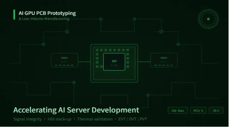
  • How Do AI GPU PCB Prototype and Low-Volume PCB Manufacturing Accelerate AI Server Development?
    Blog

    How Do AI GPU PCB Prototype and Low-Volume PCB Manufacturing Accelerate AI Server Development?

    ByDavid 06/08/202606/12/2026

    AI GPU PCB prototyping and low-volume manufacturing streamline next-generation hardware architecture development by compressing the design-to-validation cycle. This process allows engineering teams to systematically verify signal integrity, manage thermal dissipation boundaries, and evaluate high-density interconnect (HDI) routing structures under real-world operating margins. Why Is Rapid Prototyping Critical for High-Layer AI GPU PCBs? Rapid prototyping mitigates…
    Read More How Do AI GPU PCB Prototype and Low-Volume PCB Manufacturing Accelerate AI Server Development?Continue

  • An abstract 3D technology background featuring illuminating network nodes, glowing data pathways, and interconnected circuit geometric lines. This vector-style digital illustration visualizes complex multi-layer stack-ups, high-density signal interconnects (HDI), and advanced trace routing architectures required for high-speed AI data center server PCBs operating at 112G and 224G PAM4 bandwidth frequencies.
    Blog

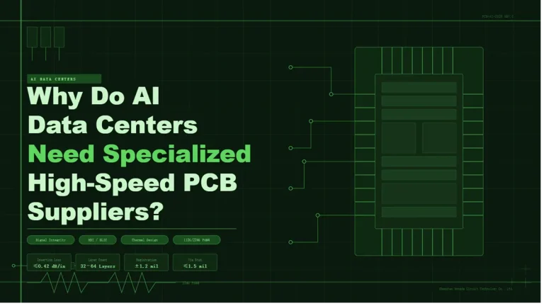
    Why Do AI Data Centers Need Specialized High-Speed PCB Suppliers?

    ByDavid 06/08/202606/12/2026

    AI data centers require specialized high-speed PCB suppliers because standard manufacturers cannot achieve the ultra-low insertion loss (≤ 0.42 dB/inch @ 56 GHz), high-layer-count registration accuracy (≤ ±1.2 mil), and extreme thermal dissipation necessary to sustain uncompromised signal integrity for next-generation 112G/224G PAM4 architectural frameworks. Why Do AI Accelerators Demand Ultra-High Layer Count Layouts? AI…

    Read More Why Do AI Data Centers Need Specialized High-Speed PCB Suppliers?Continue

  • A professional 3D technical illustration showcasing a high-density interconnect (HDI) layer stack-up and complex ball grid array (BGA) escape routing underneath an advanced NVIDIA GPU system board. The design features micro-precision traces, microvias, and an ultra-dense multi-layer printed circuit board topology engineered to support 112G and 224G PAM4 high-speed differential signaling frequencies in AI data center servers.
    Blog

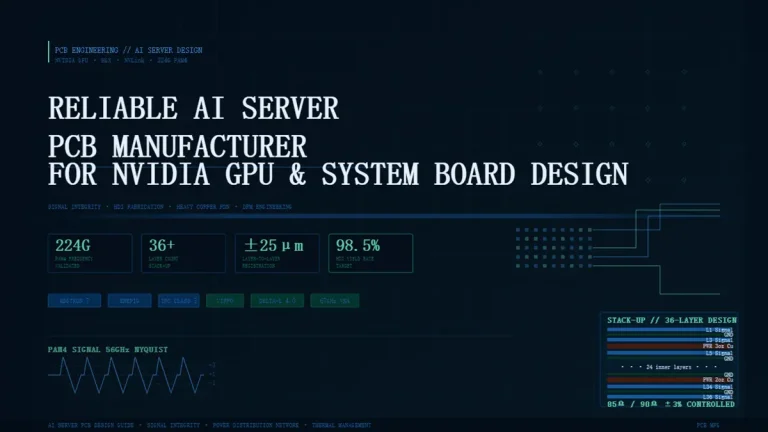
    What Defines a Reliable AI Server PCB Manufacturer for NVIDIA GPU and GPU System Board Design?

    ByDavid 06/06/202606/12/2026

    ditiAs transmission frequencies scale up to 224G PAM4 and hardware designs migrate toward complex multi-GPU cluster architectures, traditional PCB fabrication boundaries are being pushed to their limits. A reliable GPU power-delivery and high-speed PCB manufacturer typically transitions from standard production to an advanced engineering-driven methodology. This requires managing high-layer-count stack-ups (24+ to 36+ layers), heavy-copper…

    Read More What Defines a Reliable AI Server PCB Manufacturer for NVIDIA GPU and GPU System Board Design?Continue

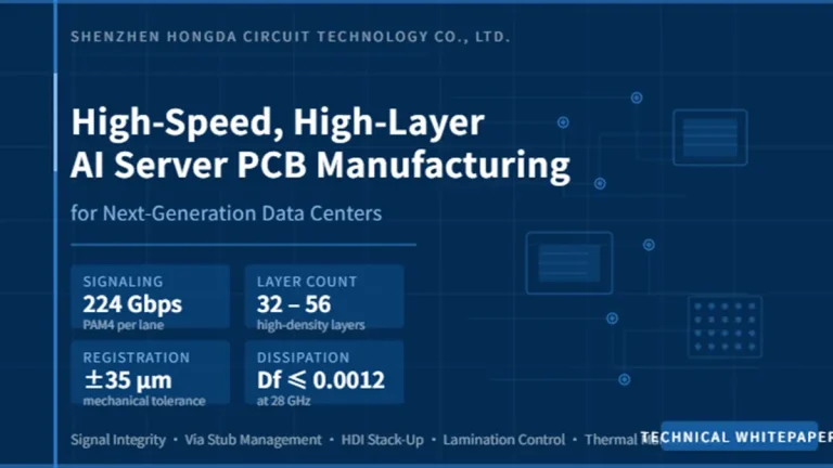
  • Technical whitepaper cover for high-speed, high-layer AI server PCB manufacturing by Shenzhen Hongda Circuit Technology, featuring tech specs of 224 Gbps signaling, 32-56 layer count, plus or minus 35 micrometers registration mechanical tolerance, and Df less than or equal to 0.0012 at 28 GHz.
    Blog

    High-Speed, High-Layer AI Server PCB Manufacturing for Next-Gen Data Centers

    ByDavid 06/05/202606/12/2026

    Next-generation data centers require 224Gbps PAM4 signaling and 32-to-56 high-layer counts to route dense accelerator fabrics. Achieving signal integrity at these thresholds demands strict mechanical registration within ±35μm, ultra-low-loss resin selection, and extreme aspect-ratio via drilling to eliminate high-frequency parasitic stubs and thermal failures under continuous 1200W GPU workloads. How Do Material Dynamics and Resin…

    Read More High-Speed, High-Layer AI Server PCB Manufacturing for Next-Gen Data CentersContinue

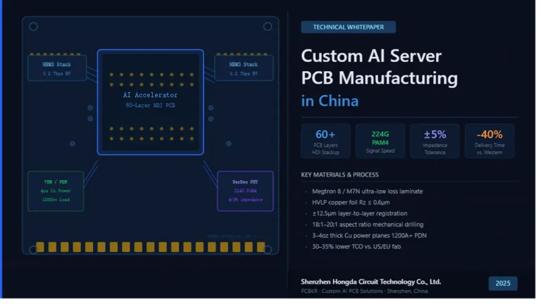
  • Technical whitepaper cover image titled "Custom AI Server PCB Manufacturing in China" by Shenzhen Hongda Circuit Technology Co., Ltd. (PCBKR). Features a blueprint diagram of a 60-layer HDI PCB with AI Accelerator, HBM3 stack, 4oz copper power VRM, and SerDes PHY on the left, and key performance metrics (60+ layers, 224G PAM4, +/-5% impedance tolerance, -40% lead time) on the right.
    Blog

    Custom AI Server PCB Manufacturing in China

    ByDavid 06/05/202606/12/2026

    Shenzhen Hongda Circuit Technology Co., Ltd. (PCBKR) Custom AI Server PCB Manufacturing in China Core Breakdown: China thoroughly dominates the high-layer PCB mass production market by offering core fabrication capabilities for custom AI server PCBs supporting 28 to 60+ layers, utilizing ultra-low loss materials like Megtron 8, and ensuring error-free transmission for 224Gbps PAM4 signaling architectures. Powered by sub-micron…

    Read More Custom AI Server PCB Manufacturing in ChinaContinue

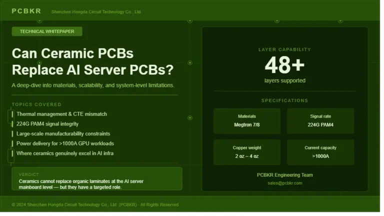
  • Technical whitepaper cover titled 'Can Ceramic PCBs Replace AI Server PCBs?' by PCBKR Shenzhen Hongda Circuit Technology Co., Ltd. The graphic outlines material scaling bottlenecks including 48+ layers support for Megtron 7/8 organic laminates, 224G PAM4 signal rate, 2oz to 4oz copper weight, and greater than 1000A current capacity against thin/co-fired ceramic substrate limitations.
    Blog

    Can Ceramic PCBs Replace AI Server PCBs?

    ByDavid 06/04/202606/12/2026

    No, ceramic PCBs cannot wholesale replace AI server PCBs. While offering superior raw material thermal conductivity, severe structural limitations in multi-layer sequential lamination (>20 layers), ultra-large form factor scaling (>600 mm), multi-phase high-current power delivery (>1000 A), and brittle mechanical failure modes make them completely unviable for mainboard infrastructure. 1. What Are Ceramic PCBs and How…

    Read More Can Ceramic PCBs Replace AI Server PCBs?Continue

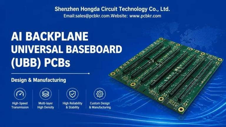
  • AI Universal Baseboard PCB Manufacturing for High-Performance Computing Systems
    Blog

    AI Universal Baseboard (UBB) PCB Manufacturing: Design, Fabrication and OEM Procurement

    ByDavid 06/04/202611/12/2026

    AI Universal Baseboard PCB Manufacturing delivers the high-density circuit foundation required for modern AI compute hardware. An AI Universal Baseboard (UBB) is a high-density printed circuit board used to interconnect accelerator modules, high-speed interfaces, power distribution networks, and other functional elements within AI computing platforms. Manufacturing a UBB requires careful coordination of multilayer stackup design,…

    Read More AI Universal Baseboard (UBB) PCB Manufacturing: Design, Fabrication and OEM ProcurementContinue

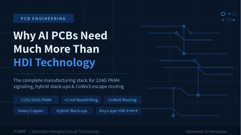
  • Banner image for AI PCB manufacturing article titled "Why AI PCBs Need Much More Than HDI Technology" by Shenzhen Hongda Circuit Technology (PCBKR), highlighting 224G PAM4 signaling and CoWoS routing.
    Blog

    Why AI PCBs Need Much More Than HDI Technology

    ByDavid 06/03/202606/12/2026

    Introduction: The Quantitative Realities of AI Hardware Many procurement managers and hardware designers operate under a significant misconception: they assume an AI Printed Circuit Board (PCB) is merely an upgraded High-Density Interconnect (HDI) board[cite: 1]. While HDI is necessary for routing high-density component footprints, it represents less than 30% of the entire system engineering matrix…

    Read More Why AI PCBs Need Much More Than HDI TechnologyContinue

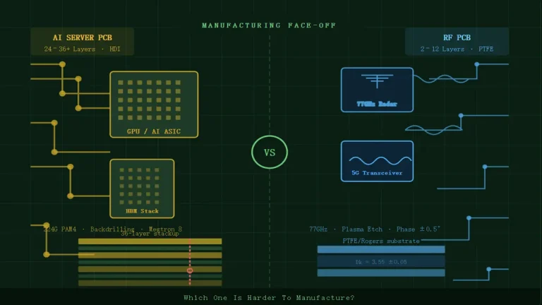
  • alt="Technical comparison diagram between AI Server PCB and RF PCB highlighting layer count, substrate materials, and manufacturing challenges."
    Blog

    AI PCB vs RF PCB: Which One Is Harder To Manufacture?

    ByDavid 06/03/202606/12/2026

    AI PCB vs RF PCB Direct Summary: AI PCBs present a higher cumulative manufacturing difficulty than RF PCBs. While RF boards require extreme localized dielectric uniformity and strict impedance tolerances (±2%) on dedicated paths, high-layer AI PCBs (24–36+ layers) combined with 224G PAM4 architectures, complex multi-stage sequential laminations, and massive Any-Layer HDI densities introduce significantly higher…

    Read More AI PCB vs RF PCB: Which One Is Harder To Manufacture?Continue

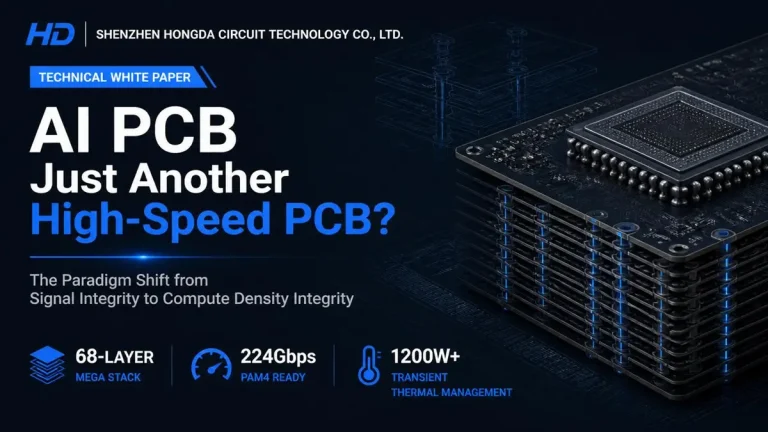
  • Technical whitepaper cover for Shenzhen Hongda Circuit Technology titled "Is AI PCB Just Another High-Speed PCB?", featuring a 3D high-layer count vertical PCB stackup structure, 68 layers mega stack icon, 224Gbps PAM4 ready, and 1200W+ transient thermal management metrics.
    Blog

    Is AI PCB Just Another High-Speed PCB?

    ByDavid 06/02/202606/12/2026

    A Paradigmatic Shift from Signal Integrity to Compute Density Integrity No. AI PCBs represent a multidimensional paradigm shift scaling layers up to 68, driving 224Gbps PAM4 signaling, managing >1200W transient thermal fluxes, and requiring micro-level electro-thermal-mechanical co-design. While traditional high-speed PCBs isolate their focus to signal routing attenuation and impedance tolerances, AI PCBs represent a…

    Read More Is AI PCB Just Another High-Speed PCB?Continue

Page navigation

Previous PagePrevious 1 … 37 38 39 40 41 … 44 Next PageNext

Shenzhen Hongda Circuit Technology Co., Ltd

Address: Room 1608-1610, Research Development Comprehensive Building, Baoyunda Logistics Center, Baoan, Shenzhen, China

E-mail:sales@pcbkr.com

TEL:+86 0755 23720053

Industry Insight Blog

PCB manufacturer

High-Frequency PCB

HDI PCB

Multilayer PCB

Metal Core PCB

High-Speed PCB

Heavy Copper PCB

Flex PCB

Rigid-Flex PCB

IC Substrates PCB

Technology

120-Layer 5G-Advanced/6G Communication Boards

High-Speed Semiconductor Test Boards

mSAP-Processed IC Package Substrates

Specialized Millimeter-Wave Radar PCBs

224Gbps High-Frequency Microwave Circuits

Intelligent Industrial Control PCBs

© 2026 Shenzhen Hongda Circuit Technology Co., Ltd.

  • Home
  • PCB Products
    • High-Frequency PCB
    • HDI PCB
    • Multilayer PCB
    • Metal Core PCB
    • High-Speed PCB
    • Heavy Copper PCB
    • Flex PCB
    • Rigid-Flex PCB
    • IC Substrates PCB
  • PCB Assembly
    •  Advanced BGA & SMT 
    • Box Build & Cable Assy 
    • Component Sourcing
    • Turnkey & Consignment
  • Capability Overview
    • Capability
    • Advanced Equipment
    • PCB Design & Eng.
    • Standard PCB Capability
    • IC Substrate Capability
    • HDI PCB Capability
    • Rigid-Flex Capability
    • RF PCB Capability
    • High frequency PCBs Capability
  • Technology
    • 120-Layer 5G-Advanced/6G Communication Boards
    • High-Speed Semiconductor Test Boards
    • mSAP-Processed IC Package Substrates
    • Specialized Millimeter-Wave Radar PCBs
    • 224Gbps High-Frequency Microwave Circuits
    • Intelligent Industrial Control PCBs
    • FAQ
  • Blog
  • About Us
    • Certifications
  • Contact