Skip to content
PCBkr.com
  • Home
  • PCB ProductsExpand
    • High-Frequency PCB
    • HDI PCB
    • Multilayer PCB
    • Metal Core PCB
    • High-Speed PCB
    • Heavy Copper PCB
    • Flex PCB
    • Rigid-Flex PCB
    • IC Substrates PCB
  • PCB AssemblyExpand
    •  Advanced BGA & SMT 
    • Box Build & Cable Assy 
    • Component Sourcing
    • Turnkey & Consignment
  • Capability OverviewExpand
    • Capability
    • Advanced Equipment
    • PCB Design & Eng.
    • Standard PCB Capability
    • IC Substrate Capability
    • HDI PCB Capability
    • Rigid-Flex Capability
    • RF PCB Capability
    • High frequency PCBs Capability
  • TechnologyExpand
    • 120-Layer 5G-Advanced/6G Communication Boards
    • High-Speed Semiconductor Test Boards
    • mSAP-Processed IC Package Substrates
    • Specialized Millimeter-Wave Radar PCBs
    • 224Gbps High-Frequency Microwave Circuits
    • Intelligent Industrial Control PCBs
    • FAQ
  • Blog
  • About UsExpand
    • Certifications
  • Contact
  • AI Server Backplane PCB Manufacturer for 224G PAM4 and HDI multilayer backplanes
    Blog

    AI Server Backplane PCB Manufacturer: 224G HDI Manufacturing for OEMs

    ByDavid 05/27/202611/16/2026

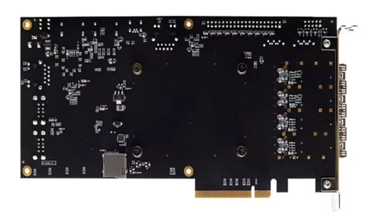
    An AI Server Backplane PCB Manufacturer must be capable of producing high-density, multilayer backplanes that maintain reliable electrical performance across high-speed computing, storage, switching, and power subsystems. As AI servers and accelerator platforms adopt increasingly demanding signal architectures, backplane manufacturing requires more than achieving a specified layer count or minimum trace width. For 224G PAM4…

    Read More AI Server Backplane PCB Manufacturer: 224G HDI Manufacturing for OEMsContinue

  • Ultra-HDI PCB manufacturing for AI server applications, showing multilayer high-density circuit board fabrication and fine-line copper structures.
    Blog

    Ultra-HDI PCB Manufacturing: Critical Bottlenecks in AI Server Production

    ByDavid 05/26/202611/13/2026

    AI server hardware is increasing demand for Ultra-HDI PCB structures that support dense component escape routing, multilayer interconnections, and increasingly demanding manufacturing tolerances. However, achieving fine-line geometry on a design file does not automatically translate into reliable production. The main challenges involve copper pattern formation, laser microvia processing, interlayer registration, sequential lamination, and inspection. For…

    Read More Ultra-HDI PCB Manufacturing: Critical Bottlenecks in AI Server ProductionContinue

  • What PCB Technologies Are Used in AI Data Centers
    Blog

    What PCB Technologies Are Used in AI Data Centers?

    ByDavid 05/25/202606/12/2026

    AI data centers rely on ultra-high-layer-count PCBs, low-loss materials, HDI structures, advanced backdrilling, high-current copper designs, and 112G/224G PAM4 architectures to support GPU clusters exceeding 800G networking bandwidth and 1000A power delivery requirements. Why Do AI Data Centers Require Completely Different PCB Technologies? AI data center PCBs operate under dramatically higher bandwidth, current density, and…

    Read More What PCB Technologies Are Used in AI Data Centers?Continue

  • Why Are AI Server PCBs More Expensive Than Traditional PCBs
    Blog

    Why Are AI Server PCBs More Expensive Than Traditional PCBs?

    ByDavid 05/24/202606/12/2026

    AI server PCBs are dramatically more expensive because they combine ultra-high-speed signaling, extreme power density, advanced materials, complex multilayer manufacturing, and much stricter reliability requirements than conventional PCBs. In many real-world deployments, AI server boards cost 3–10× more than traditional server PCBs due to compounded engineering and fabrication challenges. As AI infrastructure expands globally, PCB…

    Read More Why Are AI Server PCBs More Expensive Than Traditional PCBs?Continue

  • Why Do AI Server PCBs Require More Testing?
    Blog

    Why Do AI Server PCBs Require More Testing?

    ByDavid 05/24/202606/12/2026

    AI server PCBs require far more testing because they operate under extreme current density, ultra-high-speed PAM4 signaling, continuous thermal cycling, and synchronized multi-GPU workloads. A microscopic PCB defect that would be harmless in traditional servers can trigger AI training collapse, GPU desynchronization, packet retransmission storms, or catastrophic cluster instability. Why Are AI Server PCB Failure…

    Read More Why Do AI Server PCBs Require More Testing?Continue

  • high-layer-count-ai-motherboard
    Blog

    Why Are AI Server PCBs Harder to Manufacture?

    ByDavid 05/23/202606/12/2026

    AI server PCBs are harder to manufacture because they simultaneously demand ultra-high layers (20–36+), 112G/224G PAM4 signaling, massive 1000A+ current delivery, and micron-level tolerances. Achieving this forces manufacturers to mix ultra-low-loss materials and heavy copper, where any microscopic fabrication deviation triggers immediate signal collapse or catastrophic thermal runaway. Why Do AI Server PCBs Require Much…

    Read More Why Are AI Server PCBs Harder to Manufacture?Continue

  • Custom high layer count PCB prototyping with complex 24–36 layer multilayer circuit board stackup
    Blog

    Custom High Layer Count PCB Prototyping for 24–36+ Layer Designs

    ByDavid 05/22/202611/11/2026

    Custom high layer count PCB prototyping requires more than adding additional copper layers to a conventional multilayer board. As layer counts increase, prototype manufacturing becomes more sensitive to stackup symmetry, dielectric thickness, lamination cycles, interlayer registration, drilling accuracy, and electrical performance. Shenzhen Hongda Circuit Technology Co., Ltd. (PCBKR) provides custom multilayer PCB fabrication and engineering…

    Read More Custom High Layer Count PCB Prototyping for 24–36+ Layer DesignsContinue

  • Capability for high-density, high-layer-count PCB fabrication
    Blog

    Why Is Signal Integrity More Difficult in AI Server PCBs?

    ByDavid 05/21/202606/12/2026

    Signal integrity in AI server PCBs is difficult because 112G/224G PAM4 channels are now dominated less by routing topology and more by production-induced electromagnetic variability, including dielectric phase drift, copper morphology dispersion, via resonance instability, thermal-mechanical deformation, and local manufacturing nonuniformity that conventional PCB process windows cannot statistically control. Why Do 112G/224G PAM4 AI Channels…

    Read More Why Is Signal Integrity More Difficult in AI Server PCBs?Continue

  • Why Do AI Server PCBs Require 20+ Layers
    Blog

    Why Do AI Server PCBs Require 20+ Layers?

    ByDavid 05/19/202606/12/2026

    Professional Technical Article | AI Data Center Hardware PCB Research AI server PCBs need 20+ layers to meet high-speed signaling (PCIe 5.0/6.0), high-current power delivery (350–700W per GPU), and dense interconnects, while ensuring signal integrity, thermal dissipation, and manufacturing scalability. Why Is 20+ Layers Mandatory for High-Speed AI Signaling? PCIe 5.0 (32 GT/s) and PCIe…

    Read More Why Do AI Server PCBs Require 20+ Layers?Continue

  • PCIe 6.0 PCB Materials comparing low-loss Megtron, FR-4 and PTFE laminates for high-speed multilayer PCB manufacturing.
    Blog

    Which PCB Materials Can Replace Standard FR-4 for PCIe 6.0?

    ByDavid 05/18/202611/11/2026

    PCIe 6.0 PCB Materials selection is critical because PCIe 6.0 operates at 64 GT/s using PAM4 signaling, which places growing emphasis on PCB dielectric loss, copper roughness, impedance consistency and overall channel design. For AI servers, accelerator cards and high-speed computing platforms, migrating from standard FR-4 to a properly selected low-loss laminate helps retain signal…

    Read More Which PCB Materials Can Replace Standard FR-4 for PCIe 6.0?Continue

Page navigation

Previous PagePrevious 1 … 39 40 41 42 43 44 Next PageNext

Shenzhen Hongda Circuit Technology Co., Ltd

Address: Room 1608-1610, Research Development Comprehensive Building, Baoyunda Logistics Center, Baoan, Shenzhen, China

E-mail:sales@pcbkr.com

TEL:+86 0755 23720053

Industry Insight Blog

PCB manufacturer

High-Frequency PCB

HDI PCB

Multilayer PCB

Metal Core PCB

High-Speed PCB

Heavy Copper PCB

Flex PCB

Rigid-Flex PCB

IC Substrates PCB

Technology

120-Layer 5G-Advanced/6G Communication Boards

High-Speed Semiconductor Test Boards

mSAP-Processed IC Package Substrates

Specialized Millimeter-Wave Radar PCBs

224Gbps High-Frequency Microwave Circuits

Intelligent Industrial Control PCBs

© 2026 Shenzhen Hongda Circuit Technology Co., Ltd.

  • Home
  • PCB Products
    • High-Frequency PCB
    • HDI PCB
    • Multilayer PCB
    • Metal Core PCB
    • High-Speed PCB
    • Heavy Copper PCB
    • Flex PCB
    • Rigid-Flex PCB
    • IC Substrates PCB
  • PCB Assembly
    •  Advanced BGA & SMT 
    • Box Build & Cable Assy 
    • Component Sourcing
    • Turnkey & Consignment
  • Capability Overview
    • Capability
    • Advanced Equipment
    • PCB Design & Eng.
    • Standard PCB Capability
    • IC Substrate Capability
    • HDI PCB Capability
    • Rigid-Flex Capability
    • RF PCB Capability
    • High frequency PCBs Capability
  • Technology
    • 120-Layer 5G-Advanced/6G Communication Boards
    • High-Speed Semiconductor Test Boards
    • mSAP-Processed IC Package Substrates
    • Specialized Millimeter-Wave Radar PCBs
    • 224Gbps High-Frequency Microwave Circuits
    • Intelligent Industrial Control PCBs
    • FAQ
  • Blog
  • About Us
    • Certifications
  • Contact