Skip to content
PCBkr.com
  • Home
  • PCB ProductsExpand
    • High-Frequency PCB
    • HDI PCB
    • Multilayer PCB
    • Metal Core PCB
    • High-Speed PCB
    • Heavy Copper PCB
    • Flex PCB
    • Rigid-Flex PCB
    • IC Substrates PCB
  • PCB AssemblyExpand
    •  Advanced BGA & SMT 
    • Box Build & Cable Assy 
    • Component Sourcing
    • Turnkey & Consignment
  • Capability OverviewExpand
    • Capability
    • Advanced Equipment
    • PCB Design & Eng.
    • Standard PCB Capability
    • IC Substrate Capability
    • HDI PCB Capability
    • Rigid-Flex Capability
    • RF PCB Capability
    • High frequency PCBs Capability
  • TechnologyExpand
    • 120-Layer 5G-Advanced/6G Communication Boards
    • High-Speed Semiconductor Test Boards
    • mSAP-Processed IC Package Substrates
    • Specialized Millimeter-Wave Radar PCBs
    • 224Gbps High-Frequency Microwave Circuits
    • Intelligent Industrial Control PCBs
    • FAQ
  • Blog
  • About UsExpand
    • Certifications
  • Contact
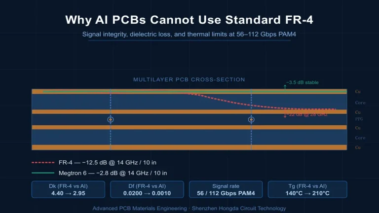
  • Why AI PCBs cannot use standard FR-4 materials: insertion loss comparison between FR-4 and Megtron 6 at 14GHz by Shenzhen Hongda Circuit Technology.
    Blog

    Why AI PCBs Cannot Use Standard FR-4 Materials

    ByDavid 06/02/202606/12/2026

    Standard FR-4 materials fail in AI PCBs because their high dielectric constant (Dk) and dissipation factor (Df) cause catastrophic signal attenuation and bit errors at ultra-high frequencies (56Gbps/112Gbps PAM4), rendering them incapable of handling the extreme data rates and thermal loads required by AI clusters. Why Do AI Training Servers Demand Alternative Substrates Over FR-4?…
    Read More Why AI PCBs Cannot Use Standard FR-4 MaterialsContinue

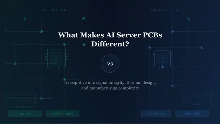
  • AI Server PCB vs Traditional PCB technical specifications comparison chart banner
    Blog

    What Makes AI Server PCBs Different From Traditional Enterprise PCBs?

    ByDavid 06/01/202606/12/2026

    The global shift toward high-performance computing and artificial intelligence infrastructure has sparked a major technological evolution in data center hardware. When analyzing the core infrastructure supporting this revolution, evaluating the engineering requirements of an AI Server PCB vs. Traditional PCB architecture reveals a massive technical chasm. As generative AI models grow exponentially, traditional enterprise server motherboards can…

    Read More What Makes AI Server PCBs Different From Traditional Enterprise PCBs?Continue

  • How to Choose an AI Backplane PCB Manufacturer — A complete buyer's and engineering guide covering material selection, signal integrity, 112G/224G PAM4 requirements, and IPC Class 3 standards for high-speed data center infrastructure.
    Blog

    How to Choose an AI Backplane PCB Manufacturer: The Ultimate Buyer’s & Engineering Guide

    ByDavid 06/01/202606/12/2026

    Finding a highly capable AI Backplane PCB Manufacturer is one of the most mission-critical decisions for hardware engineers and procurement professionals deploying next-generation data center infrastructure. As high-performance computing clusters scale, selecting an experienced AI Backplane PCB Manufacturer directly dictates whether your system successfully hits its error-free bandwidth targets or suffers from catastrophic signal degradation. In the era of…

    Read More How to Choose an AI Backplane PCB Manufacturer: The Ultimate Buyer’s & Engineering GuideContinue

  • AI server PCB layer count showing high-layer-count multilayer PCB manufacturing for GPU and high-speed computing systems
    Blog

    Why Do AI Servers Require More PCB Layers, and How Many Are Needed?

    ByDavid 05/31/202611/10/2026

    AI servers require higher PCB layer counts because GPU accelerators, high-bandwidth memory, high-speed interconnects, and demanding power distribution networks compete for limited routing space. The required layer count depends on component density, signal routing, power integrity, stackup design, and mechanical constraints—not simply on the processor’s performance rating. For hardware developers and OEM procurement teams, selecting…

    Read More Why Do AI Servers Require More PCB Layers, and How Many Are Needed?Continue

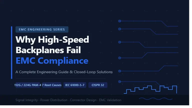
  • Why High-Speed Backplanes Fail EMC Compliance
    Blog

    Why High-Speed Backplanes Fail EMC Compliance

    ByDavid 05/30/202606/12/2026

    Table of Contents Why High-Speed Backplanes Frequently Fail EMC Compliance Testing: A Complete Engineering Guide and Closed-Loop Solutions I. Executive Summary and Industry Compliance Overview In modern digital infrastructure, high-speed backplanes serve as the physiological backbone interconnecting various daughter cards within core hardware systems. However, because these backplanes are physically large, densely routed, and exhibit…

    Read More Why High-Speed Backplanes Fail EMC ComplianceContinue

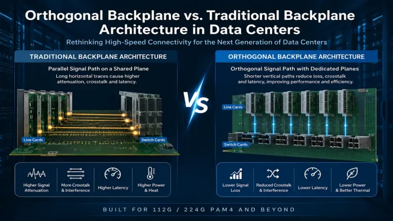
  • Comparison of Orthogonal Backplane PCB and traditional architecture showing signal paths for 112G and 224G PAM4 data centers.
    Blog

    What is the difference between an orthogonal backplane and a traditional backplane architecture in data centers?

    ByDavid 05/30/202606/12/2026

    In the hardware development of next-generation data center clusters, optimizing copper interconnect topologies to mitigate extreme high-speed signal attenuation has become a critical challenge shared by system architects and procurement decision-makers. With the broad adoption of 112G PAM4 signaling and the sequential transition toward 224G PAM4 architectures, deploying a high-performance Orthogonal Backplane PCB design is demonstrating superior…

    Read More What is the difference between an orthogonal backplane and a traditional backplane architecture in data centers?Continue

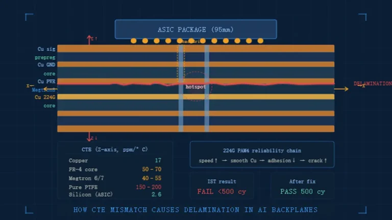
  • Cross-section diagram of an AI Backplane showing CTE mismatch and delamination risks under a 95mm ASIC package during thermal cycling.
    Blog

    How CTE Mismatch Causes Delamination in AI Backplanes

    ByDavid 05/29/202606/12/2026

    AI Backplanes operate under extreme thermal cycling, high current density, and ultra-low-loss material requirements. In modern AI Backplanes, CTE mismatch between copper, resin systems, glass fabric, and large BGA packages is one of the leading root causes of delamination, barrel cracking, CAF risk, and long-term reliability failure. What Is CTE Mismatch in AI Backplanes? The Root…

    Read More How CTE Mismatch Causes Delamination in AI BackplanesContinue

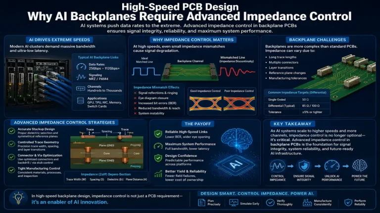
  • High-Speed PCB Design: Why AI Backplanes Require Advanced Impedance Control
    Blog

    High-Speed PCB Design: Why AI Backplanes Require Advanced Impedance Control

    ByDavid 05/29/202606/12/2026

    Technical Insights into High-Speed PCB Signal Integrity for Next-Generation AI Server Infrastructure Table of Contents 1. Introduction: The Critical Role of AI Server Backplanes The explosive global expansion of generative AI, large language models (LLMs), and hyper-scale neural network training workloads has fundamentally disrupted hardware architecture. Traditional data center infrastructures are no longer capable of…

    Read More High-Speed PCB Design: Why AI Backplanes Require Advanced Impedance ControlContinue

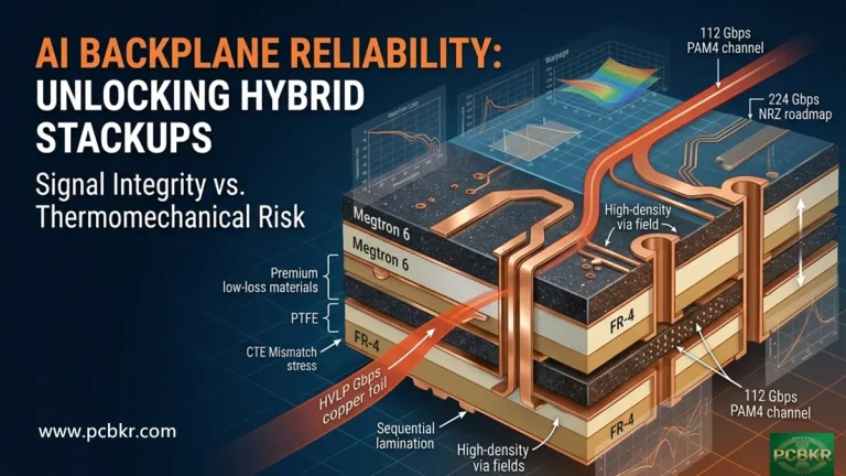
  • A technical 3D illustration demonstrating AI backplane reliability and hybrid PCB stackups. The diagram shows multiple layers including Megtron 6, PTFE, and FR-4, along with copper traces, high-density via fields, and data charts for insertion loss and warpage under 112 Gbps and 224 Gbps roadmaps.
    Blog

    How Hybrid Stackups Affect AI Backplane Reliability

    ByDavid 05/28/202606/12/2026

    Hybrid stackups — combining low-loss laminates (PPE/PPO-based Megtron 6, or true PTFE) with FR-4 — improve 112 Gbps+ AI backplane signal integrity but introduce CTE-mismatch delamination risk up to 40% higher than all-FR-4 builds. Copper foil roughness and fiber weave effects further complicate reliability. Correct material classification, sequential lamination planning, and per-layer simulation are mandatory…

    Read More How Hybrid Stackups Affect AI Backplane ReliabilityContinue

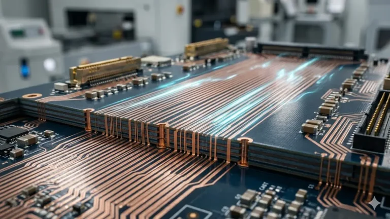
  • A macro photograph of a 48-layer 224G AI backplane PCB in dark blue and grey. The image highlights hundreds of parallel copper traces, exposed cross-sections showing multiple circuit layers, and clean laser-drilled vias. Soft blue light pulses simulate high-frequency 56GHz PAM4 data streams traveling along the circuits under professional cleanroom studio lighting.
    Blog

    How 224G PAM4 Changes AI Backplane PCB Design?

    ByDavid 05/27/202606/12/2026

    How 224G PAM4 Changes AI Backplane PCB Design? The relentless rise of generative AI clusters has pushed data center architectures to their absolute physical limits, forcing a rapid transition toward 224G PAM4 PCB infrastructure. As next-generation AI servers demand unprecedented bandwidth to process massive LLMs (Large Language Models), the industry is moving away from 112G NRZ/PAM4 signaling,…

    Read More How 224G PAM4 Changes AI Backplane PCB Design?Continue

Page navigation

Previous PagePrevious 1 … 38 39 40 41 42 … 44 Next PageNext

Shenzhen Hongda Circuit Technology Co., Ltd

Address: Room 1608-1610, Research Development Comprehensive Building, Baoyunda Logistics Center, Baoan, Shenzhen, China

E-mail:sales@pcbkr.com

TEL:+86 0755 23720053

Industry Insight Blog

PCB manufacturer

High-Frequency PCB

HDI PCB

Multilayer PCB

Metal Core PCB

High-Speed PCB

Heavy Copper PCB

Flex PCB

Rigid-Flex PCB

IC Substrates PCB

Technology

120-Layer 5G-Advanced/6G Communication Boards

High-Speed Semiconductor Test Boards

mSAP-Processed IC Package Substrates

Specialized Millimeter-Wave Radar PCBs

224Gbps High-Frequency Microwave Circuits

Intelligent Industrial Control PCBs

© 2026 Shenzhen Hongda Circuit Technology Co., Ltd.

  • Home
  • PCB Products
    • High-Frequency PCB
    • HDI PCB
    • Multilayer PCB
    • Metal Core PCB
    • High-Speed PCB
    • Heavy Copper PCB
    • Flex PCB
    • Rigid-Flex PCB
    • IC Substrates PCB
  • PCB Assembly
    •  Advanced BGA & SMT 
    • Box Build & Cable Assy 
    • Component Sourcing
    • Turnkey & Consignment
  • Capability Overview
    • Capability
    • Advanced Equipment
    • PCB Design & Eng.
    • Standard PCB Capability
    • IC Substrate Capability
    • HDI PCB Capability
    • Rigid-Flex Capability
    • RF PCB Capability
    • High frequency PCBs Capability
  • Technology
    • 120-Layer 5G-Advanced/6G Communication Boards
    • High-Speed Semiconductor Test Boards
    • mSAP-Processed IC Package Substrates
    • Specialized Millimeter-Wave Radar PCBs
    • 224Gbps High-Frequency Microwave Circuits
    • Intelligent Industrial Control PCBs
    • FAQ
  • Blog
  • About Us
    • Certifications
  • Contact