Embedded Component PCB: Technology, Manufacturing & Procurement Guide
What Is an Embedded Component PCB?
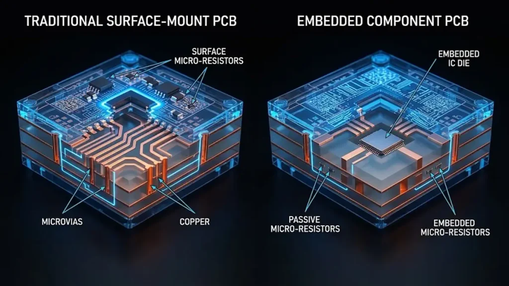
3D Cross-Section Comparison: Traditional Surface-Mount PCB vs. Embedded Component PCB
An Embedded Component PCB is a printed circuit board in which selected passive or active electronic components are integrated within the PCB structure rather than mounted entirely on the outer surface. This approach can save board space, shorten electrical paths, reduce parasitic effects and increase functional density.
Unlike a conventional PCB, where most components are placed on the top or bottom surface using SMT or through-hole assembly, an embedded component PCB uses part of the internal PCB structure as an integration space.
Typical embedded components include:
- Embedded resistors
- Embedded capacitors
- Embedded inductors
- Embedded passive networks
- Embedded ICs
- Embedded dies
- Other active or passive devices
IPC documentation recognizes embedded passive and active circuitry as an established PCB technology area, while IPC-7092 specifically addresses design and assembly implementation for embedded circuitry.
For engineering and procurement teams, the important question is not simply whether a supplier can manufacture an embedded PCB. The real question is whether the manufacturer can control component placement, cavity geometry, lamination, microvias, copper filling, registration, thermal stress and electrical reliability as one integrated manufacturing process.
That distinction is critical when selecting an Embedded Component PCB Manufacturer.
What Types of Components Can Be Embedded in a PCB?
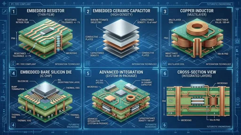
Infographic Grid Display: Types of Embedded PCB Components and Integration Structures
Embedded Resistor PCB
Embedded resistors can be integrated into inner PCB layers using dedicated resistive materials or embedded resistor structures. Embedded passive components in PCB covers full‑depth design, material and manufacturing guidance for resistor, capacitor and inductor embedding.
This can eliminate selected discrete components from the surface and provide more available space for connectors, ICs and other components.
Embedded Capacitor PCB
Embedded capacitors are particularly useful when decoupling or high-frequency power integrity is important.
Placing capacitance closer to the active device can reduce the electrical path between the power source and load. IPC’s embedded passive technology documentation identifies capacitors, resistors and inductors as common passive component categories for embedded implementation.
Embedded Inductor PCB
Embedded inductors can be used in selected RF, power-management and filtering applications where electromagnetic performance and available board space must be balanced.
Embedded Active Components PCB
Active devices can also be embedded in suitable PCB or substrate structures.
However, active-component embedding introduces substantially greater process complexity than embedding simple passive structures because thermal dissipation, component protection, interconnection, warpage and reliability must be evaluated together.
Embedded Die PCB
Die embedding represents a more advanced form of component integration.
Instead of mounting a packaged component on the PCB surface, a bare die or semiconductor device may be integrated into an internal structure and interconnected using microvia, redistribution or other fine-pitch technologies.
This moves the PCB closer to the boundary between conventional printed circuit fabrication and advanced electronic packaging.
How Are Embedded Components Integrated Inside a PCB?
Cavity Embedded Component Technology
One common approach uses a precisely controlled cavity to accommodate the component.
The cavity must provide sufficient dimensional clearance while maintaining mechanical stability during lamination.
For procurement teams, cavity depth tolerance and registration capability should therefore be evaluated alongside the nominal component dimensions.
Component Placement and Internal Registration
The embedded component must be positioned relative to the PCB reference system.
Small registration errors can create problems when subsequent laser drilling, via formation and outer-layer routing are performed.
This is one reason why embedded component PCB manufacturing is closely connected with modern LDI, laser drilling and automated registration technology.
Sequential Lamination
Sequential lamination is frequently important for complex embedded component structures.
The manufacturing sequence may include:
DFM → Material Selection → Inner Layer Circuit → Cavity → Component Placement → Lamination → Laser Drilling → Plating → Routing → Surface Finish → Inspection → Electrical Test
This manufacturing flow follows the core process structure identified in the supplied technical outline. Embedded Component PCB Manufacturing Process: Step‑by‑Step Guide breaks down each fabrication stage with detailed process controls and comparison data
Microvias and Copper Filling
Modern embedded component PCBs increasingly require HDI structures.
Laser microvias can provide electrical connections between build-up layers while minimizing the area consumed by conventional through-hole vias.
For higher-density designs, stacked or staggered microvias may be combined with via-in-pad and copper-filled structures.
This is where Embedded Component PCB Manufacturing increasingly overlaps with advanced HDI and substrate-like PCB technology.
Why Does Embedded Component PCB Technology Matter?
The major change in PCB manufacturing is not simply smaller line widths.
The industry is moving toward greater integration among:
- HDI
- mSAP
- laser microvias
- fine-line routing
- low-loss materials
- embedded components
- advanced packaging
- automated inspection
- high-speed electrical validation
Modern manufacturing equipment is therefore becoming a direct determinant of whether a supplier can economically manufacture advanced embedded structures.
For example, Hongda’s published manufacturing capabilities include LDI equipment, Mitsubishi UV/CO₂ laser drilling, automated plating, fine-line mSAP processing and advanced microvia manufacturing.
The practical implication for buyers is simple:
The supplier’s equipment architecture can directly influence the achievable density, registration accuracy, microvia reliability, yield and ultimately the cost of an Embedded Component PCB.
How Does Advanced PCB Manufacturing Equipment Affect Embedded Component PCB Performance?
LDI Improves Fine-Line Registration
Laser Direct Imaging is increasingly important for high-density PCB structures because it avoids the mechanical limitations associated with conventional phototools.
Hongda publicly lists SCREEN LDI capability with high registration accuracy for fine-line and Any-Layer HDI manufacturing.
For embedded component PCB production, better registration can help control:
- Component-to-cavity alignment
- Pad positioning
- Microvia registration
- Fine-line routing
- Layer-to-layer accuracy
This becomes increasingly important as PCB geometries shrink.
UV and CO₂ Laser Drilling Enable Smaller Interconnections
Mechanical drilling becomes increasingly difficult as via diameter decreases.
Hongda’s published capability includes Mitsubishi UV/CO₂ hybrid laser drilling for microvias, while its advanced laser infrastructure also includes picosecond/femtosecond laser technology for specialized applications.
For an embedded component PCB, laser technology can influence:
- Via diameter
- Positional accuracy
- Heat-affected area
- Microvia aspect ratio
- Build-up layer density
- Interconnection reliability
mSAP Supports Fine-Line Embedded PCB Structures
Modified Semi-Additive Processing is particularly valuable where conventional subtractive etching cannot maintain the required fine geometry.
Hongda’s published mSAP capability includes 8/8 μm-class fine-line processing for advanced substrate-like applications.
For buyers, mSAP should not be treated simply as a marketing term.
Ask the manufacturer:
- What line/space can be qualified in production?
- What copper thickness is associated with that geometry?
- What is the actual registration tolerance?
- What is the production yield?
- Can the supplier provide cross-section evidence?
- Is the capability available for prototypes as well as mass production?
Automated AOI and X-Ray Improve Process Visibility
Embedded structures are difficult to inspect because some critical features are physically hidden inside the board.
That increases the value of:
- AOI
- 3D inspection
- X-ray inspection
- Cross-section analysis
- Electrical testing
- Process traceability
Hongda’s published manufacturing information describes 3D AOI and X-ray inspection capabilities for advanced PCB structures.
The key procurement issue is therefore not simply “Does the supplier have AOI?”
A better question is:
“Can the supplier detect defects that are invisible from the PCB surface?”
What Are the Main Benefits of an Embedded Component PCB?
Miniaturization and Space Saving
Embedding selected components frees surface area.
This is particularly valuable for:
- Wearable electronics
- Automotive electronics
- Medical devices
- Compact industrial controls
- High-density communication equipment
- High-performance computing hardware
The supplied technical structure identifies miniaturization and space saving as two of the principal benefits of embedded component PCB technology.
Reduced Parasitic Inductance
A conventional surface-mounted component may require a longer electrical path between the component and the circuit.
Embedding can reduce interconnection length.
For high-speed and high-frequency designs, this can contribute to better electrical behavior.
Improved Signal Integrity
As data rates increase, interconnection geometry becomes increasingly important.
Embedded components can reduce selected electrical path lengths and may help engineers manage parasitic inductance and capacitance.
However, embedded technology should not automatically be interpreted as guaranteeing better signal integrity. Stack-up, dielectric properties, copper roughness, impedance control and routing geometry remain critical.
EMI Reduction
A more integrated internal structure can provide additional opportunities for controlling unwanted electromagnetic coupling.
The final result depends on the complete stack-up and grounding architecture rather than the embedded component alone.
Higher Functional Density
The most important advantage for many applications is not simply making the PCB smaller.
It is increasing the amount of functionality that can be implemented within the same mechanical envelope.
Embedded Component PCB vs Conventional SMT PCB: What Is the Difference?
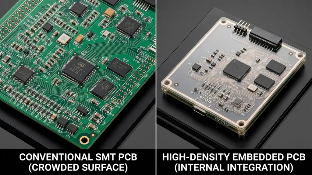
Side-by-Side Comparison: Crowded Conventional SMT PCB vs. High-Density Embedded Component PCB
| Parameter | Embedded Component PCB | Conventional SMT PCB |
|---|---|---|
| Component location | Inside PCB structure and/or surface | Mainly PCB surface |
| Surface area | Reduced component footprint | Larger component footprint |
| Integration density | High | Moderate to high |
| Parasitic path | Can be shorter | Often longer |
| Manufacturing complexity | High | Lower |
| Inspection | More challenging | Easier |
| Repairability | More difficult | Easier |
| DFM requirements | More demanding | More standardized |
| Initial engineering cost | Usually higher | Usually lower |
| Potential miniaturization | Excellent | Good |
| Thermal design | Requires detailed analysis | More straightforward |
| Procurement qualification | More stringent | Relatively straightforward |
The important procurement conclusion is that Embedded Component PCB is not simply a smaller conventional PCB.
It is a different manufacturing strategy. Embedded Component PCB Assembly: Engineering and Manufacturing Guide explores assembly workflows, inspection challenges and hybrid SMT‑embedded process qualification.
What Are the Main Embedded Component PCB Design Challenges?
Stack-Up Design
The stack-up must account for:
- Embedded component position
- Dielectric thickness
- Copper thickness
- Microvia structure
- Impedance
- Thermal expansion
- Lamination pressure
IPC’s standards ecosystem includes guidance covering embedded circuitry, HDI and high-speed PCB design.
Cavity Design
Cavity dimensions must account for:
- Component tolerance
- Adhesive or dielectric material
- Lamination flow
- Clearance
- Mechanical stress
Thermal Management
Embedding a heat-generating component inside a PCB can make heat removal more difficult.
Therefore, thermal vias, copper planes, heat spreaders and material selection must be considered at the design stage.
Signal Integrity
For high-speed applications, engineers should evaluate:
- Controlled impedance
- Via discontinuities
- Dielectric Dk/Df
- Copper roughness
- Return path
- Crosstalk
- Insertion loss
- Reflection
DFM
DFM is one of the most important differences between conventional PCB procurement and embedded component PCB procurement.
A design that is electrically correct may still be difficult to manufacture economically.
That is why early DFM engagement can prevent:
- Excessive cavity tolerances
- Unnecessary microvia structures
- Poor lamination designs
- Low production yield
- Difficult inspection requirements
- Unexpected tooling costs
- Embedded Component PCB Quality Control: An Advanced Manufacturing and Inspection Guide outlines full‑process quality control from incoming material, cavity machining, lamination through lot traceability for embedded‑component constructions.
How Does Embedded Component PCB Manufacturing Affect Cost?
Layer Count
More layers generally increase material, lamination and process complexity.
Embedded Component Type
A simple embedded passive structure is fundamentally different from an embedded active device or die.
Cavity Requirements
Precision cavity machining adds process steps and inspection requirements.
Laser Drilling
Smaller microvias and more complicated via structures increase equipment time and process control requirements.
Material Selection
High-Tg, low-loss and specialized dielectric materials can increase material cost.
Yield
Yield is often more important than the nominal piece price.
A supplier quoting a lower unit price but producing significantly lower first-pass yield may create a higher total cost of ownership.
Testing
Hidden internal structures require more sophisticated inspection and testing.
The supplied procurement framework specifically identifies layer count, materials, component type, cavity, drilling, via technology, yield, testing and volume as major embedded PCB cost factors.
How Should Procurement Teams Evaluate an Embedded Component PCB Manufacturer?
This is where the purchasing decision becomes different from buying a conventional PCB.
1. Manufacturing Capability
Ask whether the supplier has actual production experience with:
- Embedded passive components
- Embedded active components
- Cavities
- Sequential lamination
- HDI
- Laser microvias
- Copper filling
- Fine-line PCB
- mSAP
2. DFM Engineering Support
A strong Embedded Component PCB Manufacturer should review the design before quoting.
The supplier should be able to identify manufacturability risks rather than simply return a price.
3. Prototype Capability
Prototype production is particularly important because embedded structures often require process optimization before mass production. Embedded Component PCB Prototype: From Design Validation to Production covers prototype validation, DFM, tolerance stacking and prototype‑to‑production transfer workflows in depth.
4. Production Capacity
Ask whether the same process used for prototypes can be transferred into stable volume manufacturing.
5. Quality System
Procurement teams should evaluate:
- Quality certifications
- Inspection equipment
- Traceability
- Cross-section capability
- Electrical testing
- X-ray inspection
- Reliability testing
6. Yield Transparency
Yield is one of the most valuable questions procurement can ask.
Instead of asking:
“Can you make this PCB?”
ask:
“What production yield do you normally achieve for this type of structure?”
That question separates laboratory capability from manufacturing capability.
7. Engineering Support
The best supplier should participate before purchase order release.
This reduces the risk of discovering manufacturing problems after tooling and material procurement have already started.
What Should Buyers Include in an Embedded Component PCB RFQ?
A professional RFQ should include:
- Gerber or ODB++ files
- BOM
- Stack-up
- Component specifications
- PCB dimensions
- Layer count
- Embedded component locations
- Cavity dimensions
- Material requirements
- Copper thickness
- Via structure
- Surface finish
- Impedance requirements
- Quantity
- Prototype quantity
- Annual production volume
- Application
- Reliability requirements
- Testing requirements
The original procurement framework also recommends providing Gerber, BOM, stack-up, component specification, quantity, application, reliability and testing requirements when requesting an embedded component PCB quotation.
What Is the Embedded Component PCB Procurement Decision Chain?
For procurement managers, engineers and sourcing teams, the buying process can be structured into seven stages.
Stage 1 — Application Requirement
Question: Why do we need embedded components?
Typical reasons include:
- Board size reduction
- High-density integration
- Electrical performance
- Thermal constraints
- EMI requirements
- Component count reduction
Stage 2 — Engineering Feasibility
Question: Can the design actually be manufactured?
The supplier reviews:
- Stack-up
- Component dimensions
- Cavity
- Microvias
- Materials
- Clearance
- Lamination
- Thermal design
Stage 3 — Supplier Qualification
Question: Does the manufacturer have the required equipment and process capability?
This is where buyers should investigate LDI, laser drilling, mSAP, plating, AOI, X-ray and electrical testing.
Stage 4 — Prototype
Question: Can the supplier prove the design before mass production?
Prototype builds should validate both electrical performance and manufacturing reliability.
Stage 5 — Reliability Validation
Question: Will the embedded structure survive the expected application environment?
Depending on the product, validation can include:
- Thermal cycling
- Mechanical testing
- Electrical testing
- Cross-section analysis
- Microvia reliability
- Solderability
- CTE-related evaluation
Stage 6 — Cost and Capacity Review
Question: Can the supplier manufacture the product economically at volume?
Procurement should compare:
Unit Price + Tooling + Yield + Scrap + Logistics + Engineering Cost + Lead Time
rather than comparing unit price alone.
Stage 7 — Long-Term Supply
Question: Can the supplier maintain consistent quality?
A qualified supplier should provide process control, traceability, engineering support and production continuity.
Why Choose Shenzhen Hongda Circuit Technology for Embedded Component PCB Manufacturing?
Shenzhen Hongda Circuit Technology Co., Ltd.
For buyers evaluating advanced embedded PCB production, Hongda’s published manufacturing portfolio provides several technologies relevant to the embedded component PCB process.
Its publicly described capabilities include:
- LDI fine-line imaging
- UV/CO₂ laser drilling
- Picosecond/femtosecond laser processing
- mSAP fine-line PCB fabrication
- HDI microvia manufacturing
- Automated plating
- AOI inspection
- X-ray inspection
- High-density multilayer PCB manufacturing
Hongda reports LDI registration capability, Mitsubishi UV/CO₂ laser systems and advanced plating infrastructure for fine-line and microvia production.
Its published mSAP information also describes fine-line processing intended for advanced HDI and substrate-like applications.
These technologies matter because embedded component PCB manufacturing is fundamentally an integration problem.
The PCB manufacturer must control materials + component placement + lamination + laser drilling + plating + fine-line imaging + inspection as a connected process.
For procurement teams, this integrated capability can be more valuable than a supplier that offers a lower initial quotation but relies on multiple external process partners.
Website: www.pcbkr.com Email: pcb@pcbkr.com
What Questions Should You Ask Before Selecting an Embedded Component PCB Supplier?
Before releasing a purchase order, procurement teams should ask:
- Do you manufacture embedded passive components internally?
- Can you manufacture embedded active components or embedded die structures?
- What is your minimum achievable line/space?
- What laser drilling capability do you have?
- Can you provide stacked and staggered microvias?
- What inspection methods are used for hidden internal structures?
- What is the typical production yield for similar designs?
- Can you provide DFM feedback before quotation?
- Can the prototype process be transferred to mass production?
- What reliability data can you provide?
A technically capable supplier should answer these questions with process data, inspection records and engineering evidence, rather than general marketing statements.
How Can Embedded Component PCB Technology Solve Common Buyer Pain Points?
Pain Point 1: The PCB Is Too Large
Solution: Embed selected passive or active components inside the PCB structure to recover surface area.
Pain Point 2: Too Many Surface Components
Solution: Move suitable resistors, capacitors or other components into internal structures.
Pain Point 3: High-Speed Electrical Losses
Solution: Evaluate embedded structures together with controlled impedance, low-loss materials, optimized stack-up and shorter interconnects.
Pain Point 4: Difficult HDI Routing
Solution: Combine embedded components with microvias, sequential lamination and fine-line/mSAP processing.
Pain Point 5: Prototype Works but Mass Production Fails
Solution: Select a manufacturer with DFM capability, process monitoring, inspection and documented production controls.
Pain Point 6: Supplier Quote Looks Cheap but Final Cost Is High
Solution: Compare yield, engineering cost, tooling, testing, scrap and lead time rather than unit price alone.
What Industries Use Embedded Component PCBs?
Embedded Component PCB technology is particularly relevant to products where space, electrical performance or integration density is important.
Automotive and EV Electronics
Applications may include:
- Power electronics
- Automotive control modules
- Sensors
- Communication systems
- Battery management electronics
Medical Electronics
Compact medical devices can benefit from reduced PCB footprint and higher integration density.
Aerospace Electronics
Weight, reliability and space constraints make embedded technologies attractive for selected aerospace applications.
Industrial IoT
Compact sensing and control systems can benefit from integrating selected components within the PCB.
5G and High-Frequency Electronics
Shorter interconnections and controlled electrical structures can be useful in high-frequency applications.
High-Density Computing
Embedded components can also be considered as part of the broader evolution toward advanced HDI, substrate-like PCB and semiconductor packaging technologies.
What Is the Future of Embedded Component PCB Manufacturing?
The next stage of PCB development is not simply about increasing layer count.
It is about integrating PCB manufacturing with advanced packaging technologies.
The development direction includes:
Embedded Components → HDI → mSAP → Substrate-Like PCB → Embedded Die → Advanced Packaging
At the same time, manufacturing is becoming increasingly data-driven.
Modern factories are combining:
- Automated optical inspection
- X-ray inspection
- Laser measurement
- Process traceability
- Digital production records
- Automated process control
- Advanced electrical testing
IPC’s standards ecosystem itself reflects this convergence, with dedicated standards and committees covering embedded components, 3D electronic packages, HDI and advanced PCB technologies.
For buyers, this means supplier evaluation will increasingly move away from:
“Can you manufacture an embedded PCB?”
toward:
“Can you repeatedly manufacture our embedded PCB at the required yield, reliability and cost?”
That is the real manufacturing qualification question.
Frequently Asked Questions for Embedded Component PCB Buyers
What is the typical lead time for an Embedded Component PCB prototype vs. volume production?
10 to 15 working days for prototypes; 4 to 6 weeks for mass production (including dynamic DFM and components sourcing alignment)
How do you guarantee the reliability of solder joints and electrical interconnections of buried components?
Utilizing precision placement with vision alignment, high-vacuum lamination for 100% void-free filling, and 3D Automated X-ray Inspection (AXI) paired with vertical continuous plating (VCP) to ensure robust microvia links.
Are embedded component PCBs significantly more expensive, and how can we optimize manufacturing costs?
Higher upfront fabrication costs are offset by reduced board sizes, lower layer counts, the elimination of external SMT steps, and increased system-level reliability. Cost optimization is achieved through Hongda’s early-stage DFM review to standardize cavity depths.
What specific design deliverables must be included in our RFQ package for an Embedded Component PCB?
Complete Gerber/ODB++ files with cavity layers, a detailed BOM specifying component Z-heights, a clear stack-up with layer targeting, and specific test requirements (e.g., thermal cycling, flying probe, AXI)
Does Shenzhen Hongda support turnkey Embedded Component PCB Assembly, and what is your MOQ?
Yes, we provide full-lifecycle turnkey solutions from raw substrate fabrication, component embedding, sequential lamination, to final outer SMT assembly. We offer highly flexible MOQs (1–5 pieces for prototyping, with scalable volume production)
About Author
David Chen https://www.linkedin.com/in/pcbcoming
David Chen boasts an extensive professional background in PCBA manufacturing, PCBA testing, and PCBA optimization, with specialized expertise in high-precision PCBA fault analysis and rigorous PCBA reliability testing. The author has worked with high-layer-count server PCB fabrication, ultra-low-loss backplane stackups, and thermo-mechanical reliability optimization for AI infrastructure projects involving 112G and 224G PAM4 architectures. Skilled in complex circuit design and cutting-edge advanced PCB manufacturing processes, he delivers solutions that elevate product durability and performance across industrial applications. His technical articles focusing on PCBA manufacturing workflows and testing methodologies are widely cited by industry peers, research institutions, and technical platforms, solidifying his reputation as a recognized technical authority in the global circuit board manufacturing sector.